EP0169941A1 - Monolithisch integrierte Halbleiterschaltung - Google Patents
Monolithisch integrierte Halbleiterschaltung Download PDFInfo
- Publication number
- EP0169941A1 EP0169941A1 EP84115850A EP84115850A EP0169941A1 EP 0169941 A1 EP0169941 A1 EP 0169941A1 EP 84115850 A EP84115850 A EP 84115850A EP 84115850 A EP84115850 A EP 84115850A EP 0169941 A1 EP0169941 A1 EP 0169941A1
- Authority
- EP
- European Patent Office
- Prior art keywords
- semiconductor circuit
- layer
- passivation layer
- protective layer
- circuit according
- Prior art date
- Legal status (The legal status is an assumption and is not a legal conclusion. Google has not performed a legal analysis and makes no representation as to the accuracy of the status listed.)
- Granted
Links
Images

Classifications
-
- G—PHYSICS
- G07—CHECKING-DEVICES
- G07F—COIN-FREED OR LIKE APPARATUS
- G07F7/00—Mechanisms actuated by objects other than coins to free or to actuate vending, hiring, coin or paper currency dispensing or refunding apparatus
- G07F7/08—Mechanisms actuated by objects other than coins to free or to actuate vending, hiring, coin or paper currency dispensing or refunding apparatus by coded identity card or credit card or other personal identification means
- G07F7/10—Mechanisms actuated by objects other than coins to free or to actuate vending, hiring, coin or paper currency dispensing or refunding apparatus by coded identity card or credit card or other personal identification means together with a coded signal, e.g. in the form of personal identification information, like personal identification number [PIN] or biometric data
- G07F7/1008—Active credit-cards provided with means to personalise their use, e.g. with PIN-introduction/comparison system
-
- G—PHYSICS
- G06—COMPUTING; CALCULATING OR COUNTING
- G06F—ELECTRIC DIGITAL DATA PROCESSING
- G06F21/00—Security arrangements for protecting computers, components thereof, programs or data against unauthorised activity
- G06F21/70—Protecting specific internal or peripheral components, in which the protection of a component leads to protection of the entire computer
- G06F21/86—Secure or tamper-resistant housings
- G06F21/87—Secure or tamper-resistant housings by means of encapsulation, e.g. for integrated circuits
-
- G—PHYSICS
- G06—COMPUTING; CALCULATING OR COUNTING
- G06K—GRAPHICAL DATA READING; PRESENTATION OF DATA; RECORD CARRIERS; HANDLING RECORD CARRIERS
- G06K19/00—Record carriers for use with machines and with at least a part designed to carry digital markings
- G06K19/06—Record carriers for use with machines and with at least a part designed to carry digital markings characterised by the kind of the digital marking, e.g. shape, nature, code
- G06K19/067—Record carriers with conductive marks, printed circuits or semiconductor circuit elements, e.g. credit or identity cards also with resonating or responding marks without active components
- G06K19/07—Record carriers with conductive marks, printed circuits or semiconductor circuit elements, e.g. credit or identity cards also with resonating or responding marks without active components with integrated circuit chips
- G06K19/073—Special arrangements for circuits, e.g. for protecting identification code in memory
- G06K19/07309—Means for preventing undesired reading or writing from or onto record carriers
- G06K19/07372—Means for preventing undesired reading or writing from or onto record carriers by detecting tampering with the circuit
-
- G—PHYSICS
- G06—COMPUTING; CALCULATING OR COUNTING
- G06Q—INFORMATION AND COMMUNICATION TECHNOLOGY [ICT] SPECIALLY ADAPTED FOR ADMINISTRATIVE, COMMERCIAL, FINANCIAL, MANAGERIAL OR SUPERVISORY PURPOSES; SYSTEMS OR METHODS SPECIALLY ADAPTED FOR ADMINISTRATIVE, COMMERCIAL, FINANCIAL, MANAGERIAL OR SUPERVISORY PURPOSES, NOT OTHERWISE PROVIDED FOR
- G06Q20/00—Payment architectures, schemes or protocols
- G06Q20/30—Payment architectures, schemes or protocols characterised by the use of specific devices or networks
- G06Q20/34—Payment architectures, schemes or protocols characterised by the use of specific devices or networks using cards, e.g. integrated circuit [IC] cards or magnetic cards
- G06Q20/341—Active cards, i.e. cards including their own processing means, e.g. including an IC or chip
-
- G—PHYSICS
- G07—CHECKING-DEVICES
- G07F—COIN-FREED OR LIKE APPARATUS
- G07F7/00—Mechanisms actuated by objects other than coins to free or to actuate vending, hiring, coin or paper currency dispensing or refunding apparatus
- G07F7/08—Mechanisms actuated by objects other than coins to free or to actuate vending, hiring, coin or paper currency dispensing or refunding apparatus by coded identity card or credit card or other personal identification means
- G07F7/0806—Details of the card
- G07F7/0813—Specific details related to card security
- G07F7/082—Features insuring the integrity of the data on or in the card
-
- G—PHYSICS
- G11—INFORMATION STORAGE
- G11C—STATIC STORES
- G11C16/00—Erasable programmable read-only memories
- G11C16/02—Erasable programmable read-only memories electrically programmable
- G11C16/06—Auxiliary circuits, e.g. for writing into memory
- G11C16/22—Safety or protection circuits preventing unauthorised or accidental access to memory cells
-
- G—PHYSICS
- G11—INFORMATION STORAGE
- G11C—STATIC STORES
- G11C7/00—Arrangements for writing information into, or reading information out from, a digital store
- G11C7/24—Memory cell safety or protection circuits, e.g. arrangements for preventing inadvertent reading or writing; Status cells; Test cells
-
- H—ELECTRICITY
- H01—ELECTRIC ELEMENTS
- H01L—SEMICONDUCTOR DEVICES NOT COVERED BY CLASS H10
- H01L23/00—Details of semiconductor or other solid state devices
- H01L23/57—Protection from inspection, reverse engineering or tampering
- H01L23/576—Protection from inspection, reverse engineering or tampering using active circuits
-
- H—ELECTRICITY
- H01—ELECTRIC ELEMENTS
- H01L—SEMICONDUCTOR DEVICES NOT COVERED BY CLASS H10
- H01L2924/00—Indexing scheme for arrangements or methods for connecting or disconnecting semiconductor or solid-state bodies as covered by H01L24/00
- H01L2924/0001—Technical content checked by a classifier
- H01L2924/0002—Not covered by any one of groups H01L24/00, H01L24/00 and H01L2224/00
Definitions
- the invention relates to a monolithically integrated semiconductor circuit as described in the preamble of claim 1.
- MOS circuits are produced in several process steps in which the semiconductor substrate used is structured in the desired manner.
- the function and property of the circuit can be determined by analyzing the structure. With the help of a light microscope it is possible to carry out a light-optical analysis.
- the information stored in a ROM can also be known.
- E PROMs electrically programmable memories
- the memory contents can be subjected to an electrical analysis, for example by scanning the state of charge of the memory cells with electron beams and examining the potential contrast.
- An indirect analysis due to the feedback of the memory status on the peripheral logic necessarily connected to the memory cannot be ruled out either.
- An example of this is the measurement of the potential on the column lines after setting a memory address. Such measurements require, however, that the surface is completely exposed and can be scanned electro-optically.
- the invention was therefore based on the object of an integrated circuit of the above. Specify the way in which an electrical analysis of the circuit and the circuit state is prevented.
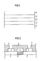
- a silicon crystal 1 of a few 100 microns thick serves as a mechanical support. Only a few lie on its surface Micrometer thick active zone 2, the electrically important structures such as transistors, capacitors, resistors and conductor tracks, eg made of aluminum or polysilicon.
- the active area is mechanically and electrically protected at the top by an electrically insulating passivation layer 3, which can consist, for example, of silicon nitride.
- the protective layer 4 according to the invention lies above this.
- the circuit is completely surrounded by a housing material 5.
- the protective layer 4 shields the underlying circuit parts in the active layer 2 from any electrical analysis as an equipotential surface. Since it is fixed to the underlying layers, removal will destroy the electrical function of the circuit. In particular, damage or destruction of the external contacts can be associated therewith (not shown).
- FIG 2, 3 and 4 show an embodiment of the invention, in which the protective layer 4, 4a is included as an active conductor in a safety logic. Removal of the protective layer 4, 4a interrupts the function of the circuit in the protected area 6 underneath.
- a corresponding arrangement can be produced by a method known as "hump technology" for the assembly of integrated circuits on substrates or film. With these bumps e.g. Chips are soldered directly onto the base.
- the protective layer 4 which in this example consists of copper and further metal layers, is now applied with the steps of the formation of the bumps, is isolated by the bump technology and structured according to the desired arrangement of the underlying circuits to be protected.
- the photo technique required for the production of bumps for etching the contact windows in the passivation layer can also be used.
- FIG. 2 shows a cross section through a circuit structured according to the invention
- FIG. 3 schematically shows a surface of a circuit. With Kl, K2, K3, K4, plated-through holes through the passivation layer are designated.
- the lines SP1, SP2 now represent, by way of example, the inner column lines of a memory field to be protected against unauthorized reading with two readout amplifiers V1, V2.
- V1, V2 the readout amplifiers
- two transistors T1, T2 located in the column lines SP1, SP2 are connected via one Control signal LES blocked. If this is not the case, both column lines are fixed to log. Zero.
- the protective layer according to the invention is integrated in the transmission of this control signal LES to the transistors T1, T2, the protective layer 4 lying between the plated-through holes K4 and K3 covering the memory field to be protected.
- the additional protective layer 4a lying as a conductor path between the plated-through holes K1 and K2, to which the inverted control signal LES is applied, is an additional protective measure against attempts to selectively remove the protective layer 4 in an unauthorized manner, for example by etching.
- Each interruption of the protective layers 4, 4a leads to a switching through of the two transistors T1 and T2 because of a logic gate 8 (NAND gate), to which the two connections are fed.
- NAND gate logic gate 8
- the plated-through holes K1, K2 and K3 are geometrically so close together that, for example, contacting with measuring tips after an etching test is made more difficult.
- the transistors T1, T2 are also conductive because of the logic gate connected downstream.
Abstract
Description
- Die Erfindung betrifft eine monolithisch integrierte Halbleiterschaltung, wie sie im Oberbegriff des Anspruchs 1 beschrieben ist.
- Bekanntlich werden MOS-Schaltungen in mehreren Verfahrensschritten hergestellt, in welchen das verwendete Halbleitersubstrat auf die gewünschte Weise strukturiert wird. Umgekehrt kann durch Analyse der Struktur die Funktion und Eigenschaft der Schaltung ermittelt werden. Mit Hilfe eines Lichtmikroskops ist es möglich, eine lichtoptische Analyse durchzuführen. Auf diese Weise kann beispielsweise auch die in einem ROM gespeicherte Information bekannt werden. Bei elektrisch programmierbaren Speichern (E PROMs) kann der Speicherinhalt einer elektrischen Analyse unterzogen werden, beispielsweise durch Abtastung des Ladungszustandes der Speicherzellen mit Elektronenstrahlen und Untersuchung des Potentialkontrastes. Eine indirekte Analyse durch Rückwirkung des Speicherzustandes auf die notwendigerweise mit dem Speicher verschaltete Peripherielogik ist ebenfalls nicht auszuschließen. Ein Beispiel dafür ist die Messung des Potentials auf den Spaltenleitungen nach Einstellung einer Speicheradresse. Derartige Messungen setzen allerdings voraus, daß die Oberfläche vollständig offenliegt und elektrooptisch abgetastet werden kann.
- Es gibt jedoch Anwendungsfälle für integrierte Schaltungen, insbesondere für Speicherschaltungen, in welchen eine Analyse der Schaltung und des Speicherinhalts für Unberechtigte verhindert werden muß. Anwendungsbeispiele dafür sind Sicherheits- und Zugriffssysteme, Abrechnungs- und Registriersysteme und Debit- oder Kreditsysteme, bei welchem sog. Chipkarten eingesetzt werden. Auf jeder Karte sind dabei Daten gespeichert, die vor jeder Anwendung der Karte geprüft werden und die einen Mißbrauch der Karte verhindern sollen. Ferner kann jeder Chip mit einer speziellen Sicherheitslogik versehen sein, welche die Auslöseschaltung des Speichers sperren oder aber das Auslesen von einer Freigabeprozedur abhängig machen soll. Die Möglichkeit einer Analyse der Schaltung oder des Speicherinhalts in betrügerischer Absicht kann daher die Zuverlässigkeit des betreffenden Systems gefährden.
- Der Erfindung lag daher die Aufgabe zugrunde, eine integrierte Schaltung der o.g. Art anzugeben, mit welcher eine elektrische Analyse der Schaltung und des Schaltungszustandes verhindert wird.
- Diese Aufgabe wird mit den Merkmalen gelöst, die im kennzeichnenden Teil des Anspruchs 1 beschrieben sind. Weitere Ausgestaltungen der Erfindung ergeben sich aus den Unteransprüchen.
- Im folgenden wird die Erfindung anhand eines Ausführungsbeispieles weiter beschrieben.
-
- Fig. 1 und Fig. 2 zeigen jeweils eine Schnittzeichnung durch eine schematisierte integrierte Schaltung,
- Fig. 3, 4 zeigen ein Anwendungsbeispiel.
- In Fig. 1 ist der Aufbau einer integrierten MOS-Schaltung in Silikon-Gate-Technik wiedergegeben. Ein Siliciumkristall 1 von einigen 100 µm Dicke dient als mechanischer Träger. Auf seiner Oberfläche liegen in einigen nur wenigen Mikrometer dicken aktiven Zone 2, die elektrisch wichtigen Strukturen wie Transistoren, Kapazitäten, Widerstände und Leiterbahnen, z.B. aus Aluminium oder Polysilicium. Nach oben ist der aktive Bereich mechanisch und elektrisch durch eine elektrisch isolierende Passivierungsschicht 3 geschützt, die beispielsweise aus Siliciumnitrid bestehen kann. Darüber liegt die erfindungsgemäße Schutzschicht 4. Schließlich wird die Schaltung vollständig von einem Gehäusematerial 5 umgeben. Die Schutzschicht 4 schirmt als Equipotentialfläche die darunterliegenden Schaltungsteile in der aktiven Schicht 2 gegen jegliche elektrische Analyse ab. Da sie fest mit den darunterliegenden Schichten verbunden ist, hat eine Entfernung eine Zerstörung der elektrischen Funktion der Schaltung zu Folge. Insbesondere kann damit eine Beschädigung oder Zerstörung der äußeren Kontakte verbunden sein (nicht dargestellt).
- Fig. 2, 3 und 4 zeigen eine Ausführungsform der Erfindung, bei welcher die Schutzschicht 4, 4a als aktive Leiterbahn in eine Sicherheitslogik mit einbezogen ist. Eine Beseitigung der Schutzschicht 4, 4a unterbricht die Funktion der Schaltung in dem darunterliegenden geschützten Bereich 6.
- Eine entsprechende Anordnung ist durch ein Verfahren herstellbar, das als "Höckertechnik" für die Montage von integrierten Schaltkreisen auf Substraten oder Film bekannt ist. Mit diesen Höckern werden z.B. Chips direkt auf die Unterlage gelötet. Mit den Arbeitsgängen der Höckerstellung wird nun auch die Schutzschicht 4, die in diesem Beispiel aus Kupfer und weiteren Metallschichten besteht, aufgebracht, durch die Höckertechnik isoliert und entsprechend der gewünschten Anordnung der darunterliegenden und zu schützenden Schaltungen strukturiert. Die bei der Höckerherstellung benötigte Phototechnik zum Ätzen der Kontaktfenster in die Passivierungsschicht läßt sich ebenfalls anwenden.
- Während Fig. 2 einen Querschnitt durch eine erfindungsgemäß strukturierte Schaltung zeigt, ist in Fig. 3 schematisch eine Oberfläche einer Schaltung wiedergegeben. Mit Kl, K2, K3, K4, sind Durchkontaktierungen durch die Passivierungsschicht bezeichnet.
- Aus Fig. 4 ist beispielhaft die Einbeziehung von Schutzschichten 4, 4a in eine Schaltungsanordnung einer sogenannten Sicherheitslogik entnehmbar. Die Leitungen SP1, SP2 stellen nun beispielhaft die gegen ein unbefugten Auslesen zu schützenden, inneren Spaltenleitungen eines Speicherfeldes mit zwei Ausleseverstärkern Vl, V2 dar. Bei einem berechtigten Zugriff auf das Speicherfeld werden zwei in den Spaltenleitungen SP1, SP2 liegenden Transistoren Tl, T2 über ein Steuersignal LES gesperrt. Ist dies nicht der Fall, so liegen beide Spaltenleitungen fest auf log. Null.
- Die erfindungsgemäße Schutzschicht ist in die Übertragung dieses Steuersignals LES an die Transistoren Tl, T2 eingebunden, wobei die zwischen den Durchkontaktierungen K4 und K3 liegende Schutzschicht 4 das zu schützende Speicherfeld abdeckt. Die als Leiterbahn zwischen den Durchkontaktierungen Kl und K2 liegende weitere Schutzschicht 4a, welche mit dem invertierten Steuersignal LES beaufschlagt ist, ist eine zusätzliche Schutzmaßnahme gegen Versuche die Schutzschicht 4 selektiv in unberechtigter Weise zu entfernen, beispielsweise durch Abätzen. Jede Unterbrechung der Schutzschichten 4, 4a führt wegen eines logischen Gatters 8 (NAND-Gatter), welchem die beiden Verbindungen zugeführt sind, zu einem Durchschalten der beiden Transistoren Tl und T2.
- Wie Fig. 3 zeigt, liegen die Durchkontaktierungen Kl, K2 und K3 geometrisch so dicht zusammen, daß beispielsweise eine Kontaktierung mit Meßspitzen nach einem Ätzversuch erschwert wird. Sobald die beiden Schutzschichten 4, 4a elektrische Berührung aufweisen, sind ebenfalls wegen des nachgeschalteten logischen Gatters die Transistoren Tl, T2 leitend.
Claims (5)
Priority Applications (1)
| Application Number | Priority Date | Filing Date | Title |
|---|---|---|---|
| AT84115850T ATE47505T1 (de) | 1984-07-31 | 1984-12-19 | Monolithisch integrierte halbleiterschaltung. |
Applications Claiming Priority (2)
| Application Number | Priority Date | Filing Date | Title |
|---|---|---|---|
| DE3428235 | 1984-07-31 | ||
| DE3428235 | 1984-07-31 |
Publications (2)
| Publication Number | Publication Date |
|---|---|
| EP0169941A1 true EP0169941A1 (de) | 1986-02-05 |
| EP0169941B1 EP0169941B1 (de) | 1989-10-18 |
Family
ID=6242034
Family Applications (1)
| Application Number | Title | Priority Date | Filing Date |
|---|---|---|---|
| EP84115850A Expired EP0169941B1 (de) | 1984-07-31 | 1984-12-19 | Monolithisch integrierte Halbleiterschaltung |
Country Status (5)
| Country | Link |
|---|---|
| US (1) | US4814849A (de) |
| EP (1) | EP0169941B1 (de) |
| JP (1) | JPS6142920A (de) |
| AT (1) | ATE47505T1 (de) |
| DE (1) | DE3480247D1 (de) |
Cited By (16)
| Publication number | Priority date | Publication date | Assignee | Title |
|---|---|---|---|---|
| FR2608317A1 (fr) * | 1986-12-15 | 1988-06-17 | Dassault Electronique | Circuit integre protege par une resine |
| EP0298848A2 (de) * | 1987-07-10 | 1989-01-11 | STMicroelectronics S.A. | Elektronischer Detektor für einen binären logischen Pegel |
| FR2617979A1 (fr) * | 1987-07-10 | 1989-01-13 | Thomson Semiconducteurs | Dispositif de detection de la depassivation d'un circuit integre |
| GB2223355A (en) * | 1988-10-01 | 1990-04-04 | Plessey Co Plc | Protective coating |
| EP0378306A2 (de) * | 1989-01-12 | 1990-07-18 | General Instrument Corporation Of Delaware | Schützen eines integrierten Schaltungschips mit einem leitenden Schild |
| EP0458306A2 (de) * | 1990-05-24 | 1991-11-27 | Kabushiki Kaisha Toshiba | Tragbarer Informationsträger und Informationsverarbeitungsgerät |
| US5608359A (en) * | 1995-10-10 | 1997-03-04 | Motorola, Inc. | Function-differentiated temperature compensated crystal oscillator and method of producing the same |
| FR2740553A1 (fr) * | 1995-10-26 | 1997-04-30 | Sgs Thomson Microelectronics | Procede de detection de presence de passivation dans un circuit integre |
| WO1997047040A1 (en) * | 1996-05-30 | 1997-12-11 | Shellcase Ltd. | I.c. device with concealed conductor lines |
| WO1998008257A1 (de) * | 1996-08-20 | 1998-02-26 | Siemens Aktiengesellschaft | Integrierte schaltung |
| US5821582A (en) * | 1993-07-22 | 1998-10-13 | National Semiconductor Corp. | Structures for preventing reverse engineering of integrated circuits |
| FR2772967A1 (fr) * | 1997-12-18 | 1999-06-25 | Sgs Thomson Microelectronics | Cellule de memoire eeprom protegee |
| WO2000011719A1 (de) * | 1998-08-18 | 2000-03-02 | Infineon Technologies Ag | Halbleiterchip mit oberflächenabdeckung |
| EP1067604A2 (de) * | 1999-07-09 | 2001-01-10 | Oki Electric Industry Company, Limited | Halbleiteranordnung mit eigener Sicherheitsfunktion |
| DE10109220A1 (de) * | 2001-02-26 | 2002-09-12 | Infineon Technologies Ag | Integrierte Schaltung mit einer Stützkapazität |
| DE102008036422A1 (de) * | 2008-08-05 | 2010-02-11 | Infineon Technologies Ag | Halbleiter-Chip mit Prüfeinrichtung |
Families Citing this family (9)
| Publication number | Priority date | Publication date | Assignee | Title |
|---|---|---|---|---|
| JP2778060B2 (ja) * | 1988-11-21 | 1998-07-23 | 日本電気株式会社 | 半導体集積回路装置 |
| EP0387383B1 (de) * | 1989-03-17 | 1995-05-24 | Siemens Aktiengesellschaft | Autarkes photonengetriebenes Bauelement |
| US5442225A (en) * | 1993-08-13 | 1995-08-15 | Lsi Logic Corporation | Integrated circuit having interconnects with ringing suppressing elements |
| USD402964S (en) * | 1996-04-08 | 1998-12-22 | Lightolier Divsion of the Genlyte Group Incorporated | Lighting fixture track system |
| US6483304B1 (en) | 1997-03-13 | 2002-11-19 | Ricoh Company, Ltd. | Magnetic field probe having a shielding and isolating layers to protect lead wires extending between a coil and pads |
| JP2001188891A (ja) * | 2000-01-05 | 2001-07-10 | Shinko Electric Ind Co Ltd | 非接触型icカード |
| DE10111027C1 (de) * | 2001-03-07 | 2002-08-08 | Infineon Technologies Ag | Schaltung für FIB-Sensor |
| US6459629B1 (en) * | 2001-05-03 | 2002-10-01 | Hrl Laboratories, Llc | Memory with a bit line block and/or a word line block for preventing reverse engineering |
| US8201746B2 (en) * | 2006-01-24 | 2012-06-19 | Agency For Science, Technology And Research | On-chip antenna and a method of fabricating the same |
Citations (4)
| Publication number | Priority date | Publication date | Assignee | Title |
|---|---|---|---|---|
| GB1251456A (de) * | 1969-06-12 | 1971-10-27 | ||
| FR2471051A1 (fr) * | 1979-11-30 | 1981-06-12 | Dassault Electronique | Circuit integre a transistors mos protege contre l'analyse et carte comprenant un tel circuit |
| WO1982004161A1 (en) * | 1981-05-21 | 1982-11-25 | Ishihara Shokichi | Device for preventing a computer program from being copied |
| EP0085117A1 (de) * | 1982-01-28 | 1983-08-10 | Mannesmann Kienzle GmbH | Schaltungsanordnung zur Sicherung von Daten in volatilen Schreib-Lese-Speichern (RAM) |
Family Cites Families (1)
| Publication number | Priority date | Publication date | Assignee | Title |
|---|---|---|---|---|
| US3518494A (en) * | 1964-06-29 | 1970-06-30 | Signetics Corp | Radiation resistant semiconductor device and method |
-
1984
- 1984-12-19 AT AT84115850T patent/ATE47505T1/de not_active IP Right Cessation
- 1984-12-19 DE DE8484115850T patent/DE3480247D1/de not_active Expired
- 1984-12-19 EP EP84115850A patent/EP0169941B1/de not_active Expired
-
1985
- 1985-07-26 JP JP60165631A patent/JPS6142920A/ja active Pending
-
1987
- 1987-10-27 US US07/117,348 patent/US4814849A/en not_active Expired - Lifetime
Patent Citations (4)
| Publication number | Priority date | Publication date | Assignee | Title |
|---|---|---|---|---|
| GB1251456A (de) * | 1969-06-12 | 1971-10-27 | ||
| FR2471051A1 (fr) * | 1979-11-30 | 1981-06-12 | Dassault Electronique | Circuit integre a transistors mos protege contre l'analyse et carte comprenant un tel circuit |
| WO1982004161A1 (en) * | 1981-05-21 | 1982-11-25 | Ishihara Shokichi | Device for preventing a computer program from being copied |
| EP0085117A1 (de) * | 1982-01-28 | 1983-08-10 | Mannesmann Kienzle GmbH | Schaltungsanordnung zur Sicherung von Daten in volatilen Schreib-Lese-Speichern (RAM) |
Cited By (34)
| Publication number | Priority date | Publication date | Assignee | Title |
|---|---|---|---|---|
| FR2608317A1 (fr) * | 1986-12-15 | 1988-06-17 | Dassault Electronique | Circuit integre protege par une resine |
| EP0298848A2 (de) * | 1987-07-10 | 1989-01-11 | STMicroelectronics S.A. | Elektronischer Detektor für einen binären logischen Pegel |
| FR2617979A1 (fr) * | 1987-07-10 | 1989-01-13 | Thomson Semiconducteurs | Dispositif de detection de la depassivation d'un circuit integre |
| EP0300864A2 (de) * | 1987-07-10 | 1989-01-25 | STMicroelectronics S.A. | Anordnung zur Detektion der Ablösung der Passivierungsschicht einer integrierten Schaltung |
| EP0300864A3 (en) * | 1987-07-10 | 1989-03-01 | Sgs-Thomson Microelectronics S.A. | Apparatus for the detection of integrated-circuit de-passivation |
| US4868489A (en) * | 1987-07-10 | 1989-09-19 | Sgs-Thomson Microelectronics, S.A. | Device to detect the depassivation of an integrated circuit |
| EP0298848A3 (en) * | 1987-07-10 | 1990-02-14 | Sgs-Thomson Microelectronics S.A. | Electronic detector for a logic binary level |
| GB2223355A (en) * | 1988-10-01 | 1990-04-04 | Plessey Co Plc | Protective coating |
| EP0378306A2 (de) * | 1989-01-12 | 1990-07-18 | General Instrument Corporation Of Delaware | Schützen eines integrierten Schaltungschips mit einem leitenden Schild |
| EP0378306A3 (de) * | 1989-01-12 | 1991-12-04 | General Instrument Corporation Of Delaware | Schützen eines integrierten Schaltungschips mit einem leitenden Schild |
| EP0920057A3 (de) * | 1989-01-12 | 2000-01-12 | General Instrument Corporation | Schützen eines integrierten Schaltungschips mit einem leitenden Schild |
| EP0920057A2 (de) * | 1989-01-12 | 1999-06-02 | General Instrument Corporation | Schützen eines integrierten Schaltungschips mit einem leitenden Schild |
| EP0458306A2 (de) * | 1990-05-24 | 1991-11-27 | Kabushiki Kaisha Toshiba | Tragbarer Informationsträger und Informationsverarbeitungsgerät |
| EP0458306A3 (en) * | 1990-05-24 | 1992-12-02 | Kabushiki Kaisha Toshiba | Portable medium and information processing apparatus |
| US5821582A (en) * | 1993-07-22 | 1998-10-13 | National Semiconductor Corp. | Structures for preventing reverse engineering of integrated circuits |
| US5608359A (en) * | 1995-10-10 | 1997-03-04 | Motorola, Inc. | Function-differentiated temperature compensated crystal oscillator and method of producing the same |
| FR2740553A1 (fr) * | 1995-10-26 | 1997-04-30 | Sgs Thomson Microelectronics | Procede de detection de presence de passivation dans un circuit integre |
| EP0771030A1 (de) * | 1995-10-26 | 1997-05-02 | STMicroelectronics S.A. | Passivierungs-Detektionsverfahren für integrierte Schaltungen |
| WO1997047040A1 (en) * | 1996-05-30 | 1997-12-11 | Shellcase Ltd. | I.c. device with concealed conductor lines |
| WO1998008257A1 (de) * | 1996-08-20 | 1998-02-26 | Siemens Aktiengesellschaft | Integrierte schaltung |
| DE19633549C2 (de) * | 1996-08-20 | 2002-07-11 | Infineon Technologies Ag | Integrierte Schaltung mit einer sich zumindest teilweise über einen Sägekanal hinweg erstreckenden Schutzschicht |
| EP0926737A3 (de) * | 1997-12-18 | 1999-07-14 | STMicroelectronics S.r.l. | Eine geschützte EEPROM Zelle |
| FR2772967A1 (fr) * | 1997-12-18 | 1999-06-25 | Sgs Thomson Microelectronics | Cellule de memoire eeprom protegee |
| US6151245A (en) * | 1997-12-18 | 2000-11-21 | Stmicroelectronics, S.R.L. | Screened EEPROM cell |
| EP0926737A2 (de) * | 1997-12-18 | 1999-06-30 | STMicroelectronics S.r.l. | Eine geschützte EEPROM Zelle |
| WO2000011719A1 (de) * | 1998-08-18 | 2000-03-02 | Infineon Technologies Ag | Halbleiterchip mit oberflächenabdeckung |
| US6452283B2 (en) | 1998-08-18 | 2002-09-17 | Infineon Technologies Ag | Semiconductor chip with surface cover |
| US6359338B1 (en) | 1999-07-09 | 2002-03-19 | Oki Electric Industry Co., Ltd. | Semiconductor apparatus with self-security function |
| EP1067604A3 (de) * | 1999-07-09 | 2002-03-27 | Oki Electric Industry Company, Limited | Halbleiteranordnung mit eigener Sicherheitsfunktion |
| EP1067604A2 (de) * | 1999-07-09 | 2001-01-10 | Oki Electric Industry Company, Limited | Halbleiteranordnung mit eigener Sicherheitsfunktion |
| EP1610382A2 (de) * | 1999-07-09 | 2005-12-28 | Oki Electric Industry Company, Limited | Halbleiteranordnung mit eigener Sicherheitsfunktion |
| EP1610382A3 (de) * | 1999-07-09 | 2008-05-28 | Oki Electric Industry Company, Limited | Halbleiteranordnung mit eigener Sicherheitsfunktion |
| DE10109220A1 (de) * | 2001-02-26 | 2002-09-12 | Infineon Technologies Ag | Integrierte Schaltung mit einer Stützkapazität |
| DE102008036422A1 (de) * | 2008-08-05 | 2010-02-11 | Infineon Technologies Ag | Halbleiter-Chip mit Prüfeinrichtung |
Also Published As
| Publication number | Publication date |
|---|---|
| US4814849A (en) | 1989-03-21 |
| DE3480247D1 (en) | 1989-11-23 |
| EP0169941B1 (de) | 1989-10-18 |
| JPS6142920A (ja) | 1986-03-01 |
| ATE47505T1 (de) | 1989-11-15 |
Similar Documents
| Publication | Publication Date | Title |
|---|---|---|
| EP0169941B1 (de) | Monolithisch integrierte Halbleiterschaltung | |
| DE69922722T2 (de) | Oberflächenform-Erkennungssensor und dessen Herstellungsverfahren | |
| DE102005047414B4 (de) | Magnetoresistives Sensormodul und Verfahren zum Herstellen desselben | |
| DE3727142C2 (de) | Verfahren zur Herstellung von Mikrosensoren mit integrierter Signalverarbeitung | |
| EP0178512B1 (de) | MOS-Schaltung mit einem E2-PROM | |
| DE102006010777A1 (de) | Überprüfungsvorrichtung für einen Feuchtigkeitssensor und Verfahren zum Einstellen von Sensorcharakteristiken eines Feuchtigkeitssensors | |
| DE102005047482A1 (de) | Magnetoresistives Sensormodul und Verfahren zum Herstellen desselben | |
| DE102016102291B4 (de) | Halbleiterchip mit bruchdetektion | |
| DE19814857C2 (de) | Gassensor nach dem Prinzip der Austrittsarbeitsmessung | |
| WO2000041241A1 (de) | Vertikal integrierte halbleiteranordnung | |
| DE102018220169A1 (de) | Verfahren zum herstellen eines feuchtigkeitssensors auf waferebene und feuchtigkeitssensor | |
| DE102004058411B3 (de) | Halbleiterwafer mit einer Teststruktur und Verfahren | |
| WO2000011719A1 (de) | Halbleiterchip mit oberflächenabdeckung | |
| EP0221351A1 (de) | Integrierte Halbleiterschaltung mit einem elektrisch leitenden Flächenelement | |
| EP1103808B1 (de) | Gassensor | |
| EP1016140B1 (de) | Verdrahtungsverfahren für halbleiter-bauelemente zur verhinderung von produktpiraterie und produktmanipulation, durch das verfahren hergestelltes halbleiter-bauelement und verwendung des halbleiter-bauelements in einer chipkarte | |
| DE19743264A1 (de) | Verfahren zur Herstellung einer Emulationsschaltkreisanordnung sowie Anordnung mit zwei integrierten Schaltkreisen | |
| EP0427328B1 (de) | Verfahren zum Herstellen von integrierten Schaltungen sowie integrierte Schaltung | |
| DE19749539A1 (de) | Halbleiterbaustein | |
| DE10213609A1 (de) | Elektrisches Bauelement mit einem Kontakt und Verfahren zum Ausbilden eines Kontaktes auf einem Halbleitermaterial | |
| DE3327503A1 (de) | Teststruktur zur kennzeichnung von halbleiterchips und verfahren zu deren kennzeichnung | |
| DE19748666C2 (de) | Verdrahtungsverfahren für mikroelektronische Systeme zur Verhinderung von Produktpiraterie und Produktmanipulation, durch das Verfahren hergestelltes mikroelektronisches System und Verwendung des mikroelektronischen Systems in einer Chipkarte | |
| DE102004010299B4 (de) | Infrarot-Empfänger-Chip | |
| DE10140045A1 (de) | IC-Chip mit Schutzstruktur | |
| DE19746642C2 (de) | Verfahren zur Herstellung eines Halbleiterbauelements sowie dessen Verwendung in einer Chipkarte |
Legal Events
| Date | Code | Title | Description |
|---|---|---|---|
| PUAI | Public reference made under article 153(3) epc to a published international application that has entered the european phase |
Free format text: ORIGINAL CODE: 0009012 |
|
| 17P | Request for examination filed |
Effective date: 19841219 |
|
| AK | Designated contracting states |
Designated state(s): AT CH DE FR GB IT LI NL SE |
|
| 17Q | First examination report despatched |
Effective date: 19880104 |
|
| GRAA | (expected) grant |
Free format text: ORIGINAL CODE: 0009210 |
|
| AK | Designated contracting states |
Kind code of ref document: B1 Designated state(s): AT CH DE FR GB IT LI NL SE |
|
| REF | Corresponds to: |
Ref document number: 47505 Country of ref document: AT Date of ref document: 19891115 Kind code of ref document: T |
|
| REF | Corresponds to: |
Ref document number: 3480247 Country of ref document: DE Date of ref document: 19891123 |
|
| ET | Fr: translation filed | ||
| ITF | It: translation for a ep patent filed |
Owner name: STUDIO JAUMANN |
|
| GBT | Gb: translation of ep patent filed (gb section 77(6)(a)/1977) | ||
| PLBE | No opposition filed within time limit |
Free format text: ORIGINAL CODE: 0009261 |
|
| STAA | Information on the status of an ep patent application or granted ep patent |
Free format text: STATUS: NO OPPOSITION FILED WITHIN TIME LIMIT |
|
| 26N | No opposition filed | ||
| ITTA | It: last paid annual fee | ||
| PGFP | Annual fee paid to national office [announced via postgrant information from national office to epo] |
Ref country code: NL Payment date: 19901231 Year of fee payment: 7 |
|
| PG25 | Lapsed in a contracting state [announced via postgrant information from national office to epo] |
Ref country code: NL Effective date: 19920701 |
|
| NLV4 | Nl: lapsed or anulled due to non-payment of the annual fee | ||
| EAL | Se: european patent in force in sweden |
Ref document number: 84115850.4 |
|
| REG | Reference to a national code |
Ref country code: GB Ref legal event code: IF02 |
|
| PGFP | Annual fee paid to national office [announced via postgrant information from national office to epo] |
Ref country code: GB Payment date: 20031126 Year of fee payment: 20 |
|
| PGFP | Annual fee paid to national office [announced via postgrant information from national office to epo] |
Ref country code: CH Payment date: 20031201 Year of fee payment: 20 Ref country code: AT Payment date: 20031201 Year of fee payment: 20 |
|
| PGFP | Annual fee paid to national office [announced via postgrant information from national office to epo] |
Ref country code: SE Payment date: 20031202 Year of fee payment: 20 |
|
| PGFP | Annual fee paid to national office [announced via postgrant information from national office to epo] |
Ref country code: FR Payment date: 20031209 Year of fee payment: 20 |
|
| PGFP | Annual fee paid to national office [announced via postgrant information from national office to epo] |
Ref country code: DE Payment date: 20040218 Year of fee payment: 20 |
|
| PG25 | Lapsed in a contracting state [announced via postgrant information from national office to epo] |
Ref country code: LI Free format text: LAPSE BECAUSE OF EXPIRATION OF PROTECTION Effective date: 20041218 Ref country code: GB Free format text: LAPSE BECAUSE OF EXPIRATION OF PROTECTION Effective date: 20041218 Ref country code: CH Free format text: LAPSE BECAUSE OF EXPIRATION OF PROTECTION Effective date: 20041218 |
|
| REG | Reference to a national code |
Ref country code: GB Ref legal event code: PE20 |
|
| REG | Reference to a national code |
Ref country code: CH Ref legal event code: PL |
|
| EUG | Se: european patent has lapsed | ||
| EUG | Se: european patent has lapsed |