EP0178512B1 - MOS-Schaltung mit einem E2-PROM - Google Patents
MOS-Schaltung mit einem E2-PROM Download PDFInfo
- Publication number
- EP0178512B1 EP0178512B1 EP85112212A EP85112212A EP0178512B1 EP 0178512 B1 EP0178512 B1 EP 0178512B1 EP 85112212 A EP85112212 A EP 85112212A EP 85112212 A EP85112212 A EP 85112212A EP 0178512 B1 EP0178512 B1 EP 0178512B1
- Authority
- EP
- European Patent Office
- Prior art keywords
- mos circuit
- memory
- circuit according
- sensors
- blocking
- Prior art date
- Legal status (The legal status is an assumption and is not a legal conclusion. Google has not performed a legal analysis and makes no representation as to the accuracy of the status listed.)
- Expired
Links
Images

Classifications
-
- G—PHYSICS
- G07—CHECKING-DEVICES
- G07F—COIN-FREED OR LIKE APPARATUS
- G07F7/00—Mechanisms actuated by objects other than coins to free or to actuate vending, hiring, coin or paper currency dispensing or refunding apparatus
- G07F7/08—Mechanisms actuated by objects other than coins to free or to actuate vending, hiring, coin or paper currency dispensing or refunding apparatus by coded identity card or credit card or other personal identification means
- G07F7/10—Mechanisms actuated by objects other than coins to free or to actuate vending, hiring, coin or paper currency dispensing or refunding apparatus by coded identity card or credit card or other personal identification means together with a coded signal, e.g. in the form of personal identification information, like personal identification number [PIN] or biometric data
- G07F7/1008—Active credit-cards provided with means to personalise their use, e.g. with PIN-introduction/comparison system
-
- G—PHYSICS
- G06—COMPUTING; CALCULATING OR COUNTING
- G06K—GRAPHICAL DATA READING; PRESENTATION OF DATA; RECORD CARRIERS; HANDLING RECORD CARRIERS
- G06K19/00—Record carriers for use with machines and with at least a part designed to carry digital markings
- G06K19/06—Record carriers for use with machines and with at least a part designed to carry digital markings characterised by the kind of the digital marking, e.g. shape, nature, code
- G06K19/067—Record carriers with conductive marks, printed circuits or semiconductor circuit elements, e.g. credit or identity cards also with resonating or responding marks without active components
- G06K19/07—Record carriers with conductive marks, printed circuits or semiconductor circuit elements, e.g. credit or identity cards also with resonating or responding marks without active components with integrated circuit chips
- G06K19/073—Special arrangements for circuits, e.g. for protecting identification code in memory
- G06K19/07309—Means for preventing undesired reading or writing from or onto record carriers
- G06K19/07372—Means for preventing undesired reading or writing from or onto record carriers by detecting tampering with the circuit
-
- G—PHYSICS
- G06—COMPUTING; CALCULATING OR COUNTING
- G06Q—INFORMATION AND COMMUNICATION TECHNOLOGY [ICT] SPECIALLY ADAPTED FOR ADMINISTRATIVE, COMMERCIAL, FINANCIAL, MANAGERIAL OR SUPERVISORY PURPOSES; SYSTEMS OR METHODS SPECIALLY ADAPTED FOR ADMINISTRATIVE, COMMERCIAL, FINANCIAL, MANAGERIAL OR SUPERVISORY PURPOSES, NOT OTHERWISE PROVIDED FOR
- G06Q20/00—Payment architectures, schemes or protocols
- G06Q20/30—Payment architectures, schemes or protocols characterised by the use of specific devices or networks
- G06Q20/34—Payment architectures, schemes or protocols characterised by the use of specific devices or networks using cards, e.g. integrated circuit [IC] cards or magnetic cards
- G06Q20/341—Active cards, i.e. cards including their own processing means, e.g. including an IC or chip
-
- G—PHYSICS
- G07—CHECKING-DEVICES
- G07F—COIN-FREED OR LIKE APPARATUS
- G07F7/00—Mechanisms actuated by objects other than coins to free or to actuate vending, hiring, coin or paper currency dispensing or refunding apparatus
- G07F7/08—Mechanisms actuated by objects other than coins to free or to actuate vending, hiring, coin or paper currency dispensing or refunding apparatus by coded identity card or credit card or other personal identification means
- G07F7/0806—Details of the card
- G07F7/0813—Specific details related to card security
- G07F7/082—Features insuring the integrity of the data on or in the card
-
- G—PHYSICS
- G11—INFORMATION STORAGE
- G11C—STATIC STORES
- G11C16/00—Erasable programmable read-only memories
- G11C16/02—Erasable programmable read-only memories electrically programmable
- G11C16/06—Auxiliary circuits, e.g. for writing into memory
- G11C16/22—Safety or protection circuits preventing unauthorised or accidental access to memory cells
-
- G—PHYSICS
- G11—INFORMATION STORAGE
- G11C—STATIC STORES
- G11C5/00—Details of stores covered by group G11C11/00
- G11C5/005—Circuit means for protection against loss of information of semiconductor storage devices
-
- H—ELECTRICITY
- H01—ELECTRIC ELEMENTS
- H01L—SEMICONDUCTOR DEVICES NOT COVERED BY CLASS H10
- H01L23/00—Details of semiconductor or other solid state devices
- H01L23/57—Protection from inspection, reverse engineering or tampering
- H01L23/576—Protection from inspection, reverse engineering or tampering using active circuits
-
- H—ELECTRICITY
- H01—ELECTRIC ELEMENTS
- H01L—SEMICONDUCTOR DEVICES NOT COVERED BY CLASS H10
- H01L2924/00—Indexing scheme for arrangements or methods for connecting or disconnecting semiconductor or solid-state bodies as covered by H01L24/00
- H01L2924/0001—Technical content checked by a classifier
- H01L2924/0002—Not covered by any one of groups H01L24/00, H01L24/00 and H01L2224/00
Definitions
- the invention relates to a monolithically integrated MOS circuit with a memory field made of electrically programmable memory cells (E 2 PROM).
- E 2 PROM electrically programmable memory cells
- the memory content can be subjected to an analysis by means of an electro-optical potential probe method by scanning the state of charge of the memory cells with electron or X-rays and examining the potential contrast, from which direct or indirect conclusions can be drawn about the programming state.
- the invention was therefore based on the object of an integrated circuit of the above. Specify the type whose memory is protected from electro-optical analysis.
- the invention is based on the fact that when radiation is used, at least some of the memory cells are switched on the output side to a defined potential regardless of the state of charge of the memory cells and the stored information is therefore not recognizable.
- This is achieved in that one or more radiation-sensitive sensors are integrated in the vicinity of the memory cells, the output signal of which is preferably used for the defined definition of those applied to the memory outputs. Column tension is used. When exposed to radiation, the sensors change their output signal and influence the level of the column lines. The column line potential becomes independent of the state of charge of the memory cells. The memory content is therefore not changed.
- the invention also has the advantage that sensors designed as pn diodes can be integrated into the generally used n-channel double silicon silicon gate technology using standard manufacturing steps.
- FIG. 1 shows a memory array 1 a with a multiplicity of memory cells 5 arranged in a matrix, each of which consists of a selection transistor 6 and a memory transistor 7 of the floating gate type connected in series. All selection transistors 6 of a row can be controlled via a selection line 3 and all memory transistors 7 via a programming line 4.
- the memory cells 5 are read out column by column via a column line 2 which is connected to a first operating voltage Upp via a load transistor 18.
- the memory array 1 a is also equipped with radiation-sensitive sensors (8), which in the example shown consist of two photodiodes 8.
- Blocking circuits 10a are located between the diodes 8 and at least one column line 2. When activated by the sensors, they suppress every readout on the associated column line 2.
- the diodes 8 In the regular operating state, ie without the storage field 1a being exposed to radiation, the diodes 8 are blocked by a second operating voltage Ucc of a few volts and are weakly conductive. The output voltages of the diodes 8 rise to log because of a load transistor 11 of the self-conducting or normally-off type. 1. When exposed to light or radiation, 8 pairs of charge carriers are generated along a pn limit of the diodes, which cause a diode current and log the output voltages of the sensors. Zero.
- each diode 8 is inverted to the control gate of at least one further normally-off transistor 12 which is connected to a column line 2.
- these transistors 12 receive a positive control voltage and become conductive. You switch the column potentials to log. Zero as long as the radiation continues.
- One or more of the further transistors 12 are assigned to each column line 2. If a plurality of diodes 8 or further transistors 12 are arranged in the memory array 1, the output signals of all the diodes 8 are inverted via NAND gates 13 and clamped together the other transistors 12 laid.
- the inverters advantageously also have an amplifier and / or a Schmitt trigger function.
- the senor is implemented by a photoresistor 14 and the blocking circuit 10b by a transistor 16 controlled by a self-conducting transistor 15.
- the control input of transistor 16 is pulled to ground and blocked by self-conducting transistor 15.
- the control input of transistor 16 is connected to an operating voltage U cc via photoresistor 14 and switched to conductive, column line 2 being pulled to ground by its controlled path.
- the photoresistor 14 can also be designed as a polysilicon sheet resistor using standard technology
- Photothyristors are also suitable as sensors.
- sensors photodiodes 8, photoresistor 14
- associated blocking circuits are provided and connected independently of one another, as the example in FIG. 1 shows.
- the sensors are arranged geometrically distributed within the memory field 1a, 1b.
- Several sensors act via a log. Linking, in the example according to FIG. 1, via the two NAND gates 13 to the blocking circuit 10a, 10b or column line 2.
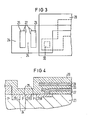
- a diode 8 and the associated load transistor 11 is shown in FIGS. 3 and 4.
- the manufacture of a pn diode can be integrated into the commonly used n-channel double silicon silicon gate technology using standard manufacturing steps.
- such a diode advantageously has a finger or stripe structure with an increased length of the pn limit 22.
- n + -doped zones 24 are produced on a p-substrate 23 with a first mask by means of a conventional source-drain doping.
- the p-regions 25 of the photodiode are protected against the source-drain assignment and retain the doping type of the base material.
- the p-regions 25 of the cathode of the photodiode have a ground potential applied to them via the substrate 23.
- a silicon oxide layer 26 is removed above the p-regions 25 of the diode.
- the arrangement is closed over the entire surface with a silicon nitride layer 29.
- the leads of the load transistor 11 and all leads relating to the blocking circuit 10a, b are connected and connected via a silicon layer 27 and so-called burried contacts 30. They are shielded from the outside by a further poly-silicon layer 20 lying above.
Description
- Die Erfindung betrifft eine monolithisch integrierte MOS-Schaltung mit einem Speicherfeld aus elektrisch programmierbaren Speicherzellen (E2PROM).
- Aus der Zeitschrift "Electronics", 28. Feb. 1980, Seite 113 bis 117, ist eine Speicheranordnung mit elektrisch programmierbaren Speicherzellen bekannt, die jeweils ein Steuer- und ein Speichergate (Floating-Gate) aufweisen. Durch Anlegen einer positiven oder negativen Programmierspannung wird dabei eine auf einem Tunneleffekt beruhende Elektronenverschiebung aus bzw. in das Speichergate bewirkt.
- Der Speicherinhalt kann mit Hilfe eines elektrooptischen Potential-Sondenverfahrens durch Abtasten des Ladungszustands der Speicherzellen mit Elektronen- oder Röntgenstrahlen und Untersuchung des Potentialkontrastes einer Analyse unterzogen werden, aus welcher direkt oder indirekt Schlüsse auf den Programmierzustand zu ziehen sind.
- Es gibt jedoch Anwendungsfälle für Speicherschaltungen, bei welchen eine Offenbarung des Speicherinhalts für Unberechtigte verhindert werden muß. Anwendungsbeispiele dafür sind Sicherheits-und Zugriffssysteme, Abrechnungs- und Registriersysteme und Debit- oder Kreditsysteme, bei welchen sog. Chipkarten eingesetzt werden. Auf jeder dieser Karten sind dabei individuelle Daten gespeichert, die vor jeder Anwendung der Karte geprüft werden, und die einen Mißbrauch der Karte verhindern sollen. Die Möglichkeit einer Analyse des Speicherinhalts in betrügerischer Absicht kann daher die Zuverlässigkeit des betreffenden Systems gefährden.
- Der Erfindung lag daher die Aufgabe zugrunde, eine integrierte Schaltung der o.g. Art anzugeben, deren Speicher vor einer elektrooptischen Analyse geschützt ist.
- Diese Aufgabe wird gemäß dem kennzeichnenden Teil des Anspruchs 1 gelöst.
- Die Erfindung beruht darauf, daß beim Einsatz von Strahlung zumindest ein Teil der Speicherzellen ausgangsseitig auf ein definiertes Potential unabhängig vom Ladungszustand der Speicherzellen geschaltet wird und damit die gespeicherte Information nicht erkennbar ist. Dies wird, dadurch erreicht, daß im Umfeld der Speicherzellen ein- oder mehrere strahlungsempfindliche Sensoren integriert sind, deren Ausgangssignal vorzugsweise zur definierten Festlegung der an den Speicherausgängen anliegenden . Spaltenspannung benützt wird. Bei Bestrahlung ändern die Sensoren ihr Ausgangssignal und nehmen Einfluß auf den Pegel der Spaltenleitungen. Das Spaltenleitungspotential wird dabei unabhängig vom Ladungszustand der Speicherzellen. Der Speicherinhalt wird also nicht verändert.
- Die Erfindung hat ferner den Vorteil, daß als pn-Dioden ausgebildete Sensoren mit Hilfe standardmäßiger Fertigungsschritte in die allgemein verwendeten n-Kanal-Doppelsilizium-Silicon-Gate-Technik eingebunden werden können.
- Weiterbildungen der Erfindung ergeben sich aus den Unteransprüchen.
- Im folgenden wird die Erfindung anhand zweier Ausführungsbeispiele weiter beschrieben.
- Fig. 1, 2 zeigen jeweils eine erfindungsgemäße Speicherzelle.
- Fig 3 zeigt eine Aufsicht auf eine Speicherzelle.
- Fig. 4 zeigt einen Querschnitt durch die Speicherzelle gemäß Fig. 3.
- Fig. 1 zeigt ein Speicherfeld 1a mit einer Vielzahl von matrixförmig angeordneten Speicherzellen 5, die jeweils aus einem Auswahltransistor 6 und einem in Reihe geschalteten Speichertransistor 7 vom Floating-Gate-Typ bestehen. Alle Auswahltransistoren 6 einer Zeile sind über eine Auswahlleitung 3 und alle Speichertransistoren 7 über eine Programmierleitung 4 ansteuerbar. Die Speicherzellen 5 werden spaltenweise über eine Spaltenleitung 2 ausgelesen, die über einen Lasttransistor 18 an einer ersten Betriebsspannung Upp liegt.
- Das Speicherfeld 1a ist ferner mit strahlungsempfindlichen Sensoren (8) bestückt, die im Wiedergegebenen Beispiel aus zwei Photodioden 8 bestehen. Zwischen den Dioden 8 und mindestens einer Spaltenleitung 2 liegen Sperrschaltungen 10a. Bei Ansteuerung durch die Sensoren unterdrücken sie jeden Auslesevorgang auf der zugehörigen Spaltenleitung 2.
- Im regulären Betriebszustand, d.h. ohne daß das Speicherfeld 1a einer Strahlung ausgesetzt ist, sind die Dioden 8 durch eine zweite Betriebsspannung Ucc von einigen Volt gesperrt und schwach leitend. Die Ausgangsspannungen der Dioden 8 riegen dabei wegen eines Lasttransistors 11 vom selbstleitenden oder selbstsperrenden Typ auf log. 1. Bei Licht- oder Strahlungseinwirkung werden entlang einer pn-Grenze der Dioden 8 Ladungsträgerpaare erzeugt, die einen Diodenstrom bewirken und die Ausgangsspannungen der Sensoren auf log. Null legen.
- Das Ausgangssignal einer jeden Diode 8 wird invertiert an das Steuergate mindestens eines weiteren selbstsperrenden Transistors 12 geführt, der mit einer Spaltenleitung 2 verbunden ist. Bei Strahlungseinfall erhalten diese Transistoren 12 eine positive Steuerspannung und werden leitend. Sie schalten die Spaltenpotentiale auf log. Null, solange die Strahlung anhält. Jeder Spaltenleitung 2 sind ein oder mehrere der weiteren Transistoren 12 zugeordnet. Sind mehrere Dioden 8 bzw. weitere Transistoren 12 im Speicherfeld 1 angeordnet, so werden die Ausgangssignale aller Dioden 8 über NAND-Gatter 13 invertiert und zusammengeklammert an die weiteren Transistoren 12 gelegt. Die Inverter besitzen vorteilhafterweise auch eine Verstärker-und/oder eine Schmitt-Trigger-Funktion.
- In dem Ausführungsbeispiel der Fig. 2 mit einem Speicherfeld 1 b ist der Sensor durch einen Photowiderstand 14 und die Sperrschaltung 10b durch einen von einem selbstleitenden Transistor 15 angesteuerten Transistor 16 realisiert. Solange der Photowiderstand 14 keiner Bestrahlung ausgesetzt ist, ist er schwachleitend. In diesem Zustand wird der Steuereingang des Transistors 16 durch den selbstleitenden Transistor 15 auf Masse gezogen und gesperrt. Bei einer harten Einstrahlung und Photoleitung wird der Steuereingang des Transistor 16 über den Photowiderstand 14 mit einer Betriebsspannung Ucc verbunden und leitend geschaltet, wobei die Spaltenleitung 2 durch seine gesteuerte Strecke auf Masse gezogen wird. Der Photowiderstand 14 läßt sich mit Standardtechnik auch als Polysilicium-Bahnwiderstand ausführen
- Als Sensoren sind beispielsweise auch Photothyristoren geeignet.
- Um bereits bei einer Teilbestrahlung des Speicherfeldes 1a, 1b eine Sperrung der Auslesevorgänge zu erreichen, sind - wie das Beispiel der Fig. 1 zeigt - mehrere Sensoren (Photodioden 8, Photowiderstand 14) und zugehörige Sperrschaltungen vorgesehen und unabhängig voneinander verschaltet. Die Sensoren sind innerhalb des Speicherfeldes 1a, 1b geometrisch verteilt angeordnet. Mehrere Sensoren wirken dabei über eine log. Verknüpfung, im Beispiel gemäß Fig. 1 über die beiden NAND-Gatter 13 auf die Sperrschaltung 10a, 10b bzw. Spaltenleitung 2.
- Aus den Figuren 3 und 4 ist der Aufbau einer Diode 8 und des zugehörigen Lasttransistors 11 wiedergegeben. Die Herstellung einer pn-Diode kann mit Hilfe standardmäßiger Fertigungsschritte in die allgemein verwendete n-Kanal-Doppelsilizium-Silicon-Gate-Technik eingebunden werden. Zur Erhöhung der Strahlungsempfindlichkeit weist eine derartige Diode vorteilhafterweise eine Finger- bzw. Streifenstruktur mit erhöhter Länge der pn-Grenze 22 auf. Gemäß dem Beispiel werden auf ein p-Substrat 23 mit einer ersten Maske n + -dotierte Zonen 24 mittels einer üblichen Source-Drain-Dotierung erzeugt. Die p-Bereiche 25 der Photodiode sind gegen die Source-Drain-Belegung geschützt und behalten den Dotierungstyp des Grundmaterials.
- Die p-Gebiete 25 der Kathode der Photodiode sind über das Substrat 23 mit einem Massepotential beaufschlagt. Oberhalb der p-Bereiche 25 der Diode ist eine Siliciumoxidschicht 26 entfernt. Die Anordnung wird nach außen ganzflächig mit einer Siliciumnitridschicht 29 abgeschlossen. Ferner werden die Zuleitungen des Lasttransistors 11 und alle die Sperrschaltung 10a, b betreffenden Zuleitungen über eine Silicium-Schicht 27 und sog. Burried-Kontakte 30 angeschlossen und verbunden. Sie werden von einer weiteren, darüber liegenden Poly-Silicium-Schicht 20 nach außen abgeschirmt.
Claims (6)
Priority Applications (1)
| Application Number | Priority Date | Filing Date | Title |
|---|---|---|---|
| AT85112212T ATE43744T1 (de) | 1984-09-27 | 1985-09-26 | Mos-schaltung mit einem e2-prom. |
Applications Claiming Priority (2)
| Application Number | Priority Date | Filing Date | Title |
|---|---|---|---|
| DE3435495 | 1984-09-27 | ||
| DE3435495 | 1984-09-27 |
Publications (2)
| Publication Number | Publication Date |
|---|---|
| EP0178512A1 EP0178512A1 (de) | 1986-04-23 |
| EP0178512B1 true EP0178512B1 (de) | 1989-05-31 |
Family
ID=6246514
Family Applications (1)
| Application Number | Title | Priority Date | Filing Date |
|---|---|---|---|
| EP85112212A Expired EP0178512B1 (de) | 1984-09-27 | 1985-09-26 | MOS-Schaltung mit einem E2-PROM |
Country Status (5)
| Country | Link |
|---|---|
| US (1) | US4910707A (de) |
| EP (1) | EP0178512B1 (de) |
| JP (1) | JPS6184054A (de) |
| AT (1) | ATE43744T1 (de) |
| DE (1) | DE3570792D1 (de) |
Families Citing this family (21)
| Publication number | Priority date | Publication date | Assignee | Title |
|---|---|---|---|---|
| US5107139A (en) * | 1990-03-30 | 1992-04-21 | Texas Instruments Incorporated | On-chip transient event detector |
| US5053992A (en) * | 1990-10-04 | 1991-10-01 | General Instrument Corporation | Prevention of inspection of secret data stored in encapsulated integrated circuit chip |
| DE4212111C2 (de) * | 1992-04-10 | 2003-05-22 | Angewandte Digital Elektronik | Indikation unsachgemäß behandelter Chipkarten |
| JPH0793977A (ja) * | 1993-04-26 | 1995-04-07 | Samsung Electron Co Ltd | 半導体メモリ装置の中間電圧発生回路 |
| GB2319602B (en) * | 1996-11-21 | 2000-10-04 | Motorola Ltd | Light detection device |
| EP1128248B1 (de) * | 2000-02-21 | 2016-09-14 | Infineon Technologies AG | Halbleiterchip mit einem lichtempfindlichen Element |
| DE10101995A1 (de) * | 2001-01-18 | 2002-07-25 | Philips Corp Intellectual Pty | Schaltungsanordnung und Verfahren zum Schützen mindestens einer Chipanordnung vor Manipulation und/oder vor Mißbrauch |
| US6459629B1 (en) * | 2001-05-03 | 2002-10-01 | Hrl Laboratories, Llc | Memory with a bit line block and/or a word line block for preventing reverse engineering |
| DE10140045B4 (de) * | 2001-08-16 | 2006-05-04 | Infineon Technologies Ag | IC-Chip mit Schutzstruktur |
| DE10206186B4 (de) * | 2002-02-14 | 2010-01-28 | Infineon Technologies Ag | Speichermatrix und Verfahren zur Absicherung einer Speichermatrix |
| DE10218096A1 (de) * | 2002-04-23 | 2003-11-13 | Infineon Technologies Ag | Integrierte Schaltung |
| DE10221790A1 (de) * | 2002-05-15 | 2003-11-27 | Giesecke & Devrient Gmbh | Verfahren zur Sicherung des Speicherinhalts von IC-Karten |
| DE10345240A1 (de) * | 2003-09-29 | 2005-05-04 | Infineon Technologies Ag | Integrierte Schaltung mit Strahlungssensoranordnung |
| US8997255B2 (en) * | 2006-07-31 | 2015-03-31 | Inside Secure | Verifying data integrity in a data storage device |
| US8352752B2 (en) * | 2006-09-01 | 2013-01-08 | Inside Secure | Detecting radiation-based attacks |
| US20080061843A1 (en) * | 2006-09-11 | 2008-03-13 | Asier Goikoetxea Yanci | Detecting voltage glitches |
| US8410583B2 (en) * | 2007-09-04 | 2013-04-02 | Nds Limited | Security chip |
| GB2488583A (en) * | 2011-03-03 | 2012-09-05 | Nds Ltd | Preventing unauthorized access to data stored in non-volatile memories |
| WO2017138773A1 (ko) * | 2016-02-12 | 2017-08-17 | 한양대학교 산학협력단 | 보안 반도체 칩 및 그 동작 방법 |
| US10778679B2 (en) * | 2016-02-12 | 2020-09-15 | Industry-University Cooperation Foundation Hanyang University | Secure semiconductor chip and operating method thereof |
| US11316210B2 (en) | 2018-11-21 | 2022-04-26 | Samsung Sdi Co., Ltd. | Control unit for a battery module or system |
Family Cites Families (10)
| Publication number | Priority date | Publication date | Assignee | Title |
|---|---|---|---|---|
| US3551761A (en) * | 1968-08-13 | 1970-12-29 | Ibm | Integrated photodiode array |
| US3696250A (en) * | 1970-09-17 | 1972-10-03 | Rca Corp | Signal transfer system for panel type image sensor |
| US3721963A (en) * | 1972-03-13 | 1973-03-20 | North American Rockwell | Photon to digital converter using photon flux integration |
| US4499557A (en) * | 1980-10-28 | 1985-02-12 | Energy Conversion Devices, Inc. | Programmable cell for use in programmable electronic arrays |
| US4417325A (en) * | 1981-07-13 | 1983-11-22 | Eliyahou Harari | Highly scaleable dynamic ram cell with self-signal amplification |
| US4677742A (en) * | 1983-01-18 | 1987-07-07 | Energy Conversion Devices, Inc. | Electronic matrix arrays and method for making the same |
| US4608672A (en) * | 1983-07-14 | 1986-08-26 | Honeywell Inc. | Semiconductor memory |
| US4714901A (en) * | 1985-10-15 | 1987-12-22 | Gould Inc. | Temperature compensated complementary metal-insulator-semiconductor oscillator |
| US4722822A (en) * | 1985-11-27 | 1988-02-02 | Advanced Micro Devices, Inc. | Column-current multiplexing driver circuit for high density proms |
| GB8531347D0 (en) * | 1985-12-19 | 1986-01-29 | Goran K | Optoelectronic dynamic memory device |
-
1985
- 1985-09-24 JP JP60210898A patent/JPS6184054A/ja active Pending
- 1985-09-26 AT AT85112212T patent/ATE43744T1/de not_active IP Right Cessation
- 1985-09-26 EP EP85112212A patent/EP0178512B1/de not_active Expired
- 1985-09-26 DE DE8585112212T patent/DE3570792D1/de not_active Expired
-
1989
- 1989-01-30 US US07/304,873 patent/US4910707A/en not_active Expired - Lifetime
Also Published As
| Publication number | Publication date |
|---|---|
| US4910707A (en) | 1990-03-20 |
| EP0178512A1 (de) | 1986-04-23 |
| JPS6184054A (ja) | 1986-04-28 |
| DE3570792D1 (en) | 1989-07-06 |
| ATE43744T1 (de) | 1989-06-15 |
Similar Documents
| Publication | Publication Date | Title |
|---|---|---|
| EP0178512B1 (de) | MOS-Schaltung mit einem E2-PROM | |
| EP0160720B1 (de) | Halbleiterspeicherzelle mit einem potentialmässig schwebenden Speichergate | |
| DE2632036C2 (de) | Integrierte Speicherschaltung mit Feldeffekttransistoren | |
| EP0103043B1 (de) | CMOS-Speicherzelle mit potentialmässig schwebendem Speichergate | |
| EP0169941B1 (de) | Monolithisch integrierte Halbleiterschaltung | |
| DE3103160A1 (de) | Nichtfluechtiger eprom mit erhoehtem wirkungsgrad | |
| DE1524838A1 (de) | Informationsspeicher | |
| DE69830867T2 (de) | Halbleiteranordnung mit einer leitenden Schutzschicht | |
| DE102021108242A1 (de) | Bildsensor mit einer Anordung von optisch schaltbaren magnetischen Tunnelkontakten | |
| DE112004002678B4 (de) | Elektrisch programmierbares 2-Transistoren-Sicherungselement mit einfacher Polysiliziumschicht und elektrisch programmierbare Transistor-Sicherungszelle | |
| DE3115695A1 (de) | Integrierte halbleiterschaltung | |
| DE4411442C2 (de) | Nichtflüchtiger Halbleiterspeicher | |
| DE3833726C2 (de) | ||
| DE19807009A1 (de) | Verfahren zur Herstellung einer nichtflüchtigen Speichereinrichtung | |
| EP0719454B1 (de) | Halbleiter(detektor)struktur | |
| DE69635842T2 (de) | Speicherredundanzschaltung, die einzelne polysilizium-schwebegattertransistoren als redundanzelemente verwendet | |
| DE2904812A1 (de) | Halbleiteranordnung | |
| EP0045403B1 (de) | Verefahren zur Herstellung einer Anordnung zum Verringern der Strahlungsempfindlichkeit von in integrierter MOS-Schaltkreistechnik ausgeführten Speicherzellen | |
| DE3032306C2 (de) | ||
| EP0221351A1 (de) | Integrierte Halbleiterschaltung mit einem elektrisch leitenden Flächenelement | |
| DE112018005789T5 (de) | Esd-geschützter halbleiter-photomultiplikator | |
| WO2003017350A2 (de) | Ic-chip mit schutzstruktur | |
| DE2952159A1 (de) | Ir-bildaufnahmeeinrichtung | |
| EP1128248A1 (de) | Halbleiterchip mit einem lichtempfindlichen Element | |
| DE19510070C1 (de) | Strahlungssensoreinrichtung zum Erfassen der Häufigkeit einer auf diese auftreffenden Strahlung |
Legal Events
| Date | Code | Title | Description |
|---|---|---|---|
| PUAI | Public reference made under article 153(3) epc to a published international application that has entered the european phase |
Free format text: ORIGINAL CODE: 0009012 |
|
| AK | Designated contracting states |
Kind code of ref document: A1 Designated state(s): AT CH DE FR GB IT LI NL SE |
|
| 17P | Request for examination filed |
Effective date: 19861010 |
|
| 17Q | First examination report despatched |
Effective date: 19881114 |
|
| GRAA | (expected) grant |
Free format text: ORIGINAL CODE: 0009210 |
|
| AK | Designated contracting states |
Kind code of ref document: B1 Designated state(s): AT CH DE FR GB IT LI NL SE |
|
| REF | Corresponds to: |
Ref document number: 43744 Country of ref document: AT Date of ref document: 19890615 Kind code of ref document: T |
|
| REF | Corresponds to: |
Ref document number: 3570792 Country of ref document: DE Date of ref document: 19890706 |
|
| ET | Fr: translation filed | ||
| ITF | It: translation for a ep patent filed |
Owner name: STUDIO JAUMANN |
|
| GBT | Gb: translation of ep patent filed (gb section 77(6)(a)/1977) | ||
| PLBE | No opposition filed within time limit |
Free format text: ORIGINAL CODE: 0009261 |
|
| STAA | Information on the status of an ep patent application or granted ep patent |
Free format text: STATUS: NO OPPOSITION FILED WITHIN TIME LIMIT |
|
| 26N | No opposition filed | ||
| PGFP | Annual fee paid to national office [announced via postgrant information from national office to epo] |
Ref country code: NL Payment date: 19900930 Year of fee payment: 6 |
|
| ITTA | It: last paid annual fee | ||
| PG25 | Lapsed in a contracting state [announced via postgrant information from national office to epo] |
Ref country code: NL Effective date: 19920401 |
|
| NLV4 | Nl: lapsed or anulled due to non-payment of the annual fee | ||
| EAL | Se: european patent in force in sweden |
Ref document number: 85112212.7 |
|
| PGFP | Annual fee paid to national office [announced via postgrant information from national office to epo] |
Ref country code: AT Payment date: 20010816 Year of fee payment: 17 |
|
| PGFP | Annual fee paid to national office [announced via postgrant information from national office to epo] |
Ref country code: GB Payment date: 20010912 Year of fee payment: 17 |
|
| PGFP | Annual fee paid to national office [announced via postgrant information from national office to epo] |
Ref country code: SE Payment date: 20010913 Year of fee payment: 17 |
|
| PGFP | Annual fee paid to national office [announced via postgrant information from national office to epo] |
Ref country code: FR Payment date: 20010928 Year of fee payment: 17 |
|
| PGFP | Annual fee paid to national office [announced via postgrant information from national office to epo] |
Ref country code: DE Payment date: 20011119 Year of fee payment: 17 |
|
| PGFP | Annual fee paid to national office [announced via postgrant information from national office to epo] |
Ref country code: CH Payment date: 20011207 Year of fee payment: 17 |
|
| REG | Reference to a national code |
Ref country code: GB Ref legal event code: IF02 |
|
| PG25 | Lapsed in a contracting state [announced via postgrant information from national office to epo] |
Ref country code: GB Free format text: LAPSE BECAUSE OF NON-PAYMENT OF DUE FEES Effective date: 20020926 Ref country code: AT Free format text: LAPSE BECAUSE OF NON-PAYMENT OF DUE FEES Effective date: 20020926 |
|
| PG25 | Lapsed in a contracting state [announced via postgrant information from national office to epo] |
Ref country code: SE Free format text: LAPSE BECAUSE OF NON-PAYMENT OF DUE FEES Effective date: 20020927 |
|
| PG25 | Lapsed in a contracting state [announced via postgrant information from national office to epo] |
Ref country code: LI Free format text: LAPSE BECAUSE OF NON-PAYMENT OF DUE FEES Effective date: 20020930 Ref country code: CH Free format text: LAPSE BECAUSE OF NON-PAYMENT OF DUE FEES Effective date: 20020930 |
|
| PG25 | Lapsed in a contracting state [announced via postgrant information from national office to epo] |
Ref country code: DE Free format text: LAPSE BECAUSE OF NON-PAYMENT OF DUE FEES Effective date: 20030401 |
|
| EUG | Se: european patent has lapsed | ||
| GBPC | Gb: european patent ceased through non-payment of renewal fee |
Effective date: 20020926 |
|
| REG | Reference to a national code |
Ref country code: CH Ref legal event code: PL |
|
| PG25 | Lapsed in a contracting state [announced via postgrant information from national office to epo] |
Ref country code: FR Free format text: LAPSE BECAUSE OF NON-PAYMENT OF DUE FEES Effective date: 20030603 |
|
| REG | Reference to a national code |
Ref country code: FR Ref legal event code: ST |