EP0168121A1 - Verfahren und Vorrichtung zum Speicherzugriff in Mehrprozessorsystemen - Google Patents
Verfahren und Vorrichtung zum Speicherzugriff in Mehrprozessorsystemen Download PDFInfo
- Publication number
- EP0168121A1 EP0168121A1 EP85300858A EP85300858A EP0168121A1 EP 0168121 A1 EP0168121 A1 EP 0168121A1 EP 85300858 A EP85300858 A EP 85300858A EP 85300858 A EP85300858 A EP 85300858A EP 0168121 A1 EP0168121 A1 EP 0168121A1
- Authority
- EP
- European Patent Office
- Prior art keywords
- data
- processor
- content
- location
- memory
- Prior art date
- Legal status (The legal status is an assumption and is not a legal conclusion. Google has not performed a legal analysis and makes no representation as to the accuracy of the status listed.)
- Granted
Links
Images
Classifications
-
- G—PHYSICS
- G06—COMPUTING; CALCULATING OR COUNTING
- G06F—ELECTRIC DIGITAL DATA PROCESSING
- G06F12/00—Accessing, addressing or allocating within memory systems or architectures
- G06F12/02—Addressing or allocation; Relocation
- G06F12/08—Addressing or allocation; Relocation in hierarchically structured memory systems, e.g. virtual memory systems
- G06F12/0802—Addressing of a memory level in which the access to the desired data or data block requires associative addressing means, e.g. caches
- G06F12/0806—Multiuser, multiprocessor or multiprocessing cache systems
- G06F12/084—Multiuser, multiprocessor or multiprocessing cache systems with a shared cache
Definitions
- This invention is in the field of data processing and, in particular, relates to a method and apparatus for the resolution of memory access demands in multiple processor systems.
- processors In many advanced data processing systems, a number of independent processors can have access to a main memory shared by the system. When a processor wishes only to read a particular memory location or even rewrite a specified location, access can be controlled sequentially with little cost in performance. However, it is also common for processors to perform an operation known as a read-modify-write (RMW) operation or the like. This operation involves reading data out of a selected memory location, processing the data read out, and writing modified data back into the specified location.
- RMW read-modify-write
- the problem of handling multiple access requests can become acute when one of the independent processors is carrying out instructions on a string of data, such as moving a string of ASCII-coded data. Since the 8-bit ASCII words (representing language characters, punctuation, etc.) are smaller than the typical 16 bit (or 32 bit) registers around which advanced systems are designed, a modification which involves changing less than the full 16 (or 32) bits often is not controlled by the system hardware.
- a 32-bit wide memory register common to a number of processors can store two data blocks consisting of an integer value (i.e., a fortran * 2 integer) on one side (the upper 16 bits) and two ASCII characters on the other side (the lower 16 bits).
- an integer value i.e., a fortran * 2 integer
- ASCII characters on the other side
- the lower 16 bits the integer value
- a first processor wished to replace the ASCII characters only, it would need to read the entire register, modify the contents to keep the integer value on one side while changing the characters on the other side and then write the modified 32-bits into the memory. Since this RMW operation cannot occur instantaneously, a second processor might write a new entry into part of the register in the interim (i.e., to replace the integer value) and this data would be lost if the first processor was allowed to enter its modification without any controls.
- the solution to date has been to exclude the second processor in one fashion or another while the first processor performs a RMW operation.
- the present invention resides in an improved data processing system and method wherein a plurality of processors can concurrently operate on the system's memory even when one processor is performing a read-modify-write (RMW) operation a particular memory location.
- RMW read-modify-write
- the conventional techniques of "freezing" the memory bus or deactivating a block of data are avoided by employing a content-associative write buffer in conjunction with a memory controller which locks the associated location until the read-modify-write operation is completed.
- a buffer is used to store a series of write instructions from a processor until the memory bus is cleared.
- the buffer is a content associative buffer which also permits a processor seeking to read data to poll the buffer for latest data.
- the content- associate buffer also permits the controller to control new entries whenever data is undergoing a RMW operation.
- a field in microcode is provided for the issuance of a directive whenever a read-modify-write sequence is initiated by a processor.
- the directive i.e., "TAKE A LOCK”
- the directive is dumped into the write buffer at the appropriate address with a tag bit denoting the operation as a lock -- not a write, as well as another tag bit identifying the processor.
- processors seeking to merely read data from the same location will not be impeded and such other processors, in fact, can also write new data for insertion into the memory location.
- new data transmitted to the memory location will not be entered but rather will remain in the write buffer until the read-modify-write process of the first processor is completed.
- microcode instructions further prevent the overwriting of the second processor's data by the first processor, thereby reversing the typical process wherein a second write command to same address in write buffer overrides any data residing there.
- uninterrupted processing essentially is maintained for the two processors .
- This technique can be applied as well to the case of three or more processors by extrapolation.
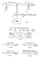
- a general block diagram of the memory access system 10 including at least two processors 12 and 14 connected to a common memory 18 via a memory bus 16 which includes a data path 16a, an address path 16b, and a command path 16c.
- a memory bus 16 which includes a data path 16a, an address path 16b, and a command path 16c.
- the common memory 18 is typically a high speed MOS memory of about one megabyte although the access system could also be implemented with different types of memories or memories of different sizes.
- controller 20 Interposed between the processors 12, 14 and the memory 18 is a controller 20 and a locking content-associative write buffer 22.
- the controller 20 is similar is most aspects to conventional controllers used to control access to memory locations.
- the controller 20 is implemented by a combination of hardware and firmware (or microcode).
- controller 20 can include microcode instructions for identifying RMW requests for addressing and formatting the buffer 20, and for issuing the necessary directives as described below to lock particular addresses, and to transfer data back and forth between the processors 12, 14, the memory 18 and the buffer 22.
- Implementation of the buffer 22 can be achieved with commercially available components or individualized designs by those skilled in the art.
- the content-associative structure is an address-organised buffer accessed by applying the address word. In one preferred embodiment, the structure contains four addressed entries.
- the structure of the buffer 22 is shown in wore detail in Fig. 2.
- the buffer includes a plurality of address blocks A, B, etc.
- Each address in buffer 22 corresponds to a memory location in the main memory 18.
- Associated with each address are two sixteen-bit strings of data Al ... A16 and A17 ... A32, a validity bit for each string VI, V2, a lock bit L, and at least one bit for identifying the processor that issues the lock directive ID. (For the case of two processors, only one bit is typically needed to distinguish between processors; however, for three or more processors, additional bits would be needed).
- Each of the two sixteen-bit strings of data stored in buffer 22 is called a "data block".
- the two data blocks make up a memory data word. In the illustrated embodiment, data is transfered as a block or set of two blocks. Sixteen-bit blocks are the minimum size for a data transmission.
- the structure described above is intended for use in a system where the data path of the memory bus can accomodate thirty-two bit wide data transmissions and the operating system is designed to assure the integrity of sixteen-bit block transmissions as well.
- the teachings herein can also be applied to sixteen-bit data transmissions and eight-bit data block designs as well.
- Figs. 3a through 3d The operation of the memory access scheme is shown schematically in Figs. 3a through 3d.
- a single entry in buffer 22 is shown in its initial state containing data from any one of the processors connected to the system.
- controller 20 sets the lock bit (i.e., to a "1" value) and the validity bits VI and V2 are initialized as well (i.e., to a " 0 " value) indicating that one of the first or second data blocks is being modified.
- the processor performing the modification is also identified at the same time by the identification bit IL (i.e., set to " ⁇ " for CPU ).
- the controller recognizes the address sought as a locked address and takes the necessary steps to preserve this new data while the RMW operation is being completed. For example, if as shown in Fig. 3c, were to write new data for the first data block, the validity bit V1 associated with that block would be set (i.e., to a "I" value) indicating that this new data is to be saved at the expense of any modified data subsequently written by CPU e. (It is assumed that proper programming prevents the second processor from seeking to change that portion of the data in the buffer that is being modified by the first processor). When the first processor completes its modification of data as shown in Fig.
Priority Applications (1)
| Application Number | Priority Date | Filing Date | Title |
|---|---|---|---|
| AT85300858T ATE64020T1 (de) | 1984-02-10 | 1985-02-08 | Verfahren und vorrichtung zum speicherzugriff in mehrprozessorsystemen. |
Applications Claiming Priority (2)
| Application Number | Priority Date | Filing Date | Title |
|---|---|---|---|
| US578797 | 1984-02-10 | ||
| US06/578,797 US4561051A (en) | 1984-02-10 | 1984-02-10 | Memory access method and apparatus in multiple processor systems |
Publications (2)
| Publication Number | Publication Date |
|---|---|
| EP0168121A1 true EP0168121A1 (de) | 1986-01-15 |
| EP0168121B1 EP0168121B1 (de) | 1991-05-29 |
Family
ID=24314358
Family Applications (1)
| Application Number | Title | Priority Date | Filing Date |
|---|---|---|---|
| EP85300858A Expired - Lifetime EP0168121B1 (de) | 1984-02-10 | 1985-02-08 | Verfahren und Vorrichtung zum Speicherzugriff in Mehrprozessorsystemen |
Country Status (6)
| Country | Link |
|---|---|
| US (1) | US4561051A (de) |
| EP (1) | EP0168121B1 (de) |
| JP (1) | JPS60237567A (de) |
| AT (1) | ATE64020T1 (de) |
| CA (1) | CA1223973A (de) |
| DE (1) | DE3582962D1 (de) |
Cited By (2)
| Publication number | Priority date | Publication date | Assignee | Title |
|---|---|---|---|---|
| WO1991003785A1 (en) * | 1989-09-11 | 1991-03-21 | Wang Laboratories, Inc. | Apparatus and method for maintaining cache/main memory consistency |
| GB2379531A (en) * | 2001-06-14 | 2003-03-12 | Pace Micro Tech Plc | Method for changing memory addresses so that data can be processed in an uninterrupted manner |
Families Citing this family (44)
| Publication number | Priority date | Publication date | Assignee | Title |
|---|---|---|---|---|
| JPH0760422B2 (ja) * | 1983-12-30 | 1995-06-28 | 株式会社日立製作所 | 記憶ロツク方式 |
| US4862350A (en) * | 1984-08-03 | 1989-08-29 | International Business Machines Corp. | Architecture for a distributive microprocessing system |
| US4679148A (en) * | 1985-05-01 | 1987-07-07 | Ball Corporation | Glass machine controller |
| JPS6297036A (ja) * | 1985-07-31 | 1987-05-06 | テキサス インスツルメンツ インコ−ポレイテツド | 計算機システム |
| US5291581A (en) * | 1987-07-01 | 1994-03-01 | Digital Equipment Corporation | Apparatus and method for synchronization of access to main memory signal groups in a multiprocessor data processing system |
| AU614044B2 (en) * | 1988-03-25 | 1991-08-15 | Nec Corporation | Information processing system capable of quickly detecting an extended buffer memory regardless of a state of a main memory device |
| US5301278A (en) * | 1988-04-29 | 1994-04-05 | International Business Machines Corporation | Flexible dynamic memory controller |
| US5247649A (en) * | 1988-05-06 | 1993-09-21 | Hitachi, Ltd. | Multi-processor system having a multi-port cache memory |
| US5089952A (en) * | 1988-10-07 | 1992-02-18 | International Business Machines Corporation | Method for allowing weak searchers to access pointer-connected data structures without locking |
| US5129072A (en) * | 1989-03-08 | 1992-07-07 | Hewlett-Packard Company | System for minimizing initiator processor interrupts by protocol controller in a computer bus system |
| US5179679A (en) * | 1989-04-07 | 1993-01-12 | Shoemaker Kenneth D | Apparatus and method for permitting reading of data from an external memory when data is stored in a write buffer in the event of a cache read miss |
| US5136714A (en) * | 1989-12-04 | 1992-08-04 | International Business Machines Corporation | Method and apparatus for implementing inter-processor interrupts using shared memory storage in a multi-processor computer system |
| US5131085A (en) * | 1989-12-04 | 1992-07-14 | International Business Machines Corporation | High performance shared main storage interface |
| JP2665813B2 (ja) * | 1990-02-23 | 1997-10-22 | 三菱電機株式会社 | 記憶制御装置 |
| US5446865A (en) * | 1990-03-13 | 1995-08-29 | At&T Corp. | Processor adapted for sharing memory with more than one type of processor |
| US5193167A (en) * | 1990-06-29 | 1993-03-09 | Digital Equipment Corporation | Ensuring data integrity by locked-load and conditional-store operations in a multiprocessor system |
| US5404482A (en) * | 1990-06-29 | 1995-04-04 | Digital Equipment Corporation | Processor and method for preventing access to a locked memory block by recording a lock in a content addressable memory with outstanding cache fills |
| US5276835A (en) * | 1990-12-14 | 1994-01-04 | International Business Machines Corporation | Non-blocking serialization for caching data in a shared cache |
| JP2586219B2 (ja) * | 1990-12-20 | 1997-02-26 | 日本電気株式会社 | 高速媒体優先解放型排他方式 |
| US5539911A (en) | 1991-07-08 | 1996-07-23 | Seiko Epson Corporation | High-performance, superscalar-based computer system with out-of-order instruction execution |
| US5493687A (en) | 1991-07-08 | 1996-02-20 | Seiko Epson Corporation | RISC microprocessor architecture implementing multiple typed register sets |
| US5430860A (en) * | 1991-09-17 | 1995-07-04 | International Business Machines Inc. | Mechanism for efficiently releasing memory lock, after allowing completion of current atomic sequence |
| US5506980A (en) * | 1991-10-22 | 1996-04-09 | Hitachi, Ltd. | Method and apparatus for parallel processing of a large data array utilizing a shared auxiliary memory |
| JPH05210640A (ja) * | 1992-01-31 | 1993-08-20 | Hitachi Ltd | マルチプロセッサシステム |
| WO1993020505A2 (en) | 1992-03-31 | 1993-10-14 | Seiko Epson Corporation | Superscalar risc instruction scheduling |
| JP3637920B2 (ja) | 1992-05-01 | 2005-04-13 | セイコーエプソン株式会社 | スーパースケーラマイクロプロセサに於て命令をリタイアさせるシステム及び方法 |
| DE69330889T2 (de) | 1992-12-31 | 2002-03-28 | Seiko Epson Corp | System und Verfahren zur Änderung der Namen von Registern |
| US5628021A (en) | 1992-12-31 | 1997-05-06 | Seiko Epson Corporation | System and method for assigning tags to control instruction processing in a superscalar processor |
| US5666515A (en) * | 1993-02-18 | 1997-09-09 | Unisys Corporation | Information processing system having multiple modules and a memory on a bus, where any module can lock an addressable portion of the memory by sending retry signals to other modules that try to read at the locked address |
| US5592641A (en) * | 1993-06-30 | 1997-01-07 | Intel Corporation | Method and device for selectively locking write access to blocks in a memory array using write protect inputs and block enabled status |
| US5566317A (en) * | 1994-06-14 | 1996-10-15 | International Business Machines Corporation | Method and apparatus for computer disk drive management |
| US5924128A (en) * | 1996-06-20 | 1999-07-13 | International Business Machines Corporation | Pseudo zero cycle address generator and fast memory access |
| US6055608A (en) * | 1997-04-14 | 2000-04-25 | International Business Machines Corporation | Method and system for speculatively sourcing cache memory data within a multiprocessor data-processing system |
| US6078991A (en) * | 1997-04-14 | 2000-06-20 | International Business Machines Corporation | Method and system for speculatively requesting system data bus for sourcing cache memory data within a multiprocessor data-processing system |
| US5895484A (en) * | 1997-04-14 | 1999-04-20 | International Business Machines Corporation | Method and system for speculatively accessing cache memory data within a multiprocessor data-processing system using a cache controller |
| US5924118A (en) * | 1997-04-14 | 1999-07-13 | International Business Machines Corporation | Method and system for speculatively sourcing cache memory data prior to upstream cache invalidation within a multiprocessor data-processing system |
| US6314493B1 (en) | 1998-02-03 | 2001-11-06 | International Business Machines Corporation | Branch history cache |
| US6701429B1 (en) | 1998-12-03 | 2004-03-02 | Telefonaktiebolaget Lm Ericsson(Publ) | System and method of start-up in efficient way for multi-processor systems based on returned identification information read from pre-determined memory location |
| US6567094B1 (en) * | 1999-09-27 | 2003-05-20 | Xerox Corporation | System for controlling read and write streams in a circular FIFO buffer |
| US8219762B1 (en) | 2004-08-13 | 2012-07-10 | Oracle America, Inc. | Computer system and method for leasing memory location to allow predictable access to memory location |
| US7412572B1 (en) | 2004-03-17 | 2008-08-12 | Sun Microsystems, Inc. | Multiple-location read, single-location write operations using transient blocking synchronization support |
| US7418543B2 (en) * | 2004-12-21 | 2008-08-26 | Intel Corporation | Processor having content addressable memory with command ordering |
| GB0523293D0 (en) * | 2005-11-16 | 2005-12-21 | Ibm | Apparatus and method for controlling data copy services |
| JP4973730B2 (ja) * | 2007-06-20 | 2012-07-11 | 富士通株式会社 | 演算処理装置及び演算処理装置の制御方法 |
Citations (5)
| Publication number | Priority date | Publication date | Assignee | Title |
|---|---|---|---|---|
| US3848234A (en) * | 1973-04-04 | 1974-11-12 | Sperry Rand Corp | Multi-processor system with multiple cache memories |
| US3984818A (en) * | 1974-02-09 | 1976-10-05 | U.S. Philips Corporation | Paging in hierarchical memory systems |
| US4157586A (en) * | 1977-05-05 | 1979-06-05 | International Business Machines Corporation | Technique for performing partial stores in store-thru memory configuration |
| WO1981002210A1 (en) * | 1980-01-28 | 1981-08-06 | Digital Equipment Corp | Cached multiprocessor system with pipeline timing |
| US4394733A (en) * | 1980-11-14 | 1983-07-19 | Sperry Corporation | Cache/disk subsystem |
Family Cites Families (23)
| Publication number | Priority date | Publication date | Assignee | Title |
|---|---|---|---|---|
| US3108257A (en) * | 1958-12-30 | 1963-10-22 | Ibm | Locking and unlocking of memory devices |
| US3568157A (en) * | 1963-12-31 | 1971-03-02 | Bell Telephone Labor Inc | Program controlled data processing system |
| US3435418A (en) * | 1965-05-27 | 1969-03-25 | Ibm | Record retrieval and record hold system |
| US3469239A (en) * | 1965-12-02 | 1969-09-23 | Hughes Aircraft Co | Interlocking means for a multi-processor system |
| US3508205A (en) * | 1967-01-17 | 1970-04-21 | Computer Usage Co Inc | Communications security system |
| US3573736A (en) * | 1968-01-15 | 1971-04-06 | Ibm | Interruption and interlock arrangement |
| US3528061A (en) * | 1968-07-05 | 1970-09-08 | Ibm | Interlock arrangement |
| US3551892A (en) * | 1969-01-15 | 1970-12-29 | Ibm | Interaction in a multi-processing system utilizing central timers |
| US3631405A (en) * | 1969-11-12 | 1971-12-28 | Honeywell Inc | Sharing of microprograms between processors |
| DE2064383C3 (de) * | 1970-01-12 | 1981-02-26 | Fujitsu Ltd., Kawasaki, Kanagawa (Japan) | Datenverarbeitungsanlage mit mehreren zentralen Verarbeitungseinrichtungen |
| US3725872A (en) * | 1971-03-03 | 1973-04-03 | Burroughs Corp | Data processing system having status indicating and storage means |
| US3761883A (en) * | 1972-01-20 | 1973-09-25 | Ibm | Storage protect key array for a multiprocessing system |
| GB1410631A (en) * | 1972-01-26 | 1975-10-22 | Plessey Co Ltd | Data processing system interrupt arrangements |
| US4073005A (en) * | 1974-01-21 | 1978-02-07 | Control Data Corporation | Multi-processor computer system |
| GB1536853A (en) * | 1975-05-01 | 1978-12-20 | Plessey Co Ltd | Data processing read and hold facility |
| US4000485A (en) * | 1975-06-30 | 1976-12-28 | Honeywell Information Systems, Inc. | Data processing system providing locked operation of shared resources |
| US4162529A (en) * | 1975-12-04 | 1979-07-24 | Tokyo Shibaura Electric Co., Ltd. | Interruption control system in a multiprocessing system |
| US4037215A (en) * | 1976-04-30 | 1977-07-19 | International Business Machines Corporation | Key controlled address relocation translation system |
| US4038645A (en) * | 1976-04-30 | 1977-07-26 | International Business Machines Corporation | Non-translatable storage protection control system |
| US4099243A (en) * | 1977-01-18 | 1978-07-04 | Honeywell Information Systems Inc. | Memory block protection apparatus |
| US4136386A (en) * | 1977-10-06 | 1979-01-23 | International Business Machines Corporation | Backing store access coordination in a multi-processor system |
| JPS596415B2 (ja) * | 1977-10-28 | 1984-02-10 | 株式会社日立製作所 | 多重情報処理システム |
| US4245306A (en) * | 1978-12-21 | 1981-01-13 | Burroughs Corporation | Selection of addressed processor in a multi-processor network |
-
1984
- 1984-02-10 US US06/578,797 patent/US4561051A/en not_active Expired - Fee Related
-
1985
- 1985-02-08 AT AT85300858T patent/ATE64020T1/de not_active IP Right Cessation
- 1985-02-08 JP JP60022121A patent/JPS60237567A/ja active Pending
- 1985-02-08 CA CA000473958A patent/CA1223973A/en not_active Expired
- 1985-02-08 EP EP85300858A patent/EP0168121B1/de not_active Expired - Lifetime
- 1985-02-08 DE DE8585300858T patent/DE3582962D1/de not_active Expired - Fee Related
Patent Citations (5)
| Publication number | Priority date | Publication date | Assignee | Title |
|---|---|---|---|---|
| US3848234A (en) * | 1973-04-04 | 1974-11-12 | Sperry Rand Corp | Multi-processor system with multiple cache memories |
| US3984818A (en) * | 1974-02-09 | 1976-10-05 | U.S. Philips Corporation | Paging in hierarchical memory systems |
| US4157586A (en) * | 1977-05-05 | 1979-06-05 | International Business Machines Corporation | Technique for performing partial stores in store-thru memory configuration |
| WO1981002210A1 (en) * | 1980-01-28 | 1981-08-06 | Digital Equipment Corp | Cached multiprocessor system with pipeline timing |
| US4394733A (en) * | 1980-11-14 | 1983-07-19 | Sperry Corporation | Cache/disk subsystem |
Non-Patent Citations (3)
| Title |
|---|
| IBM TECHNICAL DISCLOSURE BULLETIN, vol. 16, no. 3, August 1973, pages 926-927, New York, US; R.E. NIELSEN: "Encoded exclusive data for multiprocessing system" * |
| IBM TECHNICAL DISCLOSURE BULLETIN, vol. 19, no. 2, July 1976, pages 594-596, New York, US; J.D. JONES et al.: "Updating cache data array's with data stored by other CPU's" * |
| IBM TECHNICAL DISCLOSURE BULLETIN, vol. 23, no. 12, May 1981, pages 5329-5331, New York, US; E.G. DRIMAK et al.: "Multiprocessor locking with a bypass for channel references" * |
Cited By (4)
| Publication number | Priority date | Publication date | Assignee | Title |
|---|---|---|---|---|
| WO1991003785A1 (en) * | 1989-09-11 | 1991-03-21 | Wang Laboratories, Inc. | Apparatus and method for maintaining cache/main memory consistency |
| US5276849A (en) * | 1989-09-11 | 1994-01-04 | Wang Laboratories, Inc. | Apparatus and method for maintaining cache/main memory consistency utilizing a dual port FIFO buffer |
| GB2379531A (en) * | 2001-06-14 | 2003-03-12 | Pace Micro Tech Plc | Method for changing memory addresses so that data can be processed in an uninterrupted manner |
| GB2379531B (en) * | 2001-06-14 | 2005-05-25 | Pace Micro Tech Plc | Central processing unit architectures |
Also Published As
| Publication number | Publication date |
|---|---|
| ATE64020T1 (de) | 1991-06-15 |
| DE3582962D1 (de) | 1991-07-04 |
| JPS60237567A (ja) | 1985-11-26 |
| CA1223973A (en) | 1987-07-07 |
| EP0168121B1 (de) | 1991-05-29 |
| US4561051A (en) | 1985-12-24 |
Similar Documents
| Publication | Publication Date | Title |
|---|---|---|
| US4561051A (en) | Memory access method and apparatus in multiple processor systems | |
| US5133058A (en) | Page-tagging translation look-aside buffer for a computer memory system | |
| KR100382395B1 (ko) | 컴퓨터메모리에정보를기억하는방법및장치 | |
| US5689679A (en) | Memory system and method for selective multi-level caching using a cache level code | |
| US4471429A (en) | Apparatus for cache clearing | |
| US5247649A (en) | Multi-processor system having a multi-port cache memory | |
| US4654790A (en) | Translation of virtual and real addresses to system addresses | |
| US4481573A (en) | Shared virtual address translation unit for a multiprocessor system | |
| US6779102B2 (en) | Data processor capable of executing an instruction that makes a cache memory ineffective | |
| CA2022529C (en) | Apparatus for page tagging in a computer system | |
| US5119484A (en) | Selections between alternate control word and current instruction generated control word for alu in respond to alu output and current instruction | |
| US5034885A (en) | Cache memory device with fast data-write capacity | |
| US5313602A (en) | Multiprocessor system and method of control over order of transfer of data between buffer storages | |
| US5717916A (en) | Method for providing an improved fully associative cache memory having a finite state machine and linked list structure | |
| US4992977A (en) | Cache memory device constituting a memory device used in a computer | |
| EP0533427B1 (de) | Rechnerspeichersteuerungsanordnung | |
| US4942521A (en) | Microprocessor with a cache memory in which validity flags for first and second data areas are simultaneously readable | |
| US5737568A (en) | Method and apparatus to control cache memory in multiprocessor system utilizing a shared memory | |
| US4424564A (en) | Data processing system providing dual storage of reference bits | |
| US5737753A (en) | Least recently used block replacement for four block cache logic system | |
| US5349672A (en) | Data processor having logical address memories and purge capabilities | |
| JPS5847784B2 (ja) | キ−記憶システム | |
| JP3219810B2 (ja) | データ処理装置 | |
| JP2588547B2 (ja) | マルチcpuシステム | |
| EP0302926B1 (de) | Schaltung zur steuersignalerzeugung für eine arithmetische logische einheit in einem digitalverarbeitungsgerät |
Legal Events
| Date | Code | Title | Description |
|---|---|---|---|
| PUAI | Public reference made under article 153(3) epc to a published international application that has entered the european phase |
Free format text: ORIGINAL CODE: 0009012 |
|
| AK | Designated contracting states |
Designated state(s): AT BE CH DE FR GB IT LI LU NL SE |
|
| 17P | Request for examination filed |
Effective date: 19860623 |
|
| 17Q | First examination report despatched |
Effective date: 19880725 |
|
| GRAA | (expected) grant |
Free format text: ORIGINAL CODE: 0009210 |
|
| ITF | It: translation for a ep patent filed |
Owner name: UFFICIO BREVETTI GUAZZO |
|
| AK | Designated contracting states |
Kind code of ref document: B1 Designated state(s): AT BE CH DE FR GB IT LI LU NL SE |
|
| PG25 | Lapsed in a contracting state [announced via postgrant information from national office to epo] |
Ref country code: SE Effective date: 19910529 Ref country code: NL Effective date: 19910529 Ref country code: LI Effective date: 19910529 Ref country code: CH Effective date: 19910529 Ref country code: BE Effective date: 19910529 Ref country code: AT Effective date: 19910529 |
|
| REF | Corresponds to: |
Ref document number: 64020 Country of ref document: AT Date of ref document: 19910615 Kind code of ref document: T |
|
| ET | Fr: translation filed | ||
| REF | Corresponds to: |
Ref document number: 3582962 Country of ref document: DE Date of ref document: 19910704 |
|
| REG | Reference to a national code |
Ref country code: CH Ref legal event code: PL |
|
| NLV1 | Nl: lapsed or annulled due to failure to fulfill the requirements of art. 29p and 29m of the patents act | ||
| PG25 | Lapsed in a contracting state [announced via postgrant information from national office to epo] |
Ref country code: LU Free format text: LAPSE BECAUSE OF NON-PAYMENT OF DUE FEES Effective date: 19920229 |
|
| PLBE | No opposition filed within time limit |
Free format text: ORIGINAL CODE: 0009261 |
|
| STAA | Information on the status of an ep patent application or granted ep patent |
Free format text: STATUS: NO OPPOSITION FILED WITHIN TIME LIMIT |
|
| 26N | No opposition filed | ||
| PGFP | Annual fee paid to national office [announced via postgrant information from national office to epo] |
Ref country code: FR Payment date: 19930114 Year of fee payment: 9 |
|
| PGFP | Annual fee paid to national office [announced via postgrant information from national office to epo] |
Ref country code: GB Payment date: 19930119 Year of fee payment: 9 |
|
| PGFP | Annual fee paid to national office [announced via postgrant information from national office to epo] |
Ref country code: DE Payment date: 19930125 Year of fee payment: 9 |
|
| PG25 | Lapsed in a contracting state [announced via postgrant information from national office to epo] |
Ref country code: GB Effective date: 19940208 |
|
| GBPC | Gb: european patent ceased through non-payment of renewal fee |
Effective date: 19940208 |
|
| PG25 | Lapsed in a contracting state [announced via postgrant information from national office to epo] |
Ref country code: FR Effective date: 19941031 |
|
| PG25 | Lapsed in a contracting state [announced via postgrant information from national office to epo] |
Ref country code: DE Effective date: 19941101 |
|
| REG | Reference to a national code |
Ref country code: FR Ref legal event code: ST |