EP0162936B1 - Single error correction circuit for system memory - Google Patents
Single error correction circuit for system memory Download PDFInfo
- Publication number
- EP0162936B1 EP0162936B1 EP84106012A EP84106012A EP0162936B1 EP 0162936 B1 EP0162936 B1 EP 0162936B1 EP 84106012 A EP84106012 A EP 84106012A EP 84106012 A EP84106012 A EP 84106012A EP 0162936 B1 EP0162936 B1 EP 0162936B1
- Authority
- EP
- European Patent Office
- Prior art keywords
- bit
- memory
- error
- registers
- information
- Prior art date
- Legal status (The legal status is an assumption and is not a legal conclusion. Google has not performed a legal analysis and makes no representation as to the accuracy of the status listed.)
- Expired
Links
Images


Classifications
-
- G—PHYSICS
- G11—INFORMATION STORAGE
- G11C—STATIC STORES
- G11C29/00—Checking stores for correct operation ; Subsequent repair; Testing stores during standby or offline operation
- G11C29/70—Masking faults in memories by using spares or by reconfiguring
- G11C29/88—Masking faults in memories by using spares or by reconfiguring with partially good memories
-
- G—PHYSICS
- G06—COMPUTING; CALCULATING OR COUNTING
- G06F—ELECTRIC DIGITAL DATA PROCESSING
- G06F11/00—Error detection; Error correction; Monitoring
- G06F11/07—Responding to the occurrence of a fault, e.g. fault tolerance
- G06F11/08—Error detection or correction by redundancy in data representation, e.g. by using checking codes
- G06F11/10—Adding special bits or symbols to the coded information, e.g. parity check, casting out 9's or 11's
- G06F11/1008—Adding special bits or symbols to the coded information, e.g. parity check, casting out 9's or 11's in individual solid state devices
- G06F11/1048—Adding special bits or symbols to the coded information, e.g. parity check, casting out 9's or 11's in individual solid state devices using arrangements adapted for a specific error detection or correction feature
Definitions
- the present invention relates to a single error correction circuit for a system memory.
- the identification and the correction of errors present on information readout from the memory is possible by means of redundancy codes among which the most commonly used, the so-called SEC-DED (Single Error Correction-Double Error Detection), provide detection and correction of single bit errors in the readout and detection, but not correction, of double errors on the readout data.
- SEC-DED Single Error Correction-Double Error Detection
- redundancy codes requires that, in storing a binary coded information, the error correcting code associated with the information must be generated and then stored in the memory along with the information. Likewise, it is necessary, before using information readout from the memory, to process it by generating the related code and comparing it with the one already stored and readout with the information. From this comparison an error condition may result which, through a correction network, leads, if necessary, to the correction of the readout information.
- correction code generation operations of correction code generation, correction code regeneration on readout, comparison and correction, if necessary, are performed by means of logical circuits which have a certain, non negligible intervention time.
- the generation time and the time required for memory addressing may overlap, consequently no delay is added.
- This delay may greatly hamper memory performance as it is a non negligible percentage of the readout time.
- the circuits of such systems which intervene during a memory read operation substantially comprise a syndrome bit generator receiving in input the information and the related error correcting code readout from memory, a syndrome decoder receiving in input the syndrome bits and a correction circuit receiving in input the information readout from the memory and the signals on the outputs of the syndrome decoder, each of said signals being associated to a pre-fixed bit of the readout information to indicate the correctness or incorrect- ness of such bit.
- the validation delay time AT v introduced by the above circuits may be expressed as follows: where:
- the main purpose of the present invention is to reduce the validation delay time AT v by reducing to a minimum AT cc .
- an error correction circuit which comprises a plurality of registers into which, at the end of the memory read cycle, the readout information and all the possible configurations obtained from such information by inverting a data bit are stored.
- the syndrome decoder suitably selects the appropriate register to render available in outpout the exact data word.
- AT cc is reduced to the time necessary to the selected register to put in output the stored information and is negligible compared with the propagation delay time of a network implemented with EX-OR logical gates.
- the registers are shared in groups, each register group being devoted to store a portion of the readout data word and all the possible configurations obtained from such portion by inverting one bit. For instance, if the parallelism of the data words is two bytes and the registers of a group are devoted to store a prefixed digit of the readout data word and all the possible configurations obtained from such digit by inverting one bit, 20 registers, each having four cells, are sufficient to implement the single error correction of the present invention.
- Memory of Fig. 1 is part of a data processing system and comprises an interface and control unit 1 which allows a correct information exchange via system bus 2 with one of the several processing units constituting the data processing system.
- interface and control unit 1 The description of interface and control unit 1 is omitted as both well known in the prior art and unessential for the invention understanding.
- Embodiments of unit 1 may be found for instance in US Patent 4,249,253 or in EPO Application N. 83110751.1 published on May 16, 1984 with N. 108346.
- System memory of Fig. 1 further includes a memory module 3 ideally shared in a data memory portion 3A and in an ECC (Error Correcting Code) memory portion 3B, an ECC generator 4, a latch register (LREG) 5, a syndrome generator 6, a syndrome decoder 7 and a correction circuit 8 carried out according to the present invention by a plurality of registers.
- ECC Error Correcting Code
- Memory module 3 is constituted by a plurality of memory chips (for instance of the type marketed by MOSTEK with code MK 4564) suitably connected in parallel to obtain the desired parallelism.
- the data of memory portion 3A has a length of 16 bits and the codes of memory portion 3B a length of 6 bits in order to allow single bit correction and double bit error detection.
- the parallelism of memory module 3 is therefore 32 bits.
- Data inputs of memory portion 3A are connected to output set 1A of unit 1 on which, during a memory writing operation, input data bits DI 0-15 to be stored are present.
- ECC generator 4 built up with EXCLUSIVE OR (XOR) gates, is omitted because it is well known in the prior art.
- generator 4 The function of generator 4 is to generate six parity bits CO-C5 each indicating the presence of a certain combination of the 16 input data bits DI 0-15 at level 1.
- Fig. 2 shows in table form the combination of input data bits Di 0-15 (marked with a cross) which are considered for generation of each of the six parity bits C0 ⁇ C5.
- addressing inputs of memory module 3 are coupled to output set 1 B of unit 1 on which signals ADDR, specifying the location involved in the memory operation, are present at the beginning of a memory cycle.
- Memory module 3 is provided with two control inputs on which signals R/W and EN, coming from unit 1, are applied.
- Signal R/W when at logical level 1(0), indicates a memory reading (writing) operation.
- Signal EN when at logical level 1, indicates the beginning of a memory cycle.
- Outputs of data and ECC memory portions (on which data output bits DO 0 ⁇ 15 and parity check bits C'0 ⁇ C'5 are respectively present) are connected to inputs of portion 5A, 5B of latching register 5 (LREG) which receives at its control input a signal CK1 coming from an output of unit 1.
- LREG latching register 5
- Output of portions 5A, 5B of register 5 are connected to two input sets of syndrome generator 6.
- syndrome generator 6 which is built up with EXCLUSIVE (XOR) gates too, is omitted as well known in the prior art. An embodiment of it may be found for instance in the above mentioned US Patent 4,249,253.
- syndrome generator 6 is to generate a parity code consisting of six bits based on the actual value of the data bits DO 0 ⁇ 15 read out from memory.
- the data bits taken into account in the generation of such parity code are the same used to generate the parity bits CO-C5 already stored in the memory and which are read out from memory, together with data bits DO 0 ⁇ 15, as parity bits C'0 ⁇ c'5.
- the new parity code bits are compared with the parity bits C'0 ⁇ C'5.
- Syndrome decoder 7 receives at a control input a signal CK2 coming from an output of unit 1.
- syndrome decoder 7 When signal CK2 rises to logical level 1, syndrome decoder 7 renders available on its outputs a plurality of control signals indicating in their whole if the data read out from memory portion 3A is affected with a bit error, in which case they are also specifying the error bit position. Besides decoder 7 renders available on an additional output signal DOUB ERR which is sent to unit 1 and indicates, when at logical level 1, that the information read out form memory 3 is affected with a double bit error.
- Data outputs of memory portion 3A are also connected to inputs of correction circuit 8 including a plurality of registers which receive at their control inputs signal CK1.
- one of the registers of circuit 8 latches the information DO 0 ⁇ 15 present on outputs of memory portion 3A, whilst the remaining registers latch all the possible configurations obtained from such information by inverting one data bit.
- control signals in output from decoder 7 provide to select the suitable register of circuit 8 which is latching the correct data.
- Such register is therefore enabled to put on outputs CDO 0 ⁇ 15 of circuit 8 the data it is latching.
- Outputs CDO 0-15 of circuit 8 are connected to input set 1 C of unit 1.
- Fig. 3 shows as a qualitative example the timing diagram of signals EN, ADDR, R/W, DO 0+15, CK1, CK2, CDO 0-15 for a memory reading operation.
- the registerrs of the correction circuit may be organized in a better way.
- correction circuit 8 Since the purpose of correction circuit 8 is to correct a single error, the information to be possibly corrected may be partitioned in portions and, if error is present in one portion, no error will be present in the other portions.
- the above concept of having registers for storing the information as it is read out from memory and for storing the same information with one of the composing bits inverted may be applied to the individual portions, the total corrected information resulting from the combi-. nation of the individual portions, one only of which is possibly corrected.
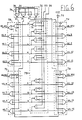
- Fig. 4 shows that correction circuit 8 comprises 4 banks 8A, ..., 8D of 5 registers, each register being constituted by 4 cells having the structure of Fig. 5 and storing a digit of information.
- register cell 9 comprises a FET (field effect transistor) switch 10 which, when switched on by signal CK1 at logical level 1, statically transfers the logical level of signal DOi at its data input to the loop constituted by the two NOT gates 11, 12.
- FET field effect transistor
- the cell is completed by two additional FET switches 13,14 series connected between ground and a voltage source +V through a pull-up resistor 15i.
- FET switch 13 is controlled by the signal on output Q or Q according to the preset (durihg manufacturing) of electrical connection T whilst FET switch 14, on whose drain is present data output signal CDOi, is controlled by signal SELj coming from decoder 7.
- CDOi signal will be at the same or inverted logical level of signal DOi depending on whether gate of switch 13 is connected to loop output Q or Q by connection T. This is equivalent to store a bit in direct or inverted form.
- Each output CDO 0-15 is connected to a voltage source +V through a pull-up resistor 15+0, ..., 15 ⁇ 15.
- each latching a portion of the data information the selection of the correct information or appropriate register is reconducted to the selection of the correct information or appropriate register within each bank, which selection may be performed in parallel on each bank.
- the syndrome decoder may be divided in a number of syndrome decoders equal to the number of register banks, but each decoder having to select a register in a number of registers which is lesser than the number of the information bits.
- This advantage may be further enhanced by a suitable selection of the data bits DI/DO 0 ⁇ 15 involved in the parity calculation to obtain CO-C5 and S0 ⁇ S5.
- the syndromes SO, S1 may be generated, so as to detect in which of the information digit a possible error exists, whilst syndromes S2, S3, S4 may be generated so as to detect, within the digit the bit affected by error.
- syndrome portion S2 S3 S4 may assume the same configuration for several data bits, the number of logic gates constituting decoder 7 can be reduced.
- syndrome decoder may be divided in the following major blocks.
- control gate sets are clocked by signal CK2, through inverter 7H, and only one control gate per set at a time is enabled, depending on signals received in input, to deliver a corresponding output signal SELj at logical level 1.
- Control gate set 7D further includes NOR gate 7L and control gate sets 7E, 7F, 7G further include inverters 7M, 7N, 7P respectively.
- the digit identification block 7A is composed of two NOT gates and four 2-input NAND gates.
- Level of signals D, E, F, G identifies which of the information digit is affected by error.
- each set 7D, 7E, 7F is enabled (through gates 7L, 7M, 7N respectively) to deliver selection signal SEL NE1, SEL NE2, SEL NE3 respectively, whilst the other gates in sets 7D, 7E, 7F are inhibited whatever is the level of syndromes S2, S3, S4.
- the "bit-within-digit" identification block 7B is composed of NAND gates, inverters, and one NOR gate 7R.
- one signal at a time can be at logic level 0 at the exclusion of the others.
- the register organization may range from N+1 registers, each having N cells, to 2N registers, each having 1 cell, and include any intermediate organization where any selected portion of the data information is stored in one independent register and for any selected portion further registers are provided to store any possible information obtained from the selected portion by inversion of one information bit.
- Obviously preferred partitioning are those which produces equal sized portions where the number of portions equals or approximates at best the number of bits in each portions so that the symptoms of the syndrome may be related in substantially equal number to the identification of the information portion where error is present, and to the identification of the error bit within the portion, thus minimizing complexity and propagation delay of the syndrome decoder.
Priority Applications (4)
| Application Number | Priority Date | Filing Date | Title |
|---|---|---|---|
| DE8484106012T DE3473365D1 (en) | 1984-05-26 | 1984-05-26 | Single error correction circuit for system memory |
| EP84106012A EP0162936B1 (en) | 1984-05-26 | 1984-05-26 | Single error correction circuit for system memory |
| US06/732,775 US4646304A (en) | 1984-05-26 | 1985-05-10 | Single error correction circuit for system memory |
| JP60113961A JPS6116351A (ja) | 1984-05-26 | 1985-05-27 | システムメモリ用単一誤り訂正回路 |
Applications Claiming Priority (1)
| Application Number | Priority Date | Filing Date | Title |
|---|---|---|---|
| EP84106012A EP0162936B1 (en) | 1984-05-26 | 1984-05-26 | Single error correction circuit for system memory |
Publications (2)
| Publication Number | Publication Date |
|---|---|
| EP0162936A1 EP0162936A1 (en) | 1985-12-04 |
| EP0162936B1 true EP0162936B1 (en) | 1988-08-10 |
Family
ID=8191954
Family Applications (1)
| Application Number | Title | Priority Date | Filing Date |
|---|---|---|---|
| EP84106012A Expired EP0162936B1 (en) | 1984-05-26 | 1984-05-26 | Single error correction circuit for system memory |
Country Status (4)
| Country | Link |
|---|---|
| US (1) | US4646304A (ja) |
| EP (1) | EP0162936B1 (ja) |
| JP (1) | JPS6116351A (ja) |
| DE (1) | DE3473365D1 (ja) |
Families Citing this family (24)
| Publication number | Priority date | Publication date | Assignee | Title |
|---|---|---|---|---|
| JP2515097B2 (ja) * | 1985-10-08 | 1996-07-10 | 日本テキサス・インスツルメンツ 株式会社 | 半導体記憶装置 |
| US4719627A (en) * | 1986-03-03 | 1988-01-12 | Unisys Corporation | Memory system employing a low DC power gate array for error correction |
| US4698812A (en) * | 1986-03-03 | 1987-10-06 | Unisys Corporation | Memory system employing a zero DC power gate array for error correction |
| US4866717A (en) * | 1986-07-29 | 1989-09-12 | Matsushita Electric Industrial Co., Ltd. | Code error detecting and correcting apparatus |
| US4805173A (en) * | 1986-09-15 | 1989-02-14 | Thinking Machines Corporation | Error control method and apparatus |
| IT1202527B (it) * | 1987-02-12 | 1989-02-09 | Honeywell Inf Systems | Sistema di memoria e relativo apparato di rivelazione-correzione di errore |
| EP0294678B1 (de) * | 1987-06-04 | 1992-03-11 | Siemens Nixdorf Informationssysteme Aktiengesellschaft | Sicherungseinrichtung zum Absichern von Daten in Speichereinheiten einer Datenverarbeitungsanlage unter Verwendung eines Fehlererkennungs- und Fehlerkorrekturcodes |
| US4905242A (en) * | 1987-06-09 | 1990-02-27 | The United States Of America As Represented By The Secretary Of The Air Force | Pipelined error detection and correction apparatus with programmable address trap |
| US4884271A (en) * | 1987-12-28 | 1989-11-28 | International Business Machines Corporation | Error checking and correcting for read-modified-write operations |
| JPH01196647A (ja) * | 1988-01-31 | 1989-08-08 | Nec Corp | 誤り訂正機能を有する記憶装置 |
| US4899342A (en) * | 1988-02-01 | 1990-02-06 | Thinking Machines Corporation | Method and apparatus for operating multi-unit array of memories |
| US4920539A (en) * | 1988-06-20 | 1990-04-24 | Prime Computer, Inc. | Memory error correction system |
| US5173905A (en) * | 1990-03-29 | 1992-12-22 | Micron Technology, Inc. | Parity and error correction coding on integrated circuit addresses |
| JPH04141900A (ja) * | 1990-10-01 | 1992-05-15 | Nec Ic Microcomput Syst Ltd | 半導体集積回路 |
| US5289477A (en) * | 1991-06-06 | 1994-02-22 | International Business Machines Corp. | Personal computer wherein ECC and partly error checking can be selectively chosen for memory elements installed in the system, memory elements enabling selective choice of error checking, and method |
| US5392292A (en) * | 1991-06-27 | 1995-02-21 | Cray Research, Inc. | Configurable spare memory chips |
| US7506226B2 (en) * | 2006-05-23 | 2009-03-17 | Micron Technology, Inc. | System and method for more efficiently using error correction codes to facilitate memory device testing |
| US8536430B2 (en) * | 2009-01-14 | 2013-09-17 | Geoffrey McCabe | Fine tuning means for fulcrum tremolo |
| FR2992504A1 (fr) * | 2012-06-26 | 2013-12-27 | Commissariat Energie Atomique | Dispositif et procede pour la correction d'erreurs dans un mot de code |
| US10002091B2 (en) * | 2015-03-26 | 2018-06-19 | Honeywell International Inc. | Master/slave management for redundant process controller modules |
| AU2019331448B2 (en) | 2018-08-29 | 2022-09-29 | Ecolab Usa Inc. | Use of multiple charged cationic compounds derived from primary amines or polyamines for microbial fouling control in a water system |
| US11084974B2 (en) | 2018-08-29 | 2021-08-10 | Championx Usa Inc. | Use of multiple charged cationic compounds derived from polyamines for clay stabilization in oil and gas operations |
| US11685709B2 (en) | 2018-08-29 | 2023-06-27 | Ecolab Usa Inc. | Multiple charged ionic compounds derived from polyamines and compositions thereof and use thereof as reverse emulsion breakers in oil and gas operations |
| US11640331B2 (en) * | 2021-07-29 | 2023-05-02 | Texas Instruments Incorporated | Securing physical layer startup from a low-power state |
Citations (1)
| Publication number | Priority date | Publication date | Assignee | Title |
|---|---|---|---|---|
| US4249253A (en) * | 1977-12-23 | 1981-02-03 | Honeywell Information Systems Italia | Memory with selective intervention error checking and correcting device |
Family Cites Families (11)
| Publication number | Priority date | Publication date | Assignee | Title |
|---|---|---|---|---|
| US4077565A (en) * | 1976-09-29 | 1978-03-07 | Honeywell Information Systems Inc. | Error detection and correction locator circuits |
| JPS5381036A (en) * | 1976-12-27 | 1978-07-18 | Hitachi Ltd | Error correction-detection system |
| US4255808A (en) * | 1979-04-19 | 1981-03-10 | Sperry Corporation | Hard or soft cell failure differentiator |
| US4319357A (en) * | 1979-12-14 | 1982-03-09 | International Business Machines Corp. | Double error correction using single error correcting code |
| US4319356A (en) * | 1979-12-19 | 1982-03-09 | Ncr Corporation | Self-correcting memory system |
| US4317201A (en) * | 1980-04-01 | 1982-02-23 | Honeywell, Inc. | Error detecting and correcting RAM assembly |
| US4380812A (en) * | 1980-04-25 | 1983-04-19 | Data General Corporation | Refresh and error detection and correction technique for a data processing system |
| US4359771A (en) * | 1980-07-25 | 1982-11-16 | Honeywell Information Systems Inc. | Method and apparatus for testing and verifying the operation of error control apparatus within a memory |
| JPS58123253A (ja) * | 1982-01-19 | 1983-07-22 | Sony Corp | エラ−訂正装置 |
| US4561095A (en) * | 1982-07-19 | 1985-12-24 | Fairchild Camera & Instrument Corporation | High-speed error correcting random access memory system |
| US4523314A (en) * | 1983-02-07 | 1985-06-11 | Sperry Corporation | Read error occurrence detector for error checking and correcting system |
-
1984
- 1984-05-26 EP EP84106012A patent/EP0162936B1/en not_active Expired
- 1984-05-26 DE DE8484106012T patent/DE3473365D1/de not_active Expired
-
1985
- 1985-05-10 US US06/732,775 patent/US4646304A/en not_active Expired - Fee Related
- 1985-05-27 JP JP60113961A patent/JPS6116351A/ja active Pending
Patent Citations (1)
| Publication number | Priority date | Publication date | Assignee | Title |
|---|---|---|---|---|
| US4249253A (en) * | 1977-12-23 | 1981-02-03 | Honeywell Information Systems Italia | Memory with selective intervention error checking and correcting device |
Also Published As
| Publication number | Publication date |
|---|---|
| DE3473365D1 (en) | 1988-09-15 |
| EP0162936A1 (en) | 1985-12-04 |
| JPS6116351A (ja) | 1986-01-24 |
| US4646304A (en) | 1987-02-24 |
Similar Documents
| Publication | Publication Date | Title |
|---|---|---|
| EP0162936B1 (en) | Single error correction circuit for system memory | |
| EP0172734A2 (en) | Semiconductor memory device | |
| US4747080A (en) | Semiconductor memory having self correction function | |
| US4730320A (en) | Semiconductor memory device | |
| US6549460B2 (en) | Memory device and memory card | |
| US4394763A (en) | Error-correcting system | |
| US5491703A (en) | Cam with additional row cells connected to match line | |
| US4612640A (en) | Error checking and correction circuitry for use with an electrically-programmable and electrically-erasable memory array | |
| US4345328A (en) | ECC Check bit generation using through checking parity bits | |
| US4456980A (en) | Semiconductor memory device | |
| EP0186719A1 (en) | Device for correcting errors in memories | |
| GB2034942A (en) | Errorcorrecting memory | |
| JPH11312396A (ja) | マルチビット半導体メモリ装置及びその装置の誤り訂正方法 | |
| US8201055B2 (en) | Semiconductor memory device | |
| JPS61267846A (ja) | メモリを有する集積回路装置 | |
| WO1983001523A1 (en) | Error-correcting memory with low storage overhead and fast correction mechanism | |
| US6438726B1 (en) | Method of dual use of non-volatile memory for error correction | |
| US6901552B1 (en) | System for storing data words in a RAM module | |
| US5337317A (en) | Minimizing the programming time in a semiconductor integrated memory circuit having an error correction function | |
| JPH03142800A (ja) | 電気的消去・書き込み可能なプログラマブル・リード・オンリー・メモリ | |
| SU982098A1 (ru) | Запоминающее устройство с исправлением ошибок | |
| SU849304A1 (ru) | Посто нное запоминающее устройство сКОРРЕКциЕй иНфОРМАции | |
| SU1278984A1 (ru) | Резервированное запоминающее устройство | |
| SU1161994A1 (ru) | Запоминающее устройство с автономным контролем | |
| SU1026165A1 (ru) | Запоминающее устройство с автономным контролем |
Legal Events
| Date | Code | Title | Description |
|---|---|---|---|
| PUAI | Public reference made under article 153(3) epc to a published international application that has entered the european phase |
Free format text: ORIGINAL CODE: 0009012 |
|
| 17P | Request for examination filed |
Effective date: 19850608 |
|
| AK | Designated contracting states |
Designated state(s): DE FR GB IT |
|
| 17Q | First examination report despatched |
Effective date: 19870326 |
|
| RAP1 | Party data changed (applicant data changed or rights of an application transferred) |
Owner name: HONEYWELL BULL ITALIA S.P.A. |
|
| GRAA | (expected) grant |
Free format text: ORIGINAL CODE: 0009210 |
|
| AK | Designated contracting states |
Kind code of ref document: B1 Designated state(s): DE FR GB IT |
|
| ITF | It: translation for a ep patent filed |
Owner name: HONEYWELL BULL ITALIA S.P.A |
|
| REF | Corresponds to: |
Ref document number: 3473365 Country of ref document: DE Date of ref document: 19880915 |
|
| ET | Fr: translation filed | ||
| PLBE | No opposition filed within time limit |
Free format text: ORIGINAL CODE: 0009261 |
|
| STAA | Information on the status of an ep patent application or granted ep patent |
Free format text: STATUS: NO OPPOSITION FILED WITHIN TIME LIMIT |
|
| 26N | No opposition filed | ||
| PGFP | Annual fee paid to national office [announced via postgrant information from national office to epo] |
Ref country code: DE Payment date: 19920413 Year of fee payment: 9 |
|
| PGFP | Annual fee paid to national office [announced via postgrant information from national office to epo] |
Ref country code: GB Payment date: 19920505 Year of fee payment: 9 |
|
| PGFP | Annual fee paid to national office [announced via postgrant information from national office to epo] |
Ref country code: FR Payment date: 19920521 Year of fee payment: 9 |
|
| PG25 | Lapsed in a contracting state [announced via postgrant information from national office to epo] |
Ref country code: GB Effective date: 19930526 |
|
| ITTA | It: last paid annual fee | ||
| GBPC | Gb: european patent ceased through non-payment of renewal fee |
Effective date: 19930526 |
|
| PG25 | Lapsed in a contracting state [announced via postgrant information from national office to epo] |
Ref country code: FR Effective date: 19940131 |
|
| PG25 | Lapsed in a contracting state [announced via postgrant information from national office to epo] |
Ref country code: DE Effective date: 19940201 |
|
| REG | Reference to a national code |
Ref country code: FR Ref legal event code: ST |