EP0157424B1 - LSI-Mikroprozessorbaustein mit rückwärts Kontaktstift-Kompatibilität - Google Patents
LSI-Mikroprozessorbaustein mit rückwärts Kontaktstift-Kompatibilität Download PDFInfo
- Publication number
- EP0157424B1 EP0157424B1 EP85104092A EP85104092A EP0157424B1 EP 0157424 B1 EP0157424 B1 EP 0157424B1 EP 85104092 A EP85104092 A EP 85104092A EP 85104092 A EP85104092 A EP 85104092A EP 0157424 B1 EP0157424 B1 EP 0157424B1
- Authority
- EP
- European Patent Office
- Prior art keywords
- chip
- functional
- section
- new
- compatibility
- Prior art date
- Legal status (The legal status is an assumption and is not a legal conclusion. Google has not performed a legal analysis and makes no representation as to the accuracy of the status listed.)
- Expired - Lifetime
Links
Images



Classifications
-
- G—PHYSICS
- G06—COMPUTING OR CALCULATING; COUNTING
- G06F—ELECTRIC DIGITAL DATA PROCESSING
- G06F1/00—Details not covered by groups G06F3/00 - G06F13/00 and G06F21/00
-
- G—PHYSICS
- G06—COMPUTING OR CALCULATING; COUNTING
- G06F—ELECTRIC DIGITAL DATA PROCESSING
- G06F12/00—Accessing, addressing or allocating within memory systems or architectures
- G06F12/02—Addressing or allocation; Relocation
- G06F12/06—Addressing a physical block of locations, e.g. base addressing, module addressing, memory dedication
- G06F12/0615—Address space extension
- G06F12/0623—Address space extension for memory modules
-
- G—PHYSICS
- G06—COMPUTING OR CALCULATING; COUNTING
- G06F—ELECTRIC DIGITAL DATA PROCESSING
- G06F1/00—Details not covered by groups G06F3/00 - G06F13/00 and G06F21/00
- G06F1/22—Means for limiting or controlling the pin/gate ratio
-
- G—PHYSICS
- G06—COMPUTING OR CALCULATING; COUNTING
- G06F—ELECTRIC DIGITAL DATA PROCESSING
- G06F15/00—Digital computers in general; Data processing equipment in general
Definitions
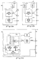
- the inverter circuit 12-240 together with NOR circuit 12-242, force signal T15E to the appropriate state in response to size comparator signal CMP. Also, NOR circuit 12-242 forces signal T15E to the appropriate state in response to address bit signal A22.
- These circuits in Figure 2d are logically represented by inputs CMP and A22.
- the NOR circuit 12-242 and inverter circuit 12-240 may take the form of the circuits described in the referenced text.
Landscapes
- Engineering & Computer Science (AREA)
- Theoretical Computer Science (AREA)
- Physics & Mathematics (AREA)
- General Engineering & Computer Science (AREA)
- General Physics & Mathematics (AREA)
- Computer Hardware Design (AREA)
- Microcomputers (AREA)
- Storage Device Security (AREA)
- Semiconductor Integrated Circuits (AREA)
Claims (9)
Applications Claiming Priority (2)
| Application Number | Priority Date | Filing Date | Title |
|---|---|---|---|
| US596756 | 1984-04-04 | ||
| US06/596,756 US4654789A (en) | 1984-04-04 | 1984-04-04 | LSI microprocessor chip with backward pin compatibility |
Publications (3)
| Publication Number | Publication Date |
|---|---|
| EP0157424A2 EP0157424A2 (de) | 1985-10-09 |
| EP0157424A3 EP0157424A3 (en) | 1986-10-29 |
| EP0157424B1 true EP0157424B1 (de) | 1990-08-29 |
Family
ID=24388572
Family Applications (1)
| Application Number | Title | Priority Date | Filing Date |
|---|---|---|---|
| EP85104092A Expired - Lifetime EP0157424B1 (de) | 1984-04-04 | 1985-04-04 | LSI-Mikroprozessorbaustein mit rückwärts Kontaktstift-Kompatibilität |
Country Status (9)
| Country | Link |
|---|---|
| US (1) | US4654789A (de) |
| EP (1) | EP0157424B1 (de) |
| KR (1) | KR910004311B1 (de) |
| AU (1) | AU578084B2 (de) |
| CA (1) | CA1226953A (de) |
| DE (1) | DE3579340D1 (de) |
| FI (1) | FI91813C (de) |
| MX (1) | MX163629B (de) |
| YU (1) | YU45982B (de) |
Families Citing this family (11)
| Publication number | Priority date | Publication date | Assignee | Title |
|---|---|---|---|---|
| US4876639A (en) * | 1983-09-20 | 1989-10-24 | Mensch Jr William D | Method and circuitry for causing sixteen bit microprocessor to execute eight bit op codes to produce either internal sixteen bit operation or internal eight bit operation in accordance with an emulation bit |
| KR0120930B1 (ko) * | 1987-12-01 | 1997-10-29 | 미다 가쓰시게 | 실행어드레스의 계산방법 및 통신제어장치 |
| US5163145A (en) * | 1989-04-25 | 1992-11-10 | Dell Usa L.P. | Circuit for determining between a first or second type CPU at reset by examining upper M bits of initial memory reference |
| US5373281A (en) * | 1991-08-15 | 1994-12-13 | Nartron Corporation | Failsafe module |
| US6000027A (en) * | 1992-08-25 | 1999-12-07 | Texas Instruments Incorporated | Method and apparatus for improved graphics/image processing using a processor and a memory |
| EP0613076A1 (de) * | 1993-01-27 | 1994-08-31 | National Semiconductor Corporation | Leiterplatterbehälter und IC Packung für vielfache oder einzige Versorgungsschaltungen |
| EP0881247B1 (de) * | 1997-05-29 | 2004-02-11 | Rohm And Haas Company | Vernetzte Polyaminsäure und deren Verfahren zur Herstellung |
| US6930473B2 (en) * | 2001-08-23 | 2005-08-16 | Fairchild Semiconductor Corporation | Method and circuit for reducing losses in DC-DC converters |
| US7650435B2 (en) * | 2004-10-22 | 2010-01-19 | International Business Machines Corporation | Apparatus and method to install a component in an information storage and retrieval system |
| KR101187642B1 (ko) * | 2011-05-02 | 2012-10-08 | 에스케이하이닉스 주식회사 | 집적 회로의 모니터링 장치 |
| US8855836B2 (en) * | 2012-06-21 | 2014-10-07 | Honeywell International Inc. | Methods and systems for implementing software-selectable multipurpose aircraft pins |
Family Cites Families (18)
| Publication number | Priority date | Publication date | Assignee | Title |
|---|---|---|---|---|
| US2706222A (en) * | 1952-05-22 | 1955-04-12 | Bell Telephone Labor Inc | Transistor lockout circuit |
| US4168537A (en) * | 1975-05-02 | 1979-09-18 | Tokyo Shibaura Electric Co., Ltd. | Nonvolatile memory system enabling nonvolatile data transfer during power on |
| US4159516A (en) * | 1976-03-23 | 1979-06-26 | Texas Instruments Incorporated | Input/output controller having selectable timing and maskable interrupt generation |
| US4074353A (en) * | 1976-05-24 | 1978-02-14 | Honeywell Information Systems Inc. | Trap mechanism for a data processing system |
| GB1595451A (en) * | 1976-11-26 | 1981-08-12 | Solartron Electronic Group | Multi function patch pin circuit |
| US4159541A (en) * | 1977-07-01 | 1979-06-26 | Ncr Corporation | Minimum pin memory device |
| US4145760A (en) * | 1978-04-11 | 1979-03-20 | Ncr Corporation | Memory device having a reduced number of pins |
| US4148099A (en) * | 1978-04-11 | 1979-04-03 | Ncr Corporation | Memory device having a minimum number of pins |
| US4375665A (en) * | 1978-04-24 | 1983-03-01 | Texas Instruments Incorporated | Eight bit standard connector bus for sixteen bit microcomputer using mirrored memory boards |
| US4163289A (en) * | 1978-05-01 | 1979-07-31 | Texas Instruments Incorporated | Sixteen bit microcomputer memory boards for use with eight bit standard connector bus |
| DE2824862A1 (de) * | 1978-06-06 | 1979-12-20 | Siemens Ag | Monolithisch integrierte digitale halbleiterschaltung |
| FR2431732A1 (fr) * | 1978-07-19 | 1980-02-15 | Materiel Telephonique | Dispositif de conversion d'adresse virtuelle en adresse reelle |
| US4500956A (en) * | 1978-07-21 | 1985-02-19 | Tandy Corporation | Memory addressing system |
| US4198698A (en) * | 1978-12-06 | 1980-04-15 | Fairchild Camera And Instrument Corporation | Chip select power-down control circuitry |
| US4340933A (en) * | 1979-02-12 | 1982-07-20 | Honeywell Information Systems Inc. | Data processing system having centralized nonexistent memory address detection |
| US4334268A (en) * | 1979-05-01 | 1982-06-08 | Motorola, Inc. | Microcomputer with branch on bit set/clear instructions |
| US4443864A (en) * | 1979-10-09 | 1984-04-17 | Texas Instruments Incorporated | Memory system for microprocessor with multiplexed address/data bus |
| US4441154A (en) * | 1981-04-13 | 1984-04-03 | Texas Instruments Incorporated | Self-emulator microcomputer |
-
1984
- 1984-04-04 US US06/596,756 patent/US4654789A/en not_active Expired - Lifetime
-
1985
- 1985-04-03 CA CA000478238A patent/CA1226953A/en not_active Expired
- 1985-04-03 AU AU40779/85A patent/AU578084B2/en not_active Ceased
- 1985-04-03 FI FI851331A patent/FI91813C/fi not_active IP Right Cessation
- 1985-04-04 YU YU56185A patent/YU45982B/sh unknown
- 1985-04-04 EP EP85104092A patent/EP0157424B1/de not_active Expired - Lifetime
- 1985-04-04 DE DE8585104092T patent/DE3579340D1/de not_active Expired - Lifetime
- 1985-04-04 KR KR1019850002284A patent/KR910004311B1/ko not_active Expired
- 1985-04-08 MX MX204870A patent/MX163629B/es unknown
Also Published As
| Publication number | Publication date |
|---|---|
| DE3579340D1 (de) | 1990-10-04 |
| KR910004311B1 (ko) | 1991-06-25 |
| FI91813C (fi) | 1994-08-10 |
| FI851331A0 (fi) | 1985-04-03 |
| MX163629B (es) | 1992-06-08 |
| EP0157424A2 (de) | 1985-10-09 |
| KR850007901A (ko) | 1985-12-09 |
| FI91813B (fi) | 1994-04-29 |
| YU56185A (en) | 1988-04-30 |
| AU4077985A (en) | 1985-10-10 |
| FI851331L (fi) | 1985-10-05 |
| EP0157424A3 (en) | 1986-10-29 |
| AU578084B2 (en) | 1988-10-13 |
| US4654789A (en) | 1987-03-31 |
| CA1226953A (en) | 1987-09-15 |
| YU45982B (sh) | 1992-12-21 |
Similar Documents
| Publication | Publication Date | Title |
|---|---|---|
| US4677548A (en) | LSI microprocessor chip with backward pin compatibility and forward expandable functionality | |
| US6363452B1 (en) | Method and apparatus for adding and removing components without powering down computer system | |
| EP0944959B1 (de) | Verfahren und vorrichtung zur wahl von m-ansteuerungsleitungen unter n-ansteuerungsleitungen | |
| US7266786B2 (en) | Method and apparatus for configurable address mapping and protection architecture and hardware for on-chip systems | |
| KR100366859B1 (ko) | Pci버스상에서이용되는디스크드라이브커넥터인터페이스 | |
| CN1126044C (zh) | 具有用于pci总线计算机的可编程配置寄存器的内插式板卡 | |
| US4654789A (en) | LSI microprocessor chip with backward pin compatibility | |
| US5958033A (en) | On- the-fly partitionable computer bus for enhanced operation with varying bus clock frequencies | |
| JP3866111B2 (ja) | 半導体集積回路及びバーンイン方法 | |
| US7103682B2 (en) | Apparatus and methods for transmitting data to a device having distributed configuration storage | |
| KR19990077461A (ko) | 컴퓨터시스템내의단일주변장치연결부(pci)호스트브리지에의해다수의pci버스를지원하는방법및시스템 | |
| EP0836141B1 (de) | Fehlertolerantes Bussystem | |
| US12013931B2 (en) | Method and system for freedom from interference (FFI) | |
| EP0013088B1 (de) | Hochintegrierte Halbleiterschaltung | |
| US20040158665A1 (en) | Reduced cardbus controller | |
| KR100265148B1 (ko) | 반도체 기판에 있어서 스위칭 전류 노이즈로부터 노이즈 센시티브 회로를 격리하는 방법 및 장치 | |
| US20220116038A1 (en) | Self-Gating Flops for Dynamic Power Reduction | |
| US6618828B1 (en) | Boundary scan testing involving shared enable latches | |
| US5576636A (en) | Low power programmable logic arrays | |
| US20050120155A1 (en) | Multi-bus I2C system | |
| US12321300B2 (en) | Apparatus and methods for translating transactions between one or more requesting units and a target unit | |
| EP0284060A2 (de) | Apparat zur Auswahl der Chipprüfbedingung | |
| US6519555B1 (en) | Apparatus and method of allowing PCI v1.0 devices to work in PCI v2.0 compliant system | |
| CN1006507B (zh) | 具有引腿向后兼容性和功能向前可扩性的大规模集成电路微处理机组件 | |
| GB2290640A (en) | Expanded I/O address space |
Legal Events
| Date | Code | Title | Description |
|---|---|---|---|
| PUAI | Public reference made under article 153(3) epc to a published international application that has entered the european phase |
Free format text: ORIGINAL CODE: 0009012 |
|
| AK | Designated contracting states |
Designated state(s): BE CH DE FR GB IT LI NL SE |
|
| RIN1 | Information on inventor provided before grant (corrected) |
Inventor name: BRADLEY, JOHN J. Inventor name: NUSINOV, EUGENE |
|
| PUAL | Search report despatched |
Free format text: ORIGINAL CODE: 0009013 |
|
| AK | Designated contracting states |
Kind code of ref document: A3 Designated state(s): BE CH DE FR GB IT LI NL SE |
|
| 17P | Request for examination filed |
Effective date: 19870408 |
|
| RAP1 | Party data changed (applicant data changed or rights of an application transferred) |
Owner name: HONEYWELL BULL INC. |
|
| 17Q | First examination report despatched |
Effective date: 19881107 |
|
| RAP1 | Party data changed (applicant data changed or rights of an application transferred) |
Owner name: BULL HN INFORMATION SYSTEMS INC. |
|
| GRAA | (expected) grant |
Free format text: ORIGINAL CODE: 0009210 |
|
| ITF | It: translation for a ep patent filed | ||
| AK | Designated contracting states |
Kind code of ref document: B1 Designated state(s): BE CH DE FR GB IT LI NL SE |
|
| REF | Corresponds to: |
Ref document number: 3579340 Country of ref document: DE Date of ref document: 19901004 |
|
| ET | Fr: translation filed | ||
| PLBI | Opposition filed |
Free format text: ORIGINAL CODE: 0009260 |
|
| 26 | Opposition filed |
Opponent name: SIEMENS AG GR PA 6 Effective date: 19910430 |
|
| NLR1 | Nl: opposition has been filed with the epo |
Opponent name: SIEMENS AG |
|
| PLBN | Opposition rejected |
Free format text: ORIGINAL CODE: 0009273 |
|
| STAA | Information on the status of an ep patent application or granted ep patent |
Free format text: STATUS: OPPOSITION REJECTED |
|
| 27O | Opposition rejected |
Effective date: 19921010 |
|
| K2C2 | Correction of patent specification (partial reprint) published |
Effective date: 19900829 |
|
| PGFP | Annual fee paid to national office [announced via postgrant information from national office to epo] |
Ref country code: FR Payment date: 19930329 Year of fee payment: 9 |
|
| PGFP | Annual fee paid to national office [announced via postgrant information from national office to epo] |
Ref country code: SE Payment date: 19930331 Year of fee payment: 9 Ref country code: GB Payment date: 19930331 Year of fee payment: 9 Ref country code: CH Payment date: 19930331 Year of fee payment: 9 |
|
| PGFP | Annual fee paid to national office [announced via postgrant information from national office to epo] |
Ref country code: DE Payment date: 19930401 Year of fee payment: 9 |
|
| NLR2 | Nl: decision of opposition | ||
| ITTA | It: last paid annual fee | ||
| PGFP | Annual fee paid to national office [announced via postgrant information from national office to epo] |
Ref country code: NL Payment date: 19930430 Year of fee payment: 9 |
|
| NLXE | Nl: other communications concerning ep-patents (part 3 heading xe) |
Free format text: ON 930310 A NEW PAGE 15 OF THE TRANSLATION OF THE PATENT SPECIFICATION HAS BEEN RECEIVED IN CONNECTION WITH A CORRECTION ISSUED BY THE EUROPEAN PATENT OFFICE |
|
| PGFP | Annual fee paid to national office [announced via postgrant information from national office to epo] |
Ref country code: BE Payment date: 19930506 Year of fee payment: 9 |
|
| PG25 | Lapsed in a contracting state [announced via postgrant information from national office to epo] |
Ref country code: GB Effective date: 19940404 |
|
| PG25 | Lapsed in a contracting state [announced via postgrant information from national office to epo] |
Ref country code: SE Effective date: 19940405 |
|
| PG25 | Lapsed in a contracting state [announced via postgrant information from national office to epo] |
Ref country code: LI Effective date: 19940430 Ref country code: CH Effective date: 19940430 Ref country code: BE Effective date: 19940430 |
|
| BERE | Be: lapsed |
Owner name: BULL HN INFORMATION SYSTEMS INC. Effective date: 19940430 |
|
| PG25 | Lapsed in a contracting state [announced via postgrant information from national office to epo] |
Ref country code: NL Effective date: 19941101 |
|
| GBPC | Gb: european patent ceased through non-payment of renewal fee |
Effective date: 19940404 |
|
| NLV4 | Nl: lapsed or anulled due to non-payment of the annual fee | ||
| PG25 | Lapsed in a contracting state [announced via postgrant information from national office to epo] |
Ref country code: FR Effective date: 19941229 |
|
| REG | Reference to a national code |
Ref country code: CH Ref legal event code: PL |
|
| PG25 | Lapsed in a contracting state [announced via postgrant information from national office to epo] |
Ref country code: DE Effective date: 19950103 |
|
| EUG | Se: european patent has lapsed |
Ref document number: 85104092.3 Effective date: 19941110 |
|
| REG | Reference to a national code |
Ref country code: FR Ref legal event code: ST |