EP0150829B1 - Optische Scheibe - Google Patents
Optische Scheibe Download PDFInfo
- Publication number
- EP0150829B1 EP0150829B1 EP85100780A EP85100780A EP0150829B1 EP 0150829 B1 EP0150829 B1 EP 0150829B1 EP 85100780 A EP85100780 A EP 85100780A EP 85100780 A EP85100780 A EP 85100780A EP 0150829 B1 EP0150829 B1 EP 0150829B1
- Authority
- EP
- European Patent Office
- Prior art keywords
- layer
- recording
- recording medium
- thin
- optical
- Prior art date
- Legal status (The legal status is an assumption and is not a legal conclusion. Google has not performed a legal analysis and makes no representation as to the accuracy of the status listed.)
- Expired
Links
- 230000003287 optical effect Effects 0.000 title claims description 45
- 239000010410 layer Substances 0.000 claims description 80
- 239000010408 film Substances 0.000 claims description 53
- 239000010409 thin film Substances 0.000 claims description 40
- 239000000758 substrate Substances 0.000 claims description 22
- 238000002310 reflectometry Methods 0.000 claims description 21
- 239000004065 semiconductor Substances 0.000 claims description 11
- 230000008033 biological extinction Effects 0.000 claims description 9
- 239000002356 single layer Substances 0.000 claims description 8
- 239000011241 protective layer Substances 0.000 claims description 6
- 229910052714 tellurium Inorganic materials 0.000 claims description 5
- 229910052732 germanium Inorganic materials 0.000 claims description 3
- GNPVGFCGXDBREM-UHFFFAOYSA-N germanium atom Chemical compound [Ge] GNPVGFCGXDBREM-UHFFFAOYSA-N 0.000 claims description 3
- PORWMNRCUJJQNO-UHFFFAOYSA-N tellurium atom Chemical compound [Te] PORWMNRCUJJQNO-UHFFFAOYSA-N 0.000 claims description 2
- 229910000927 Ge alloy Inorganic materials 0.000 claims 1
- 230000007246 mechanism Effects 0.000 description 12
- 239000000463 material Substances 0.000 description 10
- 230000008859 change Effects 0.000 description 7
- 229910052797 bismuth Inorganic materials 0.000 description 6
- 230000035945 sensitivity Effects 0.000 description 6
- 229910052751 metal Inorganic materials 0.000 description 5
- 239000002184 metal Substances 0.000 description 5
- 230000001681 protective effect Effects 0.000 description 4
- 239000007767 bonding agent Substances 0.000 description 3
- 238000009792 diffusion process Methods 0.000 description 3
- 229910052737 gold Inorganic materials 0.000 description 3
- 239000010931 gold Substances 0.000 description 3
- 239000004925 Acrylic resin Substances 0.000 description 2
- 229910021417 amorphous silicon Inorganic materials 0.000 description 2
- 230000005540 biological transmission Effects 0.000 description 2
- JCXGWMGPZLAOME-UHFFFAOYSA-N bismuth atom Chemical compound [Bi] JCXGWMGPZLAOME-UHFFFAOYSA-N 0.000 description 2
- 238000006243 chemical reaction Methods 0.000 description 2
- 239000011521 glass Substances 0.000 description 2
- PCHJSUWPFVWCPO-UHFFFAOYSA-N gold Chemical compound [Au] PCHJSUWPFVWCPO-UHFFFAOYSA-N 0.000 description 2
- 238000010438 heat treatment Methods 0.000 description 2
- 230000001678 irradiating effect Effects 0.000 description 2
- 229910052748 manganese Inorganic materials 0.000 description 2
- 238000004519 manufacturing process Methods 0.000 description 2
- 229920005668 polycarbonate resin Polymers 0.000 description 2
- 239000004431 polycarbonate resin Substances 0.000 description 2
- 230000005855 radiation Effects 0.000 description 2
- 239000011347 resin Substances 0.000 description 2
- 229920005989 resin Polymers 0.000 description 2
- 229910052711 selenium Inorganic materials 0.000 description 2
- 239000011669 selenium Substances 0.000 description 2
- 229910002899 Bi2Te3 Inorganic materials 0.000 description 1
- VGGSQFUCUMXWEO-UHFFFAOYSA-N Ethene Chemical compound C=C VGGSQFUCUMXWEO-UHFFFAOYSA-N 0.000 description 1
- 239000005977 Ethylene Substances 0.000 description 1
- BUGBHKTXTAQXES-UHFFFAOYSA-N Selenium Chemical compound [Se] BUGBHKTXTAQXES-UHFFFAOYSA-N 0.000 description 1
- XUIMIQQOPSSXEZ-UHFFFAOYSA-N Silicon Chemical compound [Si] XUIMIQQOPSSXEZ-UHFFFAOYSA-N 0.000 description 1
- 229910001215 Te alloy Inorganic materials 0.000 description 1
- 229910052782 aluminium Inorganic materials 0.000 description 1
- 229910052785 arsenic Inorganic materials 0.000 description 1
- 230000004888 barrier function Effects 0.000 description 1
- 229910052804 chromium Inorganic materials 0.000 description 1
- 239000011248 coating agent Substances 0.000 description 1
- 238000000576 coating method Methods 0.000 description 1
- 229910021419 crystalline silicon Inorganic materials 0.000 description 1
- 230000003247 decreasing effect Effects 0.000 description 1
- 230000007547 defect Effects 0.000 description 1
- 230000000694 effects Effects 0.000 description 1
- 239000012943 hotmelt Substances 0.000 description 1
- 230000006872 improvement Effects 0.000 description 1
- 229910052742 iron Inorganic materials 0.000 description 1
- 230000002427 irreversible effect Effects 0.000 description 1
- 239000004922 lacquer Substances 0.000 description 1
- 239000000155 melt Substances 0.000 description 1
- 238000002844 melting Methods 0.000 description 1
- 238000000034 method Methods 0.000 description 1
- 239000000203 mixture Substances 0.000 description 1
- 229910052750 molybdenum Inorganic materials 0.000 description 1
- 229910052759 nickel Inorganic materials 0.000 description 1
- 229910052758 niobium Inorganic materials 0.000 description 1
- 229910052763 palladium Inorganic materials 0.000 description 1
- 239000004033 plastic Substances 0.000 description 1
- 229910052697 platinum Inorganic materials 0.000 description 1
- 230000008569 process Effects 0.000 description 1
- 229910052703 rhodium Inorganic materials 0.000 description 1
- 229910052710 silicon Inorganic materials 0.000 description 1
- 239000010703 silicon Substances 0.000 description 1
- 229910052715 tantalum Inorganic materials 0.000 description 1
- 229910052721 tungsten Inorganic materials 0.000 description 1
- 229910052720 vanadium Inorganic materials 0.000 description 1
- 229910052725 zinc Inorganic materials 0.000 description 1
Images
Classifications
-
- G—PHYSICS
- G11—INFORMATION STORAGE
- G11B—INFORMATION STORAGE BASED ON RELATIVE MOVEMENT BETWEEN RECORD CARRIER AND TRANSDUCER
- G11B7/00—Recording or reproducing by optical means, e.g. recording using a thermal beam of optical radiation by modifying optical properties or the physical structure, reproducing using an optical beam at lower power by sensing optical properties; Record carriers therefor
- G11B7/24—Record carriers characterised by shape, structure or physical properties, or by the selection of the material
- G11B7/241—Record carriers characterised by shape, structure or physical properties, or by the selection of the material characterised by the selection of the material
- G11B7/252—Record carriers characterised by shape, structure or physical properties, or by the selection of the material characterised by the selection of the material of layers other than recording layers
- G11B7/257—Record carriers characterised by shape, structure or physical properties, or by the selection of the material characterised by the selection of the material of layers other than recording layers of layers having properties involved in recording or reproduction, e.g. optical interference layers or sensitising layers or dielectric layers, which are protecting the recording layers
-
- G—PHYSICS
- G11—INFORMATION STORAGE
- G11B—INFORMATION STORAGE BASED ON RELATIVE MOVEMENT BETWEEN RECORD CARRIER AND TRANSDUCER
- G11B7/00—Recording or reproducing by optical means, e.g. recording using a thermal beam of optical radiation by modifying optical properties or the physical structure, reproducing using an optical beam at lower power by sensing optical properties; Record carriers therefor
- G11B7/004—Recording, reproducing or erasing methods; Read, write or erase circuits therefor
- G11B7/0045—Recording
- G11B7/00455—Recording involving reflectivity, absorption or colour changes
-
- G—PHYSICS
- G11—INFORMATION STORAGE
- G11B—INFORMATION STORAGE BASED ON RELATIVE MOVEMENT BETWEEN RECORD CARRIER AND TRANSDUCER
- G11B7/00—Recording or reproducing by optical means, e.g. recording using a thermal beam of optical radiation by modifying optical properties or the physical structure, reproducing using an optical beam at lower power by sensing optical properties; Record carriers therefor
- G11B7/24—Record carriers characterised by shape, structure or physical properties, or by the selection of the material
- G11B7/2403—Layers; Shape, structure or physical properties thereof
- G11B7/24035—Recording layers
- G11B7/24038—Multiple laminated recording layers
-
- G—PHYSICS
- G11—INFORMATION STORAGE
- G11B—INFORMATION STORAGE BASED ON RELATIVE MOVEMENT BETWEEN RECORD CARRIER AND TRANSDUCER
- G11B7/00—Recording or reproducing by optical means, e.g. recording using a thermal beam of optical radiation by modifying optical properties or the physical structure, reproducing using an optical beam at lower power by sensing optical properties; Record carriers therefor
- G11B7/24—Record carriers characterised by shape, structure or physical properties, or by the selection of the material
- G11B7/241—Record carriers characterised by shape, structure or physical properties, or by the selection of the material characterised by the selection of the material
- G11B7/242—Record carriers characterised by shape, structure or physical properties, or by the selection of the material characterised by the selection of the material of recording layers
- G11B7/243—Record carriers characterised by shape, structure or physical properties, or by the selection of the material characterised by the selection of the material of recording layers comprising inorganic materials only, e.g. ablative layers
- G11B7/2433—Metals or elements of Groups 13, 14, 15 or 16 of the Periodic Table, e.g. B, Si, Ge, As, Sb, Bi, Se or Te
-
- G—PHYSICS
- G11—INFORMATION STORAGE
- G11B—INFORMATION STORAGE BASED ON RELATIVE MOVEMENT BETWEEN RECORD CARRIER AND TRANSDUCER
- G11B7/00—Recording or reproducing by optical means, e.g. recording using a thermal beam of optical radiation by modifying optical properties or the physical structure, reproducing using an optical beam at lower power by sensing optical properties; Record carriers therefor
- G11B7/24—Record carriers characterised by shape, structure or physical properties, or by the selection of the material
- G11B7/241—Record carriers characterised by shape, structure or physical properties, or by the selection of the material characterised by the selection of the material
- G11B7/242—Record carriers characterised by shape, structure or physical properties, or by the selection of the material characterised by the selection of the material of recording layers
- G11B7/243—Record carriers characterised by shape, structure or physical properties, or by the selection of the material characterised by the selection of the material of recording layers comprising inorganic materials only, e.g. ablative layers
- G11B2007/24302—Metals or metalloids
- G11B2007/24312—Metals or metalloids group 14 elements (e.g. Si, Ge, Sn)
-
- G—PHYSICS
- G11—INFORMATION STORAGE
- G11B—INFORMATION STORAGE BASED ON RELATIVE MOVEMENT BETWEEN RECORD CARRIER AND TRANSDUCER
- G11B7/00—Recording or reproducing by optical means, e.g. recording using a thermal beam of optical radiation by modifying optical properties or the physical structure, reproducing using an optical beam at lower power by sensing optical properties; Record carriers therefor
- G11B7/24—Record carriers characterised by shape, structure or physical properties, or by the selection of the material
- G11B7/241—Record carriers characterised by shape, structure or physical properties, or by the selection of the material characterised by the selection of the material
- G11B7/242—Record carriers characterised by shape, structure or physical properties, or by the selection of the material characterised by the selection of the material of recording layers
- G11B7/243—Record carriers characterised by shape, structure or physical properties, or by the selection of the material characterised by the selection of the material of recording layers comprising inorganic materials only, e.g. ablative layers
- G11B2007/24302—Metals or metalloids
- G11B2007/24314—Metals or metalloids group 15 elements (e.g. Sb, Bi)
-
- G—PHYSICS
- G11—INFORMATION STORAGE
- G11B—INFORMATION STORAGE BASED ON RELATIVE MOVEMENT BETWEEN RECORD CARRIER AND TRANSDUCER
- G11B7/00—Recording or reproducing by optical means, e.g. recording using a thermal beam of optical radiation by modifying optical properties or the physical structure, reproducing using an optical beam at lower power by sensing optical properties; Record carriers therefor
- G11B7/24—Record carriers characterised by shape, structure or physical properties, or by the selection of the material
- G11B7/241—Record carriers characterised by shape, structure or physical properties, or by the selection of the material characterised by the selection of the material
- G11B7/242—Record carriers characterised by shape, structure or physical properties, or by the selection of the material characterised by the selection of the material of recording layers
- G11B7/243—Record carriers characterised by shape, structure or physical properties, or by the selection of the material characterised by the selection of the material of recording layers comprising inorganic materials only, e.g. ablative layers
- G11B2007/24302—Metals or metalloids
- G11B2007/24316—Metals or metalloids group 16 elements (i.e. chalcogenides, Se, Te)
-
- G—PHYSICS
- G11—INFORMATION STORAGE
- G11B—INFORMATION STORAGE BASED ON RELATIVE MOVEMENT BETWEEN RECORD CARRIER AND TRANSDUCER
- G11B7/00—Recording or reproducing by optical means, e.g. recording using a thermal beam of optical radiation by modifying optical properties or the physical structure, reproducing using an optical beam at lower power by sensing optical properties; Record carriers therefor
- G11B7/24—Record carriers characterised by shape, structure or physical properties, or by the selection of the material
- G11B7/241—Record carriers characterised by shape, structure or physical properties, or by the selection of the material characterised by the selection of the material
- G11B7/252—Record carriers characterised by shape, structure or physical properties, or by the selection of the material characterised by the selection of the material of layers other than recording layers
- G11B7/253—Record carriers characterised by shape, structure or physical properties, or by the selection of the material characterised by the selection of the material of layers other than recording layers of substrates
- G11B7/2531—Record carriers characterised by shape, structure or physical properties, or by the selection of the material characterised by the selection of the material of layers other than recording layers of substrates comprising glass
-
- G—PHYSICS
- G11—INFORMATION STORAGE
- G11B—INFORMATION STORAGE BASED ON RELATIVE MOVEMENT BETWEEN RECORD CARRIER AND TRANSDUCER
- G11B7/00—Recording or reproducing by optical means, e.g. recording using a thermal beam of optical radiation by modifying optical properties or the physical structure, reproducing using an optical beam at lower power by sensing optical properties; Record carriers therefor
- G11B7/24—Record carriers characterised by shape, structure or physical properties, or by the selection of the material
- G11B7/241—Record carriers characterised by shape, structure or physical properties, or by the selection of the material characterised by the selection of the material
- G11B7/252—Record carriers characterised by shape, structure or physical properties, or by the selection of the material characterised by the selection of the material of layers other than recording layers
- G11B7/253—Record carriers characterised by shape, structure or physical properties, or by the selection of the material characterised by the selection of the material of layers other than recording layers of substrates
- G11B7/2533—Record carriers characterised by shape, structure or physical properties, or by the selection of the material characterised by the selection of the material of layers other than recording layers of substrates comprising resins
- G11B7/2534—Record carriers characterised by shape, structure or physical properties, or by the selection of the material characterised by the selection of the material of layers other than recording layers of substrates comprising resins polycarbonates [PC]
Definitions
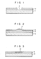
- the recording mechanism of conventional optical recording media is classified into the three categories shown in Figs. 1 to 3.
- a thin film 2 of a low-melting point material, such as Te or a Te alloy, and having a thickness of 20 to 80 nm is formed on a transparent substrate 1 of glass, polyacrylic resin, polycarbonate resin or the like. This film is irradiated with a laser beam, and its irradiated portion melts or evaporates, thereby forming a small pit 3. Thus, information is recorded.
- a low-melting point material such as Te or a Te alloy
- a gas-releasing film 5 and a metal film 6 are formed on a substrate 4.
- a gas is released in the irradiated portion of gas releasing film 5 by heat generated upon laser beam irradiation.
- the gas forms voids which result in raised blisters or bubbles 7 in the metal film 6, thereby recording information.
- the film 9 is irradiated with a laser beam.
- the irradiated portion has its structure changed. For example, this portion changes from a crystalline structure to an amorphous structure, thereby changing reflectance and recording information.
- the recording film evaporates or changes its shape.
- the recording sensitivity is degraded significantly. Therefore, to make practical use of these mechanisms, an air-sandwich structure must be adopted wherein the protective plate is arranged at a distance from the recording film. A disk of this complex structure is difficult to manufacture.
- the recording mechanism shown in Fig. 3 even if the protective film is formed directly on the recording film, the recording sensitivity will not be significantly decreased.
- this mechanism utilizes the structural change of the recording film, the boundary between recording and non-recording parts is unstable. Hence, the lifetime of the recorded data is short.
- Prior art document DE-A-25 36 264 discloses an information memory in which a recording layer consists of two layers having a barrier interposed therebetween.
- the two layers which form the recording layer are made of a material selected from the group consisting of Al, Se, Zn, Bi, As, Mn and In-Ga.
- prior art document "IBM Technical Disclosure Bulletin", Vol. 13, No. 10, March 1971, pages 3001-3002 discloses a beam writable and read-only memory structure consisting of a metal layer such as gold and amorphous semiconductor layer such as amorphous silicon which, upon local heating by an electron or optical beam, changes its optical characteristics from a previously heated state. After heating, the two layers form a mixture of gold, crystalline silicon and amorphous silicon.
- Prior art document DE-A-29 09 877 describes an optical recording medium for recording information comprising a substrate and a recording layer consisting of two films disposed on said substrate, wherein said two films can be melted by an incident laser radiation of a sufficient high intensity so as to form locally a data layer having another reflectivity.
- the recording layer consists of a Bi-film and a Te-film so that upon incident radiation Bi 2 Te 3 is obtained.
- prior art document US-A-3 560 994 describes a vaporizable recording medium in which a selenium layer, a bismuth layer, and a germanium layer are superposed on a transparent sheetlike carrier made of synthetic plastic material. To record information selected portions of the bismuth layer are exposed to a focused laser beam.
- the present invention provides an optical recording medium for recording information, comprising a substrate and a recording layer comprising two thin semiconductor film layers disposed on said substrate to form an optical disk, wherein areas of said thin semiconductor film layers can be selectively converted into a single layer when irradiated with a laser beam, thereby encoding information, said optical recording medium being characterized in that a first of said thin semiconductor film layers is made of germanium and the second thin film layer is made of tellurium.
- the materials of the thin film layers which can be converted into a single layer upon irradiation with a laser beam must be materials having different optical extinction coefficients.
- the recording layer comprises a bilayered body of two thin film layers having different optical extinction coefficients, irradiated portions of the thin film layers are converted into a single layer by mutual diffusion. The reflectivity at this portion is then changed from the rest of the film layers, thus recording information. The- information recorded in this manner is read out by irradiating the film layers with a laser beam having an intensity below a recording threshold intensity and by reading a difference in reflectivity.
- the ratio of the optical extinction coefficients of the bilayered recording layer is preferably set to be 1.5 or more. When this ratio is large, i.e. 1.5 or more, a change in reflectivity of the film layers upon conversion into a single layer is large and an optical recording medium having large reading signals can then be obtained.
- the thin film layers can be arranged in various ways. That is, a thin film layer having a larger or smaller optical extinction coefficient can be arranged at the incident side of a laser beam.
- the reflectivity is reduced.
- the reflectivity is increased. That is, in the latter case, if the initial reflectivity of the recording layer is low, the utilization effect of a laser beam is high.
- pulse noise occurring due to dark portions such as pinholes in the recording layer or scratches in the substrate can be easily separated from signals of recorded spots. Thus, a high S/N ratio can be obtained, and the latter arrangement is therefore preferable.
- the thin film layer at the incident side preferably has a thickness of 50 nm or less and the other film layer preferably has a thickness of 100 nm or less so as to provide excellent recording sensitivity.
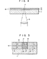
- the initial reflectivity Ri of this recording layer 12, i.e., the reflectivity before irradiation with a laser beam 15 having an intensity exceeding the threshold value for recording, is determined by the vector sum of the Fresnel's reflection coefficients r i , r 2 and r 3 at the boundaries between the substrate 11 and the first thin film 13, the first thin film 13 and the second thin film 14, and the second thin film 14 and an outside region 16.
- the vector length of each Fresnel's reflection coefficient is mainly determined by the complex indices of refraction n and r12 of the first and second thin films 13 and 14.
- the vector phase difference of the Fresnel's reflection coefficient is mainly determined by thicknesses d 1 and d 2 of the first and second thin films 13 and 14, respectively. Therefore, the initial reflectivity Ri can be freely set by properly selecting the materials of the first and second thin films 13 and 14 and the thicknesses d, and d 2 .
- recording of information is performed by local conversion of the reflectivity of the recording layer 12 from Ri to Rr by the above-mentioned mechanism.
- the information recorded in this manner is read out by detecting a change in reflectivity upon irradiating the layer with a laser beam spot of an intensity lower than the recording threshold intensity.
- the recording layer 12 to be used in the optical recording medium of the present invention must satisfy the following conditions: the recording threshold intensity of the laser beam is low, the ratio of the reflectivity Ri to Rr is large, and the first and second films 13 and 14 do not mutually diffuse at room temperature. These conditions are equivalent to conditions of high sensitivity, a high magnitude of the read out signal, and stability over a long period of time.
- a recording layer i.e., a recording layer consisting of a Te film and a Bi film, which already satisfies these conditions.
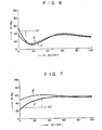
- Figs. 6 and 7 are graphs showing the relationship between the thickness d 1 of the first thin film 13 and the reflectivity Ri in the recording layer consisting of the Te and Bi films.
- Te has a complex index of refraction of 4.7-1.5i
- Bi has that of 1.7-3.3i.
- Fig. 6 shows the relationship between the thickness d 1 of the Te film and the reflectivity Ri when the inequality k, ⁇ k 2 is satisfied (where k, is the optical extinction coefficient of the first thin film 13 and k 2 is that of the second thin film 14) in order to satisfy Ri ⁇ Rr.
- solid line a and dotted line b respectively represent the cases wherein the thickness d 2 of the Bi film is 80 and 40 nm.
- a circle on the solid line a represents the value of Ri when the thickness of the Te film is 10 nm, and the arrow represents the change from Ri to Rr.
- Fig. 7 shows the relationship between the thickness d 1 and the reflectivity Ri' when the inequality k l >k 2 is satisfied in order to satisfy Ri'>Rr' and the first and second thin films respectively comprise Bi and Te films.
- solid line a' and dotted line b' respectively represent the cases wherein the thickness d 2 of the Te films is 80 and 40 nm.
- a circle on the solid line a' represents Ri' when the thickness of the Bi film is 30 nm, and the arrow shows change from Ri' to Rr'.
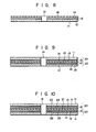
- two single- sided memory optical disks 20 each comprising a substrate 11 and a recording layer 12 consisting of thin films 13 and 14 are adhered through a bonding agent 21 to provide a double-sided memory optical disk.
- the bonding agent 21 can be a hot-melt type resin.
- the embodiment shown in Fig. 10 is a double-sided memory optical disk which is an improvement over that shown in Fig. 9.
- An undercoat 22 for modifying a surface defect is formed on each substrate 11.
- a protective layer 23 is formed on the surface of each recording layer 12 so as to prevent damage to the layer 12 during the bonding process of the two optical disks 20.
- the undercoat 22 can consist of a plasma-polymerized coating obtained by using ethylene or freon as a raw gas
- the protective layer 23 can consist of the same material as that of the protective layer 18 in the embodiment shown in Fig. 8.
- the recording layer 12 consists of two thin films 13 and 14.
- the recording layer 12 is irradiated with a spot of a laser beam 15, mutual diffusion of the films is locally caused and the films are converted into a single layer.
- the recording layer is not changed in shape, that is, no hole or expansion of the layer is caused for information recording. Therefore, even when the protective layers 18 or 23 are formed on the recording layer 12, or the disks 20 are adhered through the bonding agent 21, the recording sensitivity is not degraded and an inexpensive memory optical disk which is easy to handle can be provided.
- a first layer is made of Ge and a second layer is made of Te or Bi. The recorded information is stable and can be stored over a long period of time.
Landscapes
- Chemical & Material Sciences (AREA)
- Inorganic Chemistry (AREA)
- Optical Record Carriers And Manufacture Thereof (AREA)
- Thermal Transfer Or Thermal Recording In General (AREA)
Claims (7)
Applications Claiming Priority (2)
| Application Number | Priority Date | Filing Date | Title |
|---|---|---|---|
| JP59014058A JPS60160036A (ja) | 1984-01-28 | 1984-01-28 | 光デイスク |
| JP14058/84 | 1984-01-28 |
Publications (2)
| Publication Number | Publication Date |
|---|---|
| EP0150829A1 EP0150829A1 (de) | 1985-08-07 |
| EP0150829B1 true EP0150829B1 (de) | 1989-03-22 |
Family
ID=11850484
Family Applications (1)
| Application Number | Title | Priority Date | Filing Date |
|---|---|---|---|
| EP85100780A Expired EP0150829B1 (de) | 1984-01-28 | 1985-01-25 | Optische Scheibe |
Country Status (5)
| Country | Link |
|---|---|
| US (1) | US4682321A (de) |
| EP (1) | EP0150829B1 (de) |
| JP (1) | JPS60160036A (de) |
| KR (1) | KR900000017B1 (de) |
| DE (1) | DE3569054D1 (de) |
Families Citing this family (43)
| Publication number | Priority date | Publication date | Assignee | Title |
|---|---|---|---|---|
| JPS6222249A (ja) * | 1985-07-19 | 1987-01-30 | Matsushita Electric Ind Co Ltd | 光学式記録担体およびその製造方法 |
| DE3684306D1 (de) * | 1986-03-25 | 1992-04-16 | Toshiba Kawasaki Kk | Verfahren zum aufzeichnen von optischer information. |
| KR880002152A (ko) * | 1986-07-18 | 1988-04-29 | 나가이 아쯔시 | 광정보 기록디스크 |
| JPS63200331A (ja) * | 1987-02-13 | 1988-08-18 | Toshiba Corp | 記録媒体及び記録再生方法 |
| DE3884662T2 (de) * | 1987-05-08 | 1994-03-03 | Toshiba Kawasaki Kk | Medium für Informationsspeicherung. |
| DE4005315A1 (de) * | 1989-02-22 | 1990-08-23 | Toshiba Kawasaki Kk | Optisches informationsaufzeichnungsmedium |
| EP0394566A1 (de) * | 1989-04-28 | 1990-10-31 | Danismac S.A. | Optischer Aufzeichnungsträger |
| KR0146152B1 (ko) * | 1989-12-21 | 1998-10-15 | 이헌조 | 광기록매체 및 그 제조방법 |
| JP2808794B2 (ja) * | 1990-02-22 | 1998-10-08 | ソニー株式会社 | 両面光ディスク |
| US5101203A (en) * | 1990-06-29 | 1992-03-31 | International Business Machines Corporation | Digital data regeneration and deserialization circuits |
| US5255262A (en) * | 1991-06-04 | 1993-10-19 | International Business Machines Corporation | Multiple data surface optical data storage system with transmissive data surfaces |
| US5666344A (en) * | 1991-06-04 | 1997-09-09 | International Business Machines Corporation | Multiple data surface optical data storage system |
| TW218427B (de) * | 1991-06-04 | 1994-01-01 | Ibm | |
| US5586107A (en) * | 1991-06-04 | 1996-12-17 | International Business Machines Corporation | Multiple data surface optical data storage system |
| US5202875A (en) * | 1991-06-04 | 1993-04-13 | International Business Machines Corporation | Multiple data surface optical data storage system |
| US5449590A (en) * | 1991-06-04 | 1995-09-12 | International Business Machines Corporation | Multiple data surface optical data storage system |
| JP3170062B2 (ja) * | 1992-09-25 | 2001-05-28 | パイオニア株式会社 | 光ディスク |
| JP3400832B2 (ja) * | 1992-12-03 | 2003-04-28 | 株式会社日立製作所 | 情報記録媒体およびこれを用いた情報記録再生システム |
| EP0708962B1 (de) * | 1993-06-11 | 1999-10-20 | Kabushiki Kaisha Toshiba | Optiches aufzeichnungsmedium und speichersystem |
| JPH07141693A (ja) * | 1993-09-22 | 1995-06-02 | Toshiba Corp | 情報記録媒体 |
| GB9326508D0 (en) * | 1993-12-29 | 1994-03-02 | Johnson Matthey Plc | Data storage media |
| US5617088A (en) * | 1994-01-26 | 1997-04-01 | Sony Corporation | Sampling frequency converting device and memory address control device |
| US5644555A (en) * | 1995-01-19 | 1997-07-01 | International Business Machines Corporation | Multiple data surface magneto-optical data storage system |
| US5585158A (en) * | 1995-06-07 | 1996-12-17 | Eastman Kodak Company | Recordable optical element using low absorption materials |
| JPH09282710A (ja) * | 1996-04-15 | 1997-10-31 | Sony Corp | 光ディスクおよび光学的情報記録再生装置 |
| US6404708B1 (en) | 1998-09-30 | 2002-06-11 | Howard Hong-Dough Lee | Optical data-storage apparatus employing optical media with three-dimensional data pattern |
| FR2809856B1 (fr) * | 2000-05-30 | 2002-07-12 | Commissariat Energie Atomique | Supports d'enregistrement optique irreversible |
| CN1221962C (zh) * | 2002-04-26 | 2005-10-05 | Tdk股份有限公司 | 光记录介质和在其中对数据进行光记录的方法 |
| WO2003094161A1 (fr) * | 2002-04-30 | 2003-11-13 | Sony Corporation | Dispositif de fabrication d'un support optique d'enregistrement, et procede associe, support optique d'enregistrement, dispositif de reproduction et procede associe |
| US6996055B2 (en) | 2002-04-30 | 2006-02-07 | Tdk Corporation | Optical recording medium and method for optically recording data in the same |
| US7231649B2 (en) | 2002-05-31 | 2007-06-12 | Tdk Corporation | Optical recording medium and method for optically recording data in the same |
| JP4059714B2 (ja) | 2002-07-04 | 2008-03-12 | Tdk株式会社 | 光記録媒体 |
| JP4092147B2 (ja) * | 2002-07-04 | 2008-05-28 | Tdk株式会社 | 光記録媒体及び光記録方法 |
| JP4282285B2 (ja) * | 2002-08-12 | 2009-06-17 | Tdk株式会社 | 光記録媒体及び光記録方法 |
| US20040076907A1 (en) * | 2002-10-22 | 2004-04-22 | Tdk Corporation | Optical recording medium and method for manufacturing the same |
| US7781146B2 (en) * | 2002-11-22 | 2010-08-24 | Tdk Corporation | Optical recording medium |
| WO2004057594A1 (en) * | 2002-12-19 | 2004-07-08 | Koninklijke Philips Electronics N.V. | Use of bi-layer photolithographic resists as new material for optical storage |
| US7932015B2 (en) * | 2003-01-08 | 2011-04-26 | Tdk Corporation | Optical recording medium |
| JP2004355743A (ja) * | 2003-05-30 | 2004-12-16 | Tdk Corp | 光情報記録媒体 |
| JP2005044395A (ja) | 2003-07-23 | 2005-02-17 | Tdk Corp | 光情報記録媒体 |
| JP2005071402A (ja) | 2003-08-25 | 2005-03-17 | Tdk Corp | 光情報記録媒体 |
| EP2327074A4 (de) * | 2008-09-12 | 2016-12-21 | Univ Brigham Young | Datenspeichermedium mit carbon- und metallschichten |
| CN103770492B (zh) * | 2014-01-14 | 2015-05-20 | 汕头市龙湖昌丰化工有限公司 | 转移膜及转移镀铝纸的制作方法 |
Citations (3)
| Publication number | Priority date | Publication date | Assignee | Title |
|---|---|---|---|---|
| US3560994A (en) * | 1968-02-06 | 1971-02-02 | Bosch Gmbh Robert | Vaporizable recording medium |
| DE2909877A1 (de) * | 1978-03-16 | 1979-09-27 | Philips Nv | Verfahren, vorrichtung und aufzeichnungstraegerkoerper zum einschreiben von daten auf optischem wege |
| EP0068801A2 (de) * | 1981-06-22 | 1983-01-05 | International Business Machines Corporation | Optisches Speichermedium |
Family Cites Families (11)
| Publication number | Priority date | Publication date | Assignee | Title |
|---|---|---|---|---|
| JPS5420136B2 (de) * | 1974-07-09 | 1979-07-20 | ||
| US3959799A (en) * | 1974-09-09 | 1976-05-25 | International Business Machines Corporation | Information storage by laser beam initiated reactions |
| FR2365854A1 (fr) * | 1976-09-24 | 1978-04-21 | Thomson Brandt | Procede de fabrication d'un support d'information enregistrable et lisible optiquement et support obtenu par un tel procede |
| JPS5420137A (en) * | 1977-07-11 | 1979-02-15 | Kanesho Kk | Miticide |
| JPS5420136A (en) * | 1977-07-14 | 1979-02-15 | Kanae Kk | Stain proofing agent in water |
| US4195312A (en) * | 1978-02-24 | 1980-03-25 | Rca Corporation | Recorder and antireflective record blank having an optically passive transparent layer |
| NL7902542A (nl) * | 1979-04-02 | 1980-10-06 | Philips Nv | Optische registratie-inrichting met meerdere ablatieve registreerlagen. |
| JPS5722095A (en) * | 1980-07-15 | 1982-02-04 | Nec Corp | Laser beam recording material |
| US4519064A (en) * | 1980-10-27 | 1985-05-21 | Nippon Columbia Kabushikikaisha | Optical record disc |
| NL8202229A (nl) * | 1982-06-02 | 1984-01-02 | Docdata Bv | Medium voor het registreren van optisch uitleesbare informatie. |
| US4477819A (en) * | 1982-06-14 | 1984-10-16 | International Business Machines Corporation | Optical recording medium |
-
1984
- 1984-01-28 JP JP59014058A patent/JPS60160036A/ja active Pending
-
1985
- 1985-01-23 KR KR1019850000392A patent/KR900000017B1/ko not_active IP Right Cessation
- 1985-01-24 US US06/694,664 patent/US4682321A/en not_active Expired - Fee Related
- 1985-01-25 EP EP85100780A patent/EP0150829B1/de not_active Expired
- 1985-01-25 DE DE8585100780T patent/DE3569054D1/de not_active Expired
Patent Citations (3)
| Publication number | Priority date | Publication date | Assignee | Title |
|---|---|---|---|---|
| US3560994A (en) * | 1968-02-06 | 1971-02-02 | Bosch Gmbh Robert | Vaporizable recording medium |
| DE2909877A1 (de) * | 1978-03-16 | 1979-09-27 | Philips Nv | Verfahren, vorrichtung und aufzeichnungstraegerkoerper zum einschreiben von daten auf optischem wege |
| EP0068801A2 (de) * | 1981-06-22 | 1983-01-05 | International Business Machines Corporation | Optisches Speichermedium |
Also Published As
| Publication number | Publication date |
|---|---|
| JPS60160036A (ja) | 1985-08-21 |
| KR850005676A (ko) | 1985-08-28 |
| EP0150829A1 (de) | 1985-08-07 |
| DE3569054D1 (en) | 1989-04-27 |
| KR900000017B1 (ko) | 1990-01-18 |
| US4682321A (en) | 1987-07-21 |
Similar Documents
| Publication | Publication Date | Title |
|---|---|---|
| EP0150829B1 (de) | Optische Scheibe | |
| US6221455B1 (en) | Multi-layer optical disc and recording/reproducing apparatus | |
| US5194363A (en) | Optical recording medium and production process for the medium | |
| KR100770078B1 (ko) | 다층 광 디스크 | |
| US5817389A (en) | Optical disk | |
| US7276274B2 (en) | Optical recording medium and method for recording and reproducing data | |
| US4525412A (en) | Information recording medium | |
| US5208088A (en) | Optical recording medium | |
| KR20040035564A (ko) | 광기록매체 및 그 제조방법 | |
| JP2004158145A (ja) | 光記録媒体 | |
| EP1398767B1 (de) | Optisches Aufzeichnungs/Wiedergabeverfahren und optisches Aufzeichnungsmedium | |
| US6660451B1 (en) | Optical information recording medium | |
| US7682678B2 (en) | Optical information recording medium, recording and readout methods using the same, optical information recording device, and optical information readout device | |
| JP4619616B2 (ja) | 不可逆的光記録媒体 | |
| US20070009700A1 (en) | Optical recording medium | |
| JP2001023244A (ja) | 光記録媒体およびその製造方法と、光記録装置 | |
| JPH06243507A (ja) | 光情報キャリア | |
| JPH11250502A (ja) | 光ディスク | |
| US5449589A (en) | Method of making an optical information recording medium and method of recording/reproducing optical information | |
| JPH05298747A (ja) | 光学的情報記録媒体及びその構造設計方法 | |
| JP2000215516A (ja) | 光学的情報記録媒体とその製造方法、その記録再生方法および記録再生装置 | |
| JPH05298748A (ja) | 光学的情報記録媒体及びその構造設計方法 | |
| JP4083745B2 (ja) | 光記憶用新材料としての2層光転写レジストの利用 | |
| JP3313246B2 (ja) | 光学的情報記録媒体 | |
| JP4998224B2 (ja) | 光学的情報記録媒体 |
Legal Events
| Date | Code | Title | Description |
|---|---|---|---|
| PUAI | Public reference made under article 153(3) epc to a published international application that has entered the european phase |
Free format text: ORIGINAL CODE: 0009012 |
|
| 17P | Request for examination filed |
Effective date: 19850222 |
|
| AK | Designated contracting states |
Designated state(s): DE FR GB NL |
|
| GRAA | (expected) grant |
Free format text: ORIGINAL CODE: 0009210 |
|
| AK | Designated contracting states |
Kind code of ref document: B1 Designated state(s): DE FR GB NL |
|
| REF | Corresponds to: |
Ref document number: 3569054 Country of ref document: DE Date of ref document: 19890427 |
|
| ET | Fr: translation filed | ||
| PLBE | No opposition filed within time limit |
Free format text: ORIGINAL CODE: 0009261 |
|
| STAA | Information on the status of an ep patent application or granted ep patent |
Free format text: STATUS: NO OPPOSITION FILED WITHIN TIME LIMIT |
|
| 26N | No opposition filed | ||
| PGFP | Annual fee paid to national office [announced via postgrant information from national office to epo] |
Ref country code: FR Payment date: 19970109 Year of fee payment: 13 |
|
| PGFP | Annual fee paid to national office [announced via postgrant information from national office to epo] |
Ref country code: GB Payment date: 19970116 Year of fee payment: 13 |
|
| PGFP | Annual fee paid to national office [announced via postgrant information from national office to epo] |
Ref country code: NL Payment date: 19970130 Year of fee payment: 13 |
|
| PGFP | Annual fee paid to national office [announced via postgrant information from national office to epo] |
Ref country code: DE Payment date: 19970131 Year of fee payment: 13 |
|
| PG25 | Lapsed in a contracting state [announced via postgrant information from national office to epo] |
Ref country code: GB Free format text: LAPSE BECAUSE OF NON-PAYMENT OF DUE FEES Effective date: 19980125 |
|
| PG25 | Lapsed in a contracting state [announced via postgrant information from national office to epo] |
Ref country code: FR Free format text: THE PATENT HAS BEEN ANNULLED BY A DECISION OF A NATIONAL AUTHORITY Effective date: 19980131 |
|
| PG25 | Lapsed in a contracting state [announced via postgrant information from national office to epo] |
Ref country code: NL Free format text: LAPSE BECAUSE OF NON-PAYMENT OF DUE FEES Effective date: 19980801 |
|
| GBPC | Gb: european patent ceased through non-payment of renewal fee |
Effective date: 19980125 |
|
| NLV4 | Nl: lapsed or anulled due to non-payment of the annual fee |
Effective date: 19980801 |
|
| PG25 | Lapsed in a contracting state [announced via postgrant information from national office to epo] |
Ref country code: DE Free format text: LAPSE BECAUSE OF NON-PAYMENT OF DUE FEES Effective date: 19981001 |
|
| REG | Reference to a national code |
Ref country code: FR Ref legal event code: ST |