EP0147205A2 - Musterinspektion - Google Patents
Musterinspektion Download PDFInfo
- Publication number
- EP0147205A2 EP0147205A2 EP84308998A EP84308998A EP0147205A2 EP 0147205 A2 EP0147205 A2 EP 0147205A2 EP 84308998 A EP84308998 A EP 84308998A EP 84308998 A EP84308998 A EP 84308998A EP 0147205 A2 EP0147205 A2 EP 0147205A2
- Authority
- EP
- European Patent Office
- Prior art keywords
- pattern
- data
- original
- repeated
- scanning
- Prior art date
- Legal status (The legal status is an assumption and is not a legal conclusion. Google has not performed a legal analysis and makes no representation as to the accuracy of the status listed.)
- Granted
Links
Images


Classifications
-
- G—PHYSICS
- G06—COMPUTING OR CALCULATING; COUNTING
- G06T—IMAGE DATA PROCESSING OR GENERATION, IN GENERAL
- G06T7/00—Image analysis
- G06T7/0002—Inspection of images, e.g. flaw detection
- G06T7/0004—Industrial image inspection
- G06T7/001—Industrial image inspection using an image reference approach
-
- H—ELECTRICITY
- H10—SEMICONDUCTOR DEVICES; ELECTRIC SOLID-STATE DEVICES NOT OTHERWISE PROVIDED FOR
- H10P—GENERIC PROCESSES OR APPARATUS FOR THE MANUFACTURE OR TREATMENT OF DEVICES COVERED BY CLASS H10
- H10P95/00—Generic processes or apparatus for manufacture or treatments not covered by the other groups of this subclass
-
- G—PHYSICS
- G06—COMPUTING OR CALCULATING; COUNTING
- G06T—IMAGE DATA PROCESSING OR GENERATION, IN GENERAL
- G06T2207/00—Indexing scheme for image analysis or image enhancement
- G06T2207/30—Subject of image; Context of image processing
- G06T2207/30108—Industrial image inspection
- G06T2207/30148—Semiconductor; IC; Wafer
Definitions
- the present invention relates to pattern inspection.
- Patterns used in connection with recent VLSI's are almost entirely oriented towards high integration density and large capacity.
- a pattern generator etc. used to form such patterns, as many as 10 patterns are mounted on a single chip with an integration density of 5000 patterns/ mm 2 or more.
- inspection of high density patterning of a reticle, formed by a pattern generator on the basis of original data, or of a mask substrate or mask has often involved comparison and collation of a signal obtained by scanning the mask substrate and a signal of the same level obtained from the original data held on magnetic tape.
- an excessively great quantity (a countless number) of original data is involved.
- the present invention can provide a method of pattern inspection and pattern inspection apparatus which enables inspection to be carried out in a shorter time.
- the present invention can provide for a curtailment of the time required for inspecting patterning on a mask substrate for (for use in production of) a memory, and can afford simplification of apparatus for pattern inspection.
- the present invention provides a method of pattern inspection and pattern inspection apparatus capable of inspecting at a high speed a high density pattern having a repeated pattern portion for example like a mask substrate, such as a reticle or a mask used for a very large scale integration (VLSI) memory, etc.
- a mask substrate such as a reticle or a mask used for a very large scale integration (VLSI) memory, etc.
- VLSI very large scale integration
- a method of pattern inspection embodying the present invention involves comparison and collation of a signal obtained by scanning a mask substrate which carries high density patterning having a repeated pattern portion (a pattern portion wherein a basic pattern is repeated) and a signal obtained from original data designating or defining the patterning on the substrate, wherein pattern inspection data corresponding to the signal obtained by scanning the mask substrate and repeated basic pattern data corresponding to the basic pattern which is repeated in said repeated pattern portion are repeatedly compared and collated when inspection of said repeated pattern portion is effected, and wherein pattern inspection data and original pattern data, obtained by sequentially converting said original data in synchronization with said scanning, are compared and collated for inspection of areas of the high density patterning on the mask substrate other than said repeated pattern portion.
- Pattern inspection apparatus embodying the present invention for inspecting a mask substrate on which high density patterning having a repeated pattern portion is formed, on the basis of original data for the patterning, comprises:
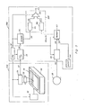
- the scanning part 100 includes a stage 24 for carrying a reticle or a mask substrate 10 which becomes a mask, a photo-electric converting part 26 which serves to convert an optical signal derived from the pattering on the mask substrate 10 into an electrical signal, an optical system 28 provided for an image sensor which works in cooperation with the photo-electric converting part 26, and a stage controller 30 which serves to control movement of the stage 24 in X and Y directions.
- the photo-electric converting part 26 and stage controller 30 are controlled by synchronous (synchronising) and control signals, etc. sent from a CPU 32.
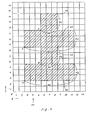
- Figure 4 is a schematic plan view illustrating how mask substrate 10 is scanned.
- the mask substrate 10 is placed on the stage 24 and is moved in X and Y directions.
- 54 indicates a region or zone which is viewed or sensed simultaneously by the image sensor (the field of view of the sensor). For example, a region as large as 1024 bits can be sensed, for example, in the direction Y.
- the mask substrate 10 is scanned from the one end to the other end with a width 56 - a scanning line (Y direction) width.
- the substrate is entirely scanned by movement (displacement) of such a scanning region or scanning line in the direction Y (e.g. ⁇ by scanning in a series of lines).
- the region (field of view) 54 for sensing by the image sensor comes on or encounters a pattern part 58 as shown in Figure 4 in the scanning region or scanning line illustrated.
- Figure 5 is a schematic diagram, to an enlarged scale as compared with Figure 4, showing a basic pattern described in more detail later and referred to here for assistance in explaining the pattern part 58 to which the basic pattern corresponds, as can be seen.
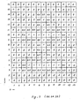
- the region 54 to be sensed by the image sensor (the field of view of the sensor) shown in Fig. 4 comes to the longitudinal area in the direction X among the bit section and the region 54 has the area of 16 bits for the simplification.
- the image sensor senses that the regions indicated by 1, 2, 6, 7, 8, 12, 16 bits in the direction Y (the bit elements identified by Y values 1, 2, 6, 7, 8, 12, 16 in the field of view column in Figure 5) are white patterns (pattern elements), while the regions indicated by 3 to 5 and 9 to 11 bits in the Y direction are black patterns (pattern elements).
- optical signals provided from the image sensor are output as an analog electrical signal, which is a pattern inspection signal Dl in Figure 3.
- Figure 6 illustrates the waveform of such a pattern inspection signal Dl.
- the two high levels in the waveform correspond to the black patterns (pattern elements) of the 3rd to 5th and 9th to llth bits in the Y direction in Figure 5.
- the pattern inspection signal Dl thus obtained is shaped and is converted into a digital signal bit by bit by A/D conversion means 34 seen in Figure 3.
- This provides (digital) pattern inspection data D2.
- the analog pattern inspection signal is sorted (divided) into white "0", grey "0.5” and black “1" data, depending upon the signal level being higher or lower than each of two levels V 1 and V 2 as shown in Figure 6.
- a signal level lower than level V 1 is defined as a white level
- a signal level between the levels V 1 and V 2 is defined as a grey level
- a signal level higher than the level V 2 is defined as a black level.
- pattern inspection data D2 corresponding to the pattern in the 13 x 16 bit region shown in Fig. 5 is obtained, the patterning indicated in Figure ' 7 can be obtained.
- Such (digital) pattern inspection data D2 is sequentially output (from the A/D converter 34) in accordance with the scanning operation and is stored in an inspected bit pattern memory means 36 of the main unit 200 in Figure 3.
- the pattern inspection data D2 shown in Figure 7 indicates data relating to a scanned region of 13 bits extent in the X direction.
- 38 is a magnetic tape which stores original data D3 which is equal to (the same as) that used by a pattern generator in order to form the patterning on the mask substrate 10.
- original data D3 employs a data base (a data format) suited to actual pattern formation, it is quite different from the pattern inspection signal Dl obtained by the image sensor and from the pattern inspection data D2 obtained by directly digitizing such signal Dl.
- a coordinate reference (6, 12), and width W d and height H d are stored. Namely, in respect of the 13 x 16 bit range shown in Figure 5, original data D3 as indicated by (3, 3), W a , H a , (6, 6), W b , H b , (3, 9), W c , H c , (6, 12), W d , H d ) is provided.
- the original data D3 is provided on a data base (in a form) suited to pattern formation and since it is not based on (bit elements) bit units such as picture elements, such data is not suitable for use in pattern inspection. Accordingly, the original data D3 is converted to data based on bit units (picture elements) by an original data conversion means 40.
- the original pattern data D4 obtained as a result of such conversion is data of the same kind as pattern inspection data D2 shown in Figure 7.
- Such a data conversion can be realized by determining whether a pertinent location corresponds to a white level "0", or a grey level "0.5” or a black level "1", with reference to the pattern data formed by the original data D3 for each bit position, but such conversion takes-time. -The presence of a grey level "0.5" can be determined, for.example, by the appliction of a rule such that a predetermined range between white and black regions is defined as grey.
- the original pattern data D4 output from the original data conversion means 40 is stored in original patten memory means 42 under.the control of CPU 32.
- the original data D3 sent from the magnetic tape 38 is sequentially converted into original pattern data D4, for each bit, in synchronization with scanning, in the original data conversion circuit 40 and is then temporarily stored in the original pattern memory 42.
- the pattern inspection signal Dl obtained from the scanning part 100 is converted to pattern inspection data D2 and the data D4 is compared and collated sequentially with the inspected pattern data D2, stored in the inspected pattern memory 36, by the comparator 300 and when a fault in patterning is detected on the basis of this comparison and collation an indication is provided at an output 52.
- the comparator 300 comprises a converter 46 which converts the pattern inspection data D2 into an inspected comparison signal D6, a converter 50 which converts the original pattern data D4 into an original comparison signal D7 and a comparator 50 which compares the signals D6 and D7.
- the signals D6 and D7 are of the same kind as shown in Figure 8. Namely, a "white” signal level corresponds to a .level 1, a "grey” signal -level corresponds to a level l 2 , and a "black” signal level corresponds to a level l 3 , respectively.
- Position along the horizontal axis (in the left to right direction) in Figure 8 corresponds equivalently to position along the horizontal axis (in the left to right direction) in Figure 6.
- repeated basic pattern data D5 corresponding to the basic pattern (e.g. data specifying the basic pattern itself without repeating) is input to the original pattern memory 42 from an input part 44, and the data D5 is repeatedly compared and collated with the pattern inspection data D2 by the comparator 300.
- the repeated basic pattern data D5 is data as illustrated in Figure 7, in a case in which the pattern indicated by the hatched area in Figure 5 is taken to be the basic pattern.
- the basic pattern is usually very much simpler than a random pattern, and therefore a long time is not required for the input of such basic pattern data. Moreover, since it is not required to sequentially convert original data D3 corresponding to the repeating of the basic pattern (to every repeat of the basic pattern) by the original data conversion means 40 in synchronisation with the scanning, the scanning speed of the scanning part 100 can be increased and thereby inspection time can be drastically curtailed. The reason for that is that it is not necessary to convert the data of each cell again and again and again.
- repeated basic pattern data D5 is input to the original pattern memory 42 from the input means 44.
- the present invention is not limited to these means.
- original data D3 concerning the basic pattern is input to the original data converter 40 from the magnetic tape 38, and then converted into the repeated basic pattern data J5, and then input to the original pattern memory 42.
- the data D5 is then repeatedly compared and collated.
- an output is partly modified and its is input to the original pattern memory 42,. in case at least one repeated basic pattern of outputs of A/D converter 34 is proved to be correct.
- the present invention provides a method for inspecting a pattern which compares and collates a signal obtained by scanning a mask substrate a high density pattern having a repeated pattern portion and a signal obtained from original data designating said high density pattern, comprising the steps of;
- the present invention also provides an apparatus which inspects a mask substrate allowing a high density pattern having a repeated pattern portion to be formed on the basis of an original data of said high density pattern, comprising:
- mask substrate used herein is employed also to designate a reticle, or a mask or any other suitable medium for bearing high density patterning to be inspected.
Landscapes
- Engineering & Computer Science (AREA)
- Quality & Reliability (AREA)
- Computer Vision & Pattern Recognition (AREA)
- Physics & Mathematics (AREA)
- General Physics & Mathematics (AREA)
- Theoretical Computer Science (AREA)
- Investigating Materials By The Use Of Optical Means Adapted For Particular Applications (AREA)
- Testing Or Measuring Of Semiconductors Or The Like (AREA)
- Preparing Plates And Mask In Photomechanical Process (AREA)
- Image Processing (AREA)
- Image Analysis (AREA)
Applications Claiming Priority (2)
| Application Number | Priority Date | Filing Date | Title |
|---|---|---|---|
| JP58249318A JPS60138924A (ja) | 1983-12-27 | 1983-12-27 | パタ−ン検査方法及びその装置 |
| JP249318/83 | 1983-12-27 |
Publications (3)
| Publication Number | Publication Date |
|---|---|
| EP0147205A2 true EP0147205A2 (de) | 1985-07-03 |
| EP0147205A3 EP0147205A3 (en) | 1987-08-26 |
| EP0147205B1 EP0147205B1 (de) | 1990-08-08 |
Family
ID=17191209
Family Applications (1)
| Application Number | Title | Priority Date | Filing Date |
|---|---|---|---|
| EP84308998A Expired EP0147205B1 (de) | 1983-12-27 | 1984-12-21 | Musterinspektion |
Country Status (5)
| Country | Link |
|---|---|
| US (1) | US4673816A (de) |
| EP (1) | EP0147205B1 (de) |
| JP (1) | JPS60138924A (de) |
| KR (1) | KR900001268B1 (de) |
| DE (1) | DE3482947D1 (de) |
Cited By (1)
| Publication number | Priority date | Publication date | Assignee | Title |
|---|---|---|---|---|
| FR2660772A1 (fr) * | 1990-04-10 | 1991-10-11 | Gerber Scientific Instr Co | Procede et appareil pour produire une base de donnees a trois etats destinee a etre utilisee avec des systemes automatiques de controle optique de circuits imprimes. |
Families Citing this family (8)
| Publication number | Priority date | Publication date | Assignee | Title |
|---|---|---|---|---|
| JPS6147635A (ja) * | 1984-08-14 | 1986-03-08 | Nippon Jido Seigyo Kk | パタ−ンの欠陥検査装置に用いるパタ−ンの判定方法 |
| JPS63111586A (ja) * | 1986-10-29 | 1988-05-16 | Hitachi Ltd | パタ−ン欠陥検査方法 |
| US5163128A (en) * | 1990-07-27 | 1992-11-10 | Gerber Systems Corporation | Method and apparatus for generating a multiple tolerance, three state data base for use with automatic optical inspection systems |
| JPH06222747A (ja) * | 1992-10-08 | 1994-08-12 | Fujitsu Isotec Ltd | フォント圧縮装置及びフォント復元装置 |
| US7561270B2 (en) | 2000-08-24 | 2009-07-14 | Asml Netherlands B.V. | Lithographic apparatus, device manufacturing method and device manufactured thereby |
| TW527526B (en) * | 2000-08-24 | 2003-04-11 | Asml Netherlands Bv | Lithographic apparatus, device manufacturing method, and device manufactured thereby |
| US7103750B2 (en) | 2003-03-20 | 2006-09-05 | International Business Machines Corporation | Method and apparatus for finding repeated substrings in pattern recognition |
| US7227994B2 (en) * | 2003-03-20 | 2007-06-05 | International Business Machines Corporation | Method and apparatus for imbedded pattern recognition using dual alternating pointers |
Family Cites Families (6)
| Publication number | Priority date | Publication date | Assignee | Title |
|---|---|---|---|---|
| DE2824849C2 (de) * | 1978-06-06 | 1982-12-16 | GAO Gesellschaft für Automation und Organisation mbH, 8000 München | Verfahren und Vorrichtung zur Feststellung des Zustandes und/oder der Echtheit von Blattgut |
| JPS5542013A (en) * | 1978-09-20 | 1980-03-25 | Hitachi Ltd | Automatic appearance test system |
| DE3070433D1 (en) * | 1980-12-18 | 1985-05-09 | Ibm | Method for the inspection and automatic sorting of objects with configurations of fixed dimensional tolerances, and device for carrying out the method |
| JPS57196530A (en) * | 1981-05-28 | 1982-12-02 | Fujitsu Ltd | Inspection of pattern |
| JPS57206025A (en) * | 1981-06-01 | 1982-12-17 | Fujitsu Ltd | Pattern inspecting system |
| JPH0750664B2 (ja) * | 1983-06-23 | 1995-05-31 | 富士通株式会社 | レチクルの検査方法 |
-
1983
- 1983-12-27 JP JP58249318A patent/JPS60138924A/ja active Pending
-
1984
- 1984-12-21 DE DE8484308998T patent/DE3482947D1/de not_active Expired - Lifetime
- 1984-12-21 EP EP84308998A patent/EP0147205B1/de not_active Expired
- 1984-12-26 KR KR1019840008342A patent/KR900001268B1/ko not_active Expired
- 1984-12-27 US US06/686,896 patent/US4673816A/en not_active Expired - Lifetime
Cited By (1)
| Publication number | Priority date | Publication date | Assignee | Title |
|---|---|---|---|---|
| FR2660772A1 (fr) * | 1990-04-10 | 1991-10-11 | Gerber Scientific Instr Co | Procede et appareil pour produire une base de donnees a trois etats destinee a etre utilisee avec des systemes automatiques de controle optique de circuits imprimes. |
Also Published As
| Publication number | Publication date |
|---|---|
| US4673816A (en) | 1987-06-16 |
| KR850005153A (ko) | 1985-08-21 |
| DE3482947D1 (de) | 1990-09-13 |
| KR900001268B1 (ko) | 1990-03-05 |
| EP0147205B1 (de) | 1990-08-08 |
| JPS60138924A (ja) | 1985-07-23 |
| EP0147205A3 (en) | 1987-08-26 |
Similar Documents
| Publication | Publication Date | Title |
|---|---|---|
| US4744047A (en) | Pattern test apparatus including a plurality of pattern generators | |
| CA1085514A (en) | Data compression system | |
| US4334274A (en) | Method of determining whether or not a region in a picture is within a closed boundary, and an apparatus therefor | |
| EP0166525A2 (de) | Pixel-zu-Vektor-Umwandlungsverfahren in einem automatischen Bildumsetzungssystem | |
| EP0309166A2 (de) | Bildverarbeitungssystem | |
| EP0147205A2 (de) | Musterinspektion | |
| US4700402A (en) | Input method for graphic pattern data | |
| JPH0139151B2 (de) | ||
| JPH1083452A (ja) | パターン欠陥検出装置 | |
| US4905144A (en) | High speed path optimization co-processor | |
| US4870693A (en) | Mask inspecting apparatus | |
| JP3119376B2 (ja) | 印字評価方法及び印字評価装置 | |
| JPH04229287A (ja) | 印字評価方法及び印字評価装置 | |
| US5577171A (en) | Figure pattern generating apparatus for detecting pattern defects | |
| JP3072787B2 (ja) | 印字評価方法及び印字評価装置 | |
| JP3072788B2 (ja) | 印字評価方法及び印字評価装置 | |
| JPH1074261A (ja) | パターン欠陥検出装置 | |
| JPH01205287A (ja) | 文字行傾き検出装置 | |
| JPH0564392B2 (de) | ||
| JPS60181880A (ja) | 光学的文字入力装置 | |
| KR840000665B1 (ko) | 광학식 판독장치 | |
| GB2119504A (en) | Non-contacting workpiece gauging system | |
| JPH1097634A (ja) | 物体の認識方法 | |
| JPH07113972B2 (ja) | 基準点検出方式 | |
| JPH04229759A (ja) | 印字評価方法及び印字評価装置 |
Legal Events
| Date | Code | Title | Description |
|---|---|---|---|
| PUAI | Public reference made under article 153(3) epc to a published international application that has entered the european phase |
Free format text: ORIGINAL CODE: 0009012 |
|
| AK | Designated contracting states |
Designated state(s): DE FR GB |
|
| PUAL | Search report despatched |
Free format text: ORIGINAL CODE: 0009013 |
|
| AK | Designated contracting states |
Kind code of ref document: A3 Designated state(s): DE FR GB |
|
| 17P | Request for examination filed |
Effective date: 19871030 |
|
| 17Q | First examination report despatched |
Effective date: 19890623 |
|
| GRAA | (expected) grant |
Free format text: ORIGINAL CODE: 0009210 |
|
| AK | Designated contracting states |
Kind code of ref document: B1 Designated state(s): DE FR GB |
|
| REF | Corresponds to: |
Ref document number: 3482947 Country of ref document: DE Date of ref document: 19900913 |
|
| ET | Fr: translation filed | ||
| PLBE | No opposition filed within time limit |
Free format text: ORIGINAL CODE: 0009261 |
|
| STAA | Information on the status of an ep patent application or granted ep patent |
Free format text: STATUS: NO OPPOSITION FILED WITHIN TIME LIMIT |
|
| 26N | No opposition filed | ||
| PGFP | Annual fee paid to national office [announced via postgrant information from national office to epo] |
Ref country code: DE Payment date: 20001211 Year of fee payment: 17 |
|
| PGFP | Annual fee paid to national office [announced via postgrant information from national office to epo] |
Ref country code: FR Payment date: 20001212 Year of fee payment: 17 |
|
| PGFP | Annual fee paid to national office [announced via postgrant information from national office to epo] |
Ref country code: GB Payment date: 20001220 Year of fee payment: 17 |
|
| PG25 | Lapsed in a contracting state [announced via postgrant information from national office to epo] |
Ref country code: GB Free format text: LAPSE BECAUSE OF NON-PAYMENT OF DUE FEES Effective date: 20011221 |
|
| REG | Reference to a national code |
Ref country code: GB Ref legal event code: IF02 |
|
| PG25 | Lapsed in a contracting state [announced via postgrant information from national office to epo] |
Ref country code: DE Free format text: LAPSE BECAUSE OF NON-PAYMENT OF DUE FEES Effective date: 20020702 |
|
| GBPC | Gb: european patent ceased through non-payment of renewal fee |
Effective date: 20011221 |
|
| PG25 | Lapsed in a contracting state [announced via postgrant information from national office to epo] |
Ref country code: FR Free format text: LAPSE BECAUSE OF NON-PAYMENT OF DUE FEES Effective date: 20020830 |
|
| REG | Reference to a national code |
Ref country code: FR Ref legal event code: ST |