EP0139990B1 - Reduced pressure epitaxial deposition process - Google Patents
Reduced pressure epitaxial deposition process Download PDFInfo
- Publication number
- EP0139990B1 EP0139990B1 EP84110058A EP84110058A EP0139990B1 EP 0139990 B1 EP0139990 B1 EP 0139990B1 EP 84110058 A EP84110058 A EP 84110058A EP 84110058 A EP84110058 A EP 84110058A EP 0139990 B1 EP0139990 B1 EP 0139990B1
- Authority
- EP
- European Patent Office
- Prior art keywords
- pressure
- autodoping
- deposition
- epitaxial deposition
- arsenic
- Prior art date
- Legal status (The legal status is an assumption and is not a legal conclusion. Google has not performed a legal analysis and makes no representation as to the accuracy of the status listed.)
- Expired
Links
- 238000005137 deposition process Methods 0.000 title claims description 6
- 238000000151 deposition Methods 0.000 claims description 29
- 238000002955 isolation Methods 0.000 claims description 19
- ZOXJGFHDIHLPTG-UHFFFAOYSA-N Boron Chemical compound [B] ZOXJGFHDIHLPTG-UHFFFAOYSA-N 0.000 claims description 17
- 229910052796 boron Inorganic materials 0.000 claims description 17
- 229910052785 arsenic Inorganic materials 0.000 claims description 16
- RQNWIZPPADIBDY-UHFFFAOYSA-N arsenic atom Chemical compound [As] RQNWIZPPADIBDY-UHFFFAOYSA-N 0.000 claims description 16
- 239000000758 substrate Substances 0.000 claims description 14
- 238000000034 method Methods 0.000 claims description 5
- XUIMIQQOPSSXEZ-UHFFFAOYSA-N Silicon Chemical compound [Si] XUIMIQQOPSSXEZ-UHFFFAOYSA-N 0.000 claims description 4
- 229910052710 silicon Inorganic materials 0.000 claims description 4
- 239000010703 silicon Substances 0.000 claims description 4
- VXEGSRKPIUDPQT-UHFFFAOYSA-N 4-[4-(4-methoxyphenyl)piperazin-1-yl]aniline Chemical compound C1=CC(OC)=CC=C1N1CCN(C=2C=CC(N)=CC=2)CC1 VXEGSRKPIUDPQT-UHFFFAOYSA-N 0.000 claims description 2
- 239000005049 silicon tetrachloride Substances 0.000 claims description 2
- 230000008021 deposition Effects 0.000 description 26
- 230000000694 effects Effects 0.000 description 4
- 239000012535 impurity Substances 0.000 description 4
- 150000002500 ions Chemical class 0.000 description 3
- 235000012431 wafers Nutrition 0.000 description 3
- UFHFLCQGNIYNRP-UHFFFAOYSA-N Hydrogen Chemical compound [H][H] UFHFLCQGNIYNRP-UHFFFAOYSA-N 0.000 description 2
- 239000001257 hydrogen Substances 0.000 description 2
- 229910052739 hydrogen Inorganic materials 0.000 description 2
- 238000012545 processing Methods 0.000 description 2
- 239000004065 semiconductor Substances 0.000 description 2
- 230000002411 adverse Effects 0.000 description 1
- RBFQJDQYXXHULB-UHFFFAOYSA-N arsane Chemical compound [AsH3] RBFQJDQYXXHULB-UHFFFAOYSA-N 0.000 description 1
- 230000015556 catabolic process Effects 0.000 description 1
- 230000003247 decreasing effect Effects 0.000 description 1
- 230000007547 defect Effects 0.000 description 1
- 238000006731 degradation reaction Methods 0.000 description 1
- 230000001419 dependent effect Effects 0.000 description 1
- 238000010586 diagram Methods 0.000 description 1
- 238000009792 diffusion process Methods 0.000 description 1
- 238000002474 experimental method Methods 0.000 description 1
- 239000007789 gas Substances 0.000 description 1
- 238000010348 incorporation Methods 0.000 description 1
- 238000010943 off-gassing Methods 0.000 description 1
- 238000012360 testing method Methods 0.000 description 1
Images

Classifications
-
- H—ELECTRICITY
- H01—ELECTRIC ELEMENTS
- H01L—SEMICONDUCTOR DEVICES NOT COVERED BY CLASS H10
- H01L21/00—Processes or apparatus adapted for the manufacture or treatment of semiconductor or solid state devices or of parts thereof
- H01L21/70—Manufacture or treatment of devices consisting of a plurality of solid state components formed in or on a common substrate or of parts thereof; Manufacture of integrated circuit devices or of parts thereof
- H01L21/71—Manufacture of specific parts of devices defined in group H01L21/70
- H01L21/74—Making of localized buried regions, e.g. buried collector layers, internal connections substrate contacts
-
- H—ELECTRICITY
- H01—ELECTRIC ELEMENTS
- H01L—SEMICONDUCTOR DEVICES NOT COVERED BY CLASS H10
- H01L21/00—Processes or apparatus adapted for the manufacture or treatment of semiconductor or solid state devices or of parts thereof
- H01L21/02—Manufacture or treatment of semiconductor devices or of parts thereof
- H01L21/02104—Forming layers
- H01L21/02365—Forming inorganic semiconducting materials on a substrate
- H01L21/02367—Substrates
- H01L21/0237—Materials
- H01L21/02373—Group 14 semiconducting materials
- H01L21/02381—Silicon, silicon germanium, germanium
-
- H—ELECTRICITY
- H01—ELECTRIC ELEMENTS
- H01L—SEMICONDUCTOR DEVICES NOT COVERED BY CLASS H10
- H01L21/00—Processes or apparatus adapted for the manufacture or treatment of semiconductor or solid state devices or of parts thereof
- H01L21/02—Manufacture or treatment of semiconductor devices or of parts thereof
- H01L21/02104—Forming layers
- H01L21/02365—Forming inorganic semiconducting materials on a substrate
- H01L21/02518—Deposited layers
- H01L21/02521—Materials
- H01L21/02524—Group 14 semiconducting materials
- H01L21/02532—Silicon, silicon germanium, germanium
-
- H—ELECTRICITY
- H01—ELECTRIC ELEMENTS
- H01L—SEMICONDUCTOR DEVICES NOT COVERED BY CLASS H10
- H01L21/00—Processes or apparatus adapted for the manufacture or treatment of semiconductor or solid state devices or of parts thereof
- H01L21/02—Manufacture or treatment of semiconductor devices or of parts thereof
- H01L21/02104—Forming layers
- H01L21/02365—Forming inorganic semiconducting materials on a substrate
- H01L21/02612—Formation types
- H01L21/02617—Deposition types
- H01L21/0262—Reduction or decomposition of gaseous compounds, e.g. CVD
-
- H—ELECTRICITY
- H01—ELECTRIC ELEMENTS
- H01L—SEMICONDUCTOR DEVICES NOT COVERED BY CLASS H10
- H01L21/00—Processes or apparatus adapted for the manufacture or treatment of semiconductor or solid state devices or of parts thereof
- H01L21/02—Manufacture or treatment of semiconductor devices or of parts thereof
- H01L21/04—Manufacture or treatment of semiconductor devices or of parts thereof the devices having potential barriers, e.g. a PN junction, depletion layer or carrier concentration layer
- H01L21/18—Manufacture or treatment of semiconductor devices or of parts thereof the devices having potential barriers, e.g. a PN junction, depletion layer or carrier concentration layer the devices having semiconductor bodies comprising elements of Group IV of the Periodic Table or AIIIBV compounds with or without impurities, e.g. doping materials
- H01L21/22—Diffusion of impurity materials, e.g. doping materials, electrode materials, into or out of a semiconductor body, or between semiconductor regions; Interactions between two or more impurities; Redistribution of impurities
- H01L21/2205—Diffusion of impurity materials, e.g. doping materials, electrode materials, into or out of a semiconductor body, or between semiconductor regions; Interactions between two or more impurities; Redistribution of impurities from the substrate during epitaxy, e.g. autodoping; Preventing or using autodoping
-
- Y—GENERAL TAGGING OF NEW TECHNOLOGICAL DEVELOPMENTS; GENERAL TAGGING OF CROSS-SECTIONAL TECHNOLOGIES SPANNING OVER SEVERAL SECTIONS OF THE IPC; TECHNICAL SUBJECTS COVERED BY FORMER USPC CROSS-REFERENCE ART COLLECTIONS [XRACs] AND DIGESTS
- Y10—TECHNICAL SUBJECTS COVERED BY FORMER USPC
- Y10S—TECHNICAL SUBJECTS COVERED BY FORMER USPC CROSS-REFERENCE ART COLLECTIONS [XRACs] AND DIGESTS
- Y10S438/00—Semiconductor device manufacturing: process
- Y10S438/914—Doping
- Y10S438/916—Autodoping control or utilization
Definitions
- This invention concerns a reduced pressure epitaxial deposition process and generally relates to bipolar transistor epitaxial deposition methods and, more particularly, to the selection of pressure during the epitaxial growth process to maximize bipolar device performance and leakage limited yield.
- the invention as claimed is intended to provide the desired teaching for an optimized epitaxial deposition process.
- epitaxial silicon is deposited upon a silicon substrate, having predetermined arsenic subcollector and boron isolation regions.
- the yield and performance enhancements are attributable to the minimization of arsenic and boron autodoping effects caused by the presence of the arsenic and boron regions in the substrate prior to epitaxial deposition.
- the prescribed deposition pressure values are predicated upon the use of optimized temperature, pressure and time prebake factors and source, growth rate and temperature deposition factors.
- bipolar semiconductor devices experience leakage limited yield and performance degradation due to autodoping effects when epitaxial layers are deposited upon semiconductor substrates containing subcollector and isolation regions.
- subcollector and isolation regions are placed into each substrate by separate ion implementation or diffusion steps, at predetermined localized areas.
- the subcollector region outdiffuses into the device area of the growing epitaxial layer and serves to provide a low ohmic collector contact region for the bipolar transistor which is later formed in the overlying epitaxial layer.
- the isolation region customarily lies beneath a recessed oxide region which surrounds each bipolar transistor to provide electrical isolation from other transistors.
- the isolation region ordinarily serves as a channel stop beneath the recessed oxide as is well known.
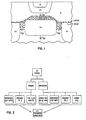
- FIG. 1 The cross sectional view of Fig. 1 is helpful in explaining the performance impact caused by boron and arsenic autodoping under various atmospheric-level pressure conditions for epitaxial deposition.
- Transistor performance is enhanced by lowering the two major capacitance components, collector-base capacitance (C CB ) and subcollector-isolation capacitance (C CS2 ).
- C CB collector-base capacitance
- C CS2 subcollector-isolation capacitance
- Lower epitaxial deposition pressure reduces the autodoping of n type impurities and thereby lowers the capacitance.
- C CB is determined by the electrically active arsenic (vertical autodoping) present between the base and the subcollector.
- the C CS2 capacitance is determined by the electrically active arsenic and boron between the p+ isolation and the subcollector (lateral autodoping). As the epitaxial deposition pressure is lowered, arsenic or n type autodoping is reduced, but the boron or p type autodoping is increased.
- prebake conditions are first optimized, while deposition conditions are held fixed, to enhance leakage limited yield and device performance.
- the parameters of interest are outlined in Fig. 2.
- Prebake refers to the processing of the substrate, having arsenic subcollectors and boron isolation regions therein, prior to epi deposition in an atmosphere of hydrogen.
- the specific pressure selected for a given substrate is dependent upon the subcollector-to-isolation area ratio embodied in the given substrate.
- silicon tetrachloride premixed with hydrogen is introduced into the epitaxial deposition chamber.
- Arsine is used to control the resistivity of the film in the range 0.1-0.3 0 cm.
- the growth rate is selected at a value within'the range from about 0.05 to about 0.5 pm per minute while the deposition temperature is set at a value in the range from about 1125°C to about 1150°C.
- the LLY penalty by using pressures below the cross-hatched pressure arise from boron autodoping causing base-to-isolation or base-to-collector leakage. This mechanism is shown in Fig. 4.
- the other factor limiting the value of the minimum pressure is out-gassing of trace metallic impurities and adsorbed gases (such as O2 and C0 2 ) from porous susceptors. This lowers leakage limited yields due to crystallographic defects appearing in the epitaxial films. This occurs typically below 80 Torr as shown in the plot in Fig. 3.
Landscapes
- Engineering & Computer Science (AREA)
- Physics & Mathematics (AREA)
- Condensed Matter Physics & Semiconductors (AREA)
- General Physics & Mathematics (AREA)
- Manufacturing & Machinery (AREA)
- Computer Hardware Design (AREA)
- Microelectronics & Electronic Packaging (AREA)
- Power Engineering (AREA)
- Chemical & Material Sciences (AREA)
- Materials Engineering (AREA)
- Bipolar Transistors (AREA)
Applications Claiming Priority (2)
| Application Number | Priority Date | Filing Date | Title |
|---|---|---|---|
| US543555 | 1983-10-19 | ||
| US06/543,555 US4504330A (en) | 1983-10-19 | 1983-10-19 | Optimum reduced pressure epitaxial growth process to prevent autodoping |
Publications (3)
| Publication Number | Publication Date |
|---|---|
| EP0139990A2 EP0139990A2 (en) | 1985-05-08 |
| EP0139990A3 EP0139990A3 (en) | 1985-08-28 |
| EP0139990B1 true EP0139990B1 (en) | 1989-01-25 |
Family
ID=24168529
Family Applications (1)
| Application Number | Title | Priority Date | Filing Date |
|---|---|---|---|
| EP84110058A Expired EP0139990B1 (en) | 1983-10-19 | 1984-08-23 | Reduced pressure epitaxial deposition process |
Country Status (4)
| Country | Link |
|---|---|
| US (1) | US4504330A (OSRAM) |
| EP (1) | EP0139990B1 (OSRAM) |
| JP (1) | JPS60101928A (OSRAM) |
| DE (1) | DE3476492D1 (OSRAM) |
Families Citing this family (4)
| Publication number | Priority date | Publication date | Assignee | Title |
|---|---|---|---|---|
| JPS63185061A (ja) * | 1987-01-28 | 1988-07-30 | Toshiba Corp | 半導体装置の製造方法 |
| JPH01161826A (ja) * | 1987-12-18 | 1989-06-26 | Toshiba Corp | 気相エピタキシャル成長法 |
| FR2766845B1 (fr) * | 1997-07-31 | 1999-10-15 | Sgs Thomson Microelectronics | Procede d'epitaxie sur un substrat de silicium comprenant des zones fortement dopees a l'arsenic |
| US6612240B1 (en) | 2000-09-15 | 2003-09-02 | Silverbrook Research Pty Ltd | Drying of an image on print media in a modular commercial printer |
Family Cites Families (4)
| Publication number | Priority date | Publication date | Assignee | Title |
|---|---|---|---|---|
| US3669769A (en) * | 1970-09-29 | 1972-06-13 | Ibm | Method for minimizing autodoping in epitaxial deposition |
| US3765960A (en) * | 1970-11-02 | 1973-10-16 | Ibm | Method for minimizing autodoping in epitaxial deposition |
| US4153486A (en) * | 1978-06-05 | 1979-05-08 | International Business Machines Corporation | Silicon tetrachloride epitaxial process for producing very sharp autodoping profiles and very low defect densities on substrates with high concentration buried impurity layers utilizing a preheating in hydrogen |
| US4263336A (en) * | 1979-11-23 | 1981-04-21 | Motorola, Inc. | Reduced pressure induction heated reactor and method |
-
1983
- 1983-10-19 US US06/543,555 patent/US4504330A/en not_active Expired - Fee Related
-
1984
- 1984-07-20 JP JP59149819A patent/JPS60101928A/ja active Granted
- 1984-08-23 DE DE8484110058T patent/DE3476492D1/de not_active Expired
- 1984-08-23 EP EP84110058A patent/EP0139990B1/en not_active Expired
Also Published As
| Publication number | Publication date |
|---|---|
| EP0139990A2 (en) | 1985-05-08 |
| EP0139990A3 (en) | 1985-08-28 |
| DE3476492D1 (en) | 1989-03-02 |
| JPH0526326B2 (OSRAM) | 1993-04-15 |
| JPS60101928A (ja) | 1985-06-06 |
| US4504330A (en) | 1985-03-12 |
Similar Documents
| Publication | Publication Date | Title |
|---|---|---|
| US6153920A (en) | Process for controlling dopant diffusion in a semiconductor layer and semiconductor device formed thereby | |
| US5273930A (en) | Method of forming a non-selective silicon-germanium epitaxial film | |
| US3861968A (en) | Method of fabricating integrated circuit device structure with complementary elements utilizing selective thermal oxidation and selective epitaxial deposition | |
| US3900345A (en) | Thin low temperature epi regions by conversion of an amorphous layer | |
| EP0430274A2 (en) | Method of producing bipolar transistor | |
| JPH0697666B2 (ja) | マルチレベル・エピタキシャル構造を用いた半導体デバイス構造体及びその製造方法 | |
| JPH04230037A (ja) | インサイチュ・ドープされたn型シリコン層の付着方法およびNPNトランジスタ | |
| US4437897A (en) | Fabrication process for a shallow emitter/base transistor using same polycrystalline layer | |
| EP0671770B1 (en) | Multilayer epitaxy for a silicon diode | |
| EP0148340B1 (en) | Ion etching process for deep trench etching multi-layer semiconductor substrates | |
| US6580104B1 (en) | Elimination of contaminants prior to epitaxy and related structure | |
| JP3079575B2 (ja) | 半導体装置の製造方法 | |
| US4618381A (en) | Method for adding impurities to semiconductor base material | |
| US3669769A (en) | Method for minimizing autodoping in epitaxial deposition | |
| JPH0437152A (ja) | 半導体装置の製造方法 | |
| EP0139990B1 (en) | Reduced pressure epitaxial deposition process | |
| US4164436A (en) | Process for preparation of semiconductor devices utilizing a two-step polycrystalline deposition technique to form a diffusion source | |
| US3765960A (en) | Method for minimizing autodoping in epitaxial deposition | |
| JP2911694B2 (ja) | 半導体基板及びその製造方法 | |
| JPH1041321A (ja) | バイポーラトランジスタの製造方法 | |
| US4128440A (en) | Liquid phase epitaxial method of covering buried regions for devices | |
| EP0289246A1 (en) | Method of manufacturing MOS devices | |
| JP2848404B2 (ja) | ▲iii▼―▲v▼族化合物半導体層の形成方法 | |
| GB1572819A (en) | Semiconductor device | |
| EP1116269B1 (en) | Complementary bipolar/cmos epitaxial structure and process |
Legal Events
| Date | Code | Title | Description |
|---|---|---|---|
| PUAI | Public reference made under article 153(3) epc to a published international application that has entered the european phase |
Free format text: ORIGINAL CODE: 0009012 |
|
| 17P | Request for examination filed |
Effective date: 19841123 |
|
| AK | Designated contracting states |
Designated state(s): DE FR GB |
|
| PUAL | Search report despatched |
Free format text: ORIGINAL CODE: 0009013 |
|
| AK | Designated contracting states |
Designated state(s): DE FR GB |
|
| 17Q | First examination report despatched |
Effective date: 19880426 |
|
| GRAA | (expected) grant |
Free format text: ORIGINAL CODE: 0009210 |
|
| AK | Designated contracting states |
Kind code of ref document: B1 Designated state(s): DE FR GB |
|
| REF | Corresponds to: |
Ref document number: 3476492 Country of ref document: DE Date of ref document: 19890302 |
|
| ET | Fr: translation filed | ||
| PLBE | No opposition filed within time limit |
Free format text: ORIGINAL CODE: 0009261 |
|
| STAA | Information on the status of an ep patent application or granted ep patent |
Free format text: STATUS: NO OPPOSITION FILED WITHIN TIME LIMIT |
|
| 26N | No opposition filed | ||
| PGFP | Annual fee paid to national office [announced via postgrant information from national office to epo] |
Ref country code: DE Payment date: 19920822 Year of fee payment: 9 |
|
| PGFP | Annual fee paid to national office [announced via postgrant information from national office to epo] |
Ref country code: GB Payment date: 19930720 Year of fee payment: 10 |
|
| PGFP | Annual fee paid to national office [announced via postgrant information from national office to epo] |
Ref country code: FR Payment date: 19930723 Year of fee payment: 10 |
|
| PG25 | Lapsed in a contracting state [announced via postgrant information from national office to epo] |
Ref country code: DE Effective date: 19940503 |
|
| PG25 | Lapsed in a contracting state [announced via postgrant information from national office to epo] |
Ref country code: GB Effective date: 19940823 |
|
| GBPC | Gb: european patent ceased through non-payment of renewal fee |
Effective date: 19940823 |
|
| PG25 | Lapsed in a contracting state [announced via postgrant information from national office to epo] |
Ref country code: FR Effective date: 19950428 |
|
| REG | Reference to a national code |
Ref country code: FR Ref legal event code: ST |