EP0136155A2 - Micro-ordinateur monopuce ayant des moyens pour empêcher la lecture de sa mémoire morte interne - Google Patents
Micro-ordinateur monopuce ayant des moyens pour empêcher la lecture de sa mémoire morte interne Download PDFInfo
- Publication number
- EP0136155A2 EP0136155A2 EP84306405A EP84306405A EP0136155A2 EP 0136155 A2 EP0136155 A2 EP 0136155A2 EP 84306405 A EP84306405 A EP 84306405A EP 84306405 A EP84306405 A EP 84306405A EP 0136155 A2 EP0136155 A2 EP 0136155A2
- Authority
- EP
- European Patent Office
- Prior art keywords
- external
- rom
- mode
- address
- chip microcomputer
- Prior art date
- Legal status (The legal status is an assumption and is not a legal conclusion. Google has not performed a legal analysis and makes no representation as to the accuracy of the status listed.)
- Granted
Links
Images


Classifications
-
- G—PHYSICS
- G06—COMPUTING; CALCULATING OR COUNTING
- G06F—ELECTRIC DIGITAL DATA PROCESSING
- G06F12/00—Accessing, addressing or allocating within memory systems or architectures
- G06F12/02—Addressing or allocation; Relocation
- G06F12/06—Addressing a physical block of locations, e.g. base addressing, module addressing, memory dedication
- G06F12/0615—Address space extension
- G06F12/0623—Address space extension for memory modules
-
- G—PHYSICS
- G06—COMPUTING; CALCULATING OR COUNTING
- G06F—ELECTRIC DIGITAL DATA PROCESSING
- G06F12/00—Accessing, addressing or allocating within memory systems or architectures
- G06F12/14—Protection against unauthorised use of memory or access to memory
-
- G—PHYSICS
- G06—COMPUTING; CALCULATING OR COUNTING
- G06F—ELECTRIC DIGITAL DATA PROCESSING
- G06F12/00—Accessing, addressing or allocating within memory systems or architectures
- G06F12/14—Protection against unauthorised use of memory or access to memory
- G06F12/1416—Protection against unauthorised use of memory or access to memory by checking the object accessibility, e.g. type of access defined by the memory independently of subject rights
- G06F12/1425—Protection against unauthorised use of memory or access to memory by checking the object accessibility, e.g. type of access defined by the memory independently of subject rights the protection being physical, e.g. cell, word, block
- G06F12/1433—Protection against unauthorised use of memory or access to memory by checking the object accessibility, e.g. type of access defined by the memory independently of subject rights the protection being physical, e.g. cell, word, block for a module or a part of a module
-
- G—PHYSICS
- G06—COMPUTING; CALCULATING OR COUNTING
- G06F—ELECTRIC DIGITAL DATA PROCESSING
- G06F12/00—Accessing, addressing or allocating within memory systems or architectures
- G06F12/02—Addressing or allocation; Relocation
- G06F12/06—Addressing a physical block of locations, e.g. base addressing, module addressing, memory dedication
- G06F12/0638—Combination of memories, e.g. ROM and RAM such as to permit replacement or supplementing of words in one module by words in another module
Definitions
- the present invention relates to a single-chip microcomputer, and more particularly, to a single-chip microcomputer having a means for preventing read-out of the contents of an internal ROM and thereby preventing fraudulent copying of its contents.
- a single chip microcomputer generally comprises an internal read-only memory, a program counter for generating an address, an interface port connectable to an external memory, and a switching means for switching, in response to a switching signal, between a first mode in which both the internal read-only memory and the external memory are used, and a second mode in which only the external memory is used.
- a single-chip microcomputer provided with an internal read-only memory (ROM) can be connected through an interface port to an external ROM.
- the external ROM usually has a first region in which the address space is different from that of the internal ROM for storing programs, and a second region in which the address space is equal to that of the internal ROM.
- the single-chip microcomputer when connected to an external ROM, can be used in a first mode of operation or a second mode of operation, in response to a switching signal, for example, an external access signal used when an external device is accessed.
- a switching signal for example, an external access signal used when an external device is accessed.
- the first mode of operation the internal ROM and the second region of the external ROM are accessible.
- the second mode of operation only the external ROM can be accessed unless a specific program such as later described in detail is stored in the external ROM.
- the contents of the internal ROM can be easily read out to equivalent addresses of the external portion by switching the external access signal to select the first mode of operation, and this can be achieved by a program stored in the second region of the external ROM.
- such a microcomputer includes an inhibiting means for inhibiting input of the switching signal into the switching means for switching from the second mode to the first mode when the address output from the program counter indicates an address in an address space other than the address space of the internal read-only memory.
- the program counter 3 generates an address of a memory to be accessed.
- the internal ROM 4 usually stores instructions and fixed data, and the manufacturer usually requires that these instructions or data in the internal ROM be kept secret.
- the interface port 5 is an interface circuit between the single-chip microcomputer 1 and an external ROM 8 which is provided for expanding the available address space of the single-chip microcomputer 1. At least a part of the address space of the external ROM 8 is identical to the address space of the internal ROM 4.
- the single-chip microcomputer 1 operates in either one of two modes of operations, i.e., a first mode and a second mode.
- the available memory region encompasses both the internal ROM 4 and the external ROM 8.
- the available memory region is only that of the external ROM 8, and the internal ROM 4 is not accessed unless a specific program is stored in the external ROM 8.
- the switching portion 6 switches between the first mode and the second mode, in response to, for example, a first external access signal EA.
- a first external access signal EA When the first external access signal EA is at logic "1", the switching portion 6 selects the first mode to output a first enable signal ENA 1 , which is applied to both the internal ROM 4 and the interface port 5.
- the switching portion 6 selects the second mode to output a second enable signal ENA 2 , which is applied only to the interface port 5.
- the inhibit circuit 7 is a flip-flop which receives at its data input D a second external access signal EAa and at its clock input C a reset signal RST.
- the second external access signal EA a can be generated automatically by the program stored in the internal ROM 4 or in the external ROM 8.
- the second external access signal EAa also can be manually applied by an operator.
- the reset signal RST is used to reset the program counter 3 or other modules (not shown) in the CPU 2.
- the reset signal RST is at logic "1"
- the second external access signal EXa is latched to be the first external access signal EA by the inhibit circuit 7. Therefore, during a period except for the reset period, the first external access signal EA is not changed. Accordingly, during the period except for the reset period, changing the mode of operation from the second mode to the first mode is inhibited.
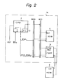
- FIG. 2 illustrates a conventional single-chip microcomputer.
- the inhibit circuit 7 is not provided in the single-chip microcomputer la, and the second external access signal EAa is directly input to the CPU 2.
- the problems arising in the conventional single-chip microcomputer la will now be explained with reference to Figures 2, 3A , 3B, 4, 5, 6A, and 6B.
- Figures 3A and 3B respectively, show available memory regions under the first and second modes of operation. That is, Figure 3A corresponds to the case when the external access signal EAa is at logic "1", wherein an internal ROM 4 having a capacity from an address #0000 to, for example, an address #OFFF (hexadecimal expression), and a first region 8-1 of the external ROM 8 from an address #1000 to an address #FFFF is utilized for processing. In this case, a restart address is the address #0000 of the internal ROM 1 and a second region 8-2 of the external ROM 8 is not accessed. The second region 8-2 of the external ROM 8 has the same address space as that of the internal ROM 4.
- an internal ROM 4 having a capacity from an address #0000 to, for example, an address #OFFF (hexadecimal expression)
- a first region 8-1 of the external ROM 8 from an address #1000 to an address #FFFF is utilized for processing.
- a restart address is the address #0000 of the internal ROM 1 and
- Figure 3B corresponds to the case when the signal EAa is at logic "0", wherein the second region 8-2 of the external ROM 8 from the address #0000 to the address #OFFF and the first region 8-1 of the external ROM 8 from the address #1000 to the address #FFFF are utilized for processing.
- the restart address is the address #0000 of the second region 8-2 of the external ROM 8 and the internal ROM 4 is not accessed unless a specific program is stored in the external ROM 8.
- the contents of the internal ROM 1 may be undesirably read-out to an external portion by, for example, a program in the first region 8-1 of the external ROM 8, in a mode as described later in conjunction with Figures 4, 5, 6A, and 6B.
- a program 80 as shown in Figure 4 is assumed to be provided in the external ROM 8.
- the operation executed by the program 80 is shown as a flow chart in Figure 5.
- the memory region used in the execution of the program is illustrated by slash lines in Figures 6A and 6B.
- steps 51 through 58 for reading the contents of the internal ROM 4 to an external portion.
- the external access signal EAa is set to "0" to execute the second mode of operation.
- the microcomputer la is reset.
- the restart address S 1 in this case is, as illustrated in Figure 6A, the address #0000 in the second region 8-2 of the external ROM 8.
- a jump instruction is executed to access an address S 2 in the first region 8-1 of the external ROM 8.
- the external access signal EAa is switched from "0" to "1" to execute the first mode of operation.
- the address S 2 should be more than OFFF, which is the maximum address in the second region 8-2 of the external ROM 8.
- a parameter i is set to be "0".
- the internal ROM 4 and the first region 8-1 of the external ROM 8 are utilized.
- a parameter i is set to be "0".
- the contents M(i) of the internal ROM 4 from its address #0000 to OFFF are read out to, for example, the external ROM 8 through the interface port 5.
- the symbol Pl represents the interface port 5 which receives the contents M(i).
- the addresses in which the contents of the internal ROM 4 are stored are represented by a symbol S 3
- the internal ROM 1 should contain a program which does not required access to the first region 8-1 of the external ROM 8.
- the program counter does not designate the first region 8-1 of the external ROM 8 during the first mode of operation. Therefore, in the first mode of operation also, the contents of the internal ROM 4 cannot be read out.
- Figure 7 illustrates another embodiment of the present invention.
- the flip-flop 7 shown in Figure 1 is shown in more detail.
- address signal A 12 through A 15 are employed in place of the reset signal RST.
- the address space of the external ROM 8 is, as shown in, for example, Figure 3B, from #0000 to #FFFF in hexadecimal expression. Each of the four characters in the hexadecimal expression can be broken down into 4 bits. Therefore, any address in the external ROM 8 can be expressed by sixteen bits A 0 through A 15 .
- the first region 8-1 of the external ROM 8 is more than or equal to the address #1000 in hexadecimal expression.
- the most significant character is expressed by the four bits A 12 through A 15 ; which is why the four bits A 12 through A 15 are employed.
- the four most significant bits A 12 through A 15 are applied to a NOR gate 10.
- the output of the NOR gate 10 is input as a clock signal to the flip-flop 7.
- the output Q of the flip-flop 7 is applied through an inverter 11 to another NOR gate 12.
- the NOR gate 12 also receives the four significant bits A 12 through A 15 .
- the output signal of the NOR gate 12 is applied as an enable signal ENA 1 to the internal ROM 4.
- the output Q of the flip-flop 7 is also applied to modules 13, which also utilize the external access signal EA.
- the flip-flop 7 includes inverters 71 and 72, AND gates 73 and 74 and OR gates 75 and 76.
- the available address space is from #0000 to #OFFF.
- the clock input C of the flip-flop 7 is "1"
- the first external access signal EA can be switched from “1” to "0” or "0" to "1” in response to the second external access signal.
- the available address space is also turned from the second region 8-2 of the external ROM 8 to the internal ROM 4, and therefore, the contents of the ROM 4 cannot be read out.
- the first external access signal EA is read out, and therefore, the contents of the internal ROM 4 cannot be read out.
- the memory regions of the internal ROM and the external ROM may be of any scale. Also, an external random-access memory (RAM) may be employed in place of the external ROM. Further, any other inhibiting means may be employed in place of the flip-flop 7.
- RAM random-access memory
Landscapes
- Engineering & Computer Science (AREA)
- Theoretical Computer Science (AREA)
- Physics & Mathematics (AREA)
- General Engineering & Computer Science (AREA)
- General Physics & Mathematics (AREA)
- Computer Security & Cryptography (AREA)
- Microcomputers (AREA)
- Storage Device Security (AREA)
- Memory System (AREA)
Applications Claiming Priority (2)
| Application Number | Priority Date | Filing Date | Title |
|---|---|---|---|
| JP175977/83 | 1983-09-22 | ||
| JP58175977A JPS6068441A (ja) | 1983-09-22 | 1983-09-22 | ワンチツプ・マイクロ・コンピユ−タ |
Publications (3)
| Publication Number | Publication Date |
|---|---|
| EP0136155A2 true EP0136155A2 (fr) | 1985-04-03 |
| EP0136155A3 EP0136155A3 (en) | 1986-12-17 |
| EP0136155B1 EP0136155B1 (fr) | 1989-11-15 |
Family
ID=16005545
Family Applications (1)
| Application Number | Title | Priority Date | Filing Date |
|---|---|---|---|
| EP84306405A Expired EP0136155B1 (fr) | 1983-09-22 | 1984-09-19 | Micro-ordinateur monopuce ayant des moyens pour empêcher la lecture de sa mémoire morte interne |
Country Status (5)
| Country | Link |
|---|---|
| US (1) | US5067077A (fr) |
| EP (1) | EP0136155B1 (fr) |
| JP (1) | JPS6068441A (fr) |
| KR (1) | KR890001312B1 (fr) |
| DE (1) | DE3480499D1 (fr) |
Cited By (8)
| Publication number | Priority date | Publication date | Assignee | Title |
|---|---|---|---|---|
| GB2163577A (en) * | 1984-08-23 | 1986-02-26 | Nat Res Dev | Software protection device |
| EP0229988A1 (fr) * | 1985-12-16 | 1987-07-29 | Siemens Aktiengesellschaft | Disposition de circuit pour bloquer la transmission de données à l'intérieur d'un appareil |
| FR2600795A1 (fr) * | 1986-06-27 | 1987-12-31 | Eurotechnique Sa | Procede de gestion d'un circuit electronique et circuit mettant en oeuvre un tel procede |
| EP0308219A2 (fr) * | 1987-09-18 | 1989-03-22 | General Instrument Corporation | Micro-ordinateur à sécurité de RAM interne pendant le mode de programme externe |
| EP0315209A2 (fr) * | 1987-11-05 | 1989-05-10 | Kabushiki Kaisha Toshiba | Micro-ordinateur avec mémoire |
| EP0502532A1 (fr) * | 1991-03-06 | 1992-09-09 | Nec Corporation | Microordinateur monopuce avec fonction de protection pour le contenu d'une mémoire morte interne |
| FR2674968A1 (fr) * | 1991-04-03 | 1992-10-09 | Samsung Electronics Co Ltd | Unite formant microcontroleur et comportant un dispositif d'acces a une memoire etendue. |
| GB2308905A (en) * | 1996-01-08 | 1997-07-09 | John Robert Miller | Protected system processor |
Families Citing this family (35)
| Publication number | Priority date | Publication date | Assignee | Title |
|---|---|---|---|---|
| JPH0738187B2 (ja) * | 1984-03-23 | 1995-04-26 | 株式会社日立製作所 | Lsiに構成されたマイクロコンピュータ |
| US5497482A (en) * | 1985-08-23 | 1996-03-05 | Hitachi, Ltd. | Data processor in which external sync signal may be selectively inhibited |
| JPH01184560A (ja) * | 1988-01-19 | 1989-07-24 | Nec Corp | シングルチップマイクロコンピュータ |
| DE3901457A1 (de) * | 1989-01-19 | 1990-08-02 | Strahlen Umweltforsch Gmbh | Verfahren zur adressbereichsueberwachung bei datenverarbeitungsgeraeten in echtzeit |
| US5263141A (en) * | 1989-01-31 | 1993-11-16 | Brother Kogyo Kabushiki Kaisha | Microprocessor with an exclusive address terminal for selecting at least one part of a peripheral device |
| JPH02202642A (ja) * | 1989-02-01 | 1990-08-10 | Toshiba Corp | プログラム動作監視装置 |
| JP2682700B2 (ja) * | 1989-05-09 | 1997-11-26 | 三菱電機株式会社 | Icカード |
| US5251304A (en) * | 1990-09-28 | 1993-10-05 | Motorola, Inc. | Integrated circuit microcontroller with on-chip memory and external bus interface and programmable mechanism for securing the contents of on-chip memory |
| DE4115152C2 (de) * | 1991-05-08 | 2003-04-24 | Gao Ges Automation Org | Kartenförmiger Datenträger mit einer datenschützenden Mikroprozessorschaltung |
| US5237669A (en) * | 1991-07-15 | 1993-08-17 | Quarterdeck Office Systems, Inc. | Memory management method |
| US5596755A (en) * | 1992-11-03 | 1997-01-21 | Microsoft Corporation | Mechanism for using common code to handle hardware interrupts in multiple processor modes |
| EP0601715A1 (fr) * | 1992-12-11 | 1994-06-15 | National Semiconductor Corporation | Bus de noyau CPV optimisé pour l'accès aux circuits de mémoire on-chip |
| US5426769A (en) * | 1993-08-26 | 1995-06-20 | Metalink Corp. | System and method for producing input/output expansion for single chip microcomputers |
| DE4340551A1 (de) * | 1993-11-29 | 1995-06-01 | Philips Patentverwaltung | Programmspeichererweiterung für einen Mikroprozessor |
| JP3520102B2 (ja) * | 1993-12-28 | 2004-04-19 | 株式会社東芝 | マイクロコンピュータ |
| JPH0855023A (ja) * | 1994-07-25 | 1996-02-27 | Motorola Inc | データ処理システムおよびその方法 |
| US5727005A (en) * | 1994-08-31 | 1998-03-10 | Le; Chinh H. | Integrated circuit microprocessor with programmable memory access interface types |
| WO1996008775A1 (fr) * | 1994-09-16 | 1996-03-21 | Philips Electronics N.V. | Systeme d'invalidation de bus programmable par logiciel |
| US5542044A (en) * | 1994-12-12 | 1996-07-30 | Pope; Shawn P. | Security device for a computer, and methods of constructing and utilizing same |
| US5644756A (en) * | 1995-04-07 | 1997-07-01 | Motorola, Inc. | Integrated circuit data processor with selectable routing of data accesses |
| JPH08305635A (ja) * | 1995-05-01 | 1996-11-22 | Nec Corp | ワンチップcpu |
| JPH0922385A (ja) * | 1995-07-05 | 1997-01-21 | Rohm Co Ltd | データセキュリティ装置および方法 |
| US5642480A (en) * | 1995-09-28 | 1997-06-24 | Motorola, Inc. | Method and apparatus for enhanced security of a data processor |
| US5737760A (en) * | 1995-10-06 | 1998-04-07 | Motorola Inc. | Microcontroller with security logic circuit which prevents reading of internal memory by external program |
| JP4312272B2 (ja) * | 1995-10-06 | 2009-08-12 | モトローラ・インコーポレイテッド | 内部メモリへのアクセスを制限するマイクロコントローラ |
| US6330648B1 (en) * | 1996-05-28 | 2001-12-11 | Mark L. Wambach | Computer memory with anti-virus and anti-overwrite protection apparatus |
| US5893923A (en) * | 1997-05-12 | 1999-04-13 | Lexmark International, Inc. | Microcontroller utilizing a circuit to select during reset process an internal or external memory as base memory |
| US6339815B1 (en) * | 1998-08-14 | 2002-01-15 | Silicon Storage Technology, Inc. | Microcontroller system having allocation circuitry to selectively allocate and/or hide portions of a program memory address space |
| US6505279B1 (en) | 1998-08-14 | 2003-01-07 | Silicon Storage Technology, Inc. | Microcontroller system having security circuitry to selectively lock portions of a program memory address space |
| FR2857535A1 (fr) * | 2003-07-09 | 2005-01-14 | Atmel Corp | Procede et systeme pour brouiller le contenu d'une cellule dans un circuit integre. |
| KR100636283B1 (ko) * | 2005-08-01 | 2006-10-18 | 삼성전자주식회사 | 외부저장매체를 이용한 메시지 처리 시스템 및 그 방법 |
| US20090158011A1 (en) * | 2007-12-14 | 2009-06-18 | Infineon Technologies Ag | Data processing system |
| US8819839B2 (en) | 2008-05-24 | 2014-08-26 | Via Technologies, Inc. | Microprocessor having a secure execution mode with provisions for monitoring, indicating, and managing security levels |
| US7788433B2 (en) * | 2008-05-24 | 2010-08-31 | Via Technologies, Inc. | Microprocessor apparatus providing for secure interrupts and exceptions |
| US9658793B2 (en) * | 2015-02-20 | 2017-05-23 | Qualcomm Incorporated | Adaptive mode translation lookaside buffer search and access fault |
Citations (2)
| Publication number | Priority date | Publication date | Assignee | Title |
|---|---|---|---|---|
| EP0072219A2 (fr) * | 1981-08-06 | 1983-02-16 | Kabushiki Kaisha Toshiba | Système d'adressage de mémoire |
| EP0109504A2 (fr) * | 1982-11-18 | 1984-05-30 | International Business Machines Corporation | Système de protection pour dispositifs de mémoire, d'entrée-sortie et équivalents |
Family Cites Families (11)
| Publication number | Priority date | Publication date | Assignee | Title |
|---|---|---|---|---|
| GB1540923A (en) * | 1975-12-01 | 1979-02-21 | Intel Corp | Programmable single chip mos computer |
| US4045782A (en) * | 1976-03-29 | 1977-08-30 | The Warner & Swasey Company | Microprogrammed processor system having external memory |
| JPS5757354A (en) * | 1980-09-24 | 1982-04-06 | Sharp Corp | Cut-off controller for internal memory |
| JPS57155642A (en) * | 1981-03-23 | 1982-09-25 | Nissan Motor Co Ltd | Computer capable of using correcting memory |
| JPS57174756A (en) * | 1981-04-21 | 1982-10-27 | Toshiba Corp | Controlling system for mode setting |
| US4368515A (en) * | 1981-05-07 | 1983-01-11 | Atari, Inc. | Bank switchable memory system |
| US4450524A (en) * | 1981-09-23 | 1984-05-22 | Rca Corporation | Single chip microcomputer with external decoder and memory and internal logic for disabling the ROM and relocating the RAM |
| JPS58109957A (ja) * | 1981-12-23 | 1983-06-30 | Nec Corp | シングルチツプマイクロコンピユ−タシステム |
| NL8201847A (nl) * | 1982-05-06 | 1983-12-01 | Philips Nv | Inrichting voor het beschermen tegen onbevoegd uitlezen van in een geheugen te memoriseren programmawoorden. |
| JPS6151695A (ja) * | 1984-08-22 | 1986-03-14 | Hitachi Ltd | 半導体集積回路装置 |
| US4698750A (en) * | 1984-12-27 | 1987-10-06 | Motorola, Inc. | Security for integrated circuit microcomputer with EEPROM |
-
1983
- 1983-09-22 JP JP58175977A patent/JPS6068441A/ja active Granted
-
1984
- 1984-09-19 EP EP84306405A patent/EP0136155B1/fr not_active Expired
- 1984-09-19 DE DE8484306405T patent/DE3480499D1/de not_active Expired
- 1984-09-19 KR KR1019840005730A patent/KR890001312B1/ko not_active IP Right Cessation
-
1991
- 1991-03-19 US US07/671,660 patent/US5067077A/en not_active Expired - Fee Related
Patent Citations (2)
| Publication number | Priority date | Publication date | Assignee | Title |
|---|---|---|---|---|
| EP0072219A2 (fr) * | 1981-08-06 | 1983-02-16 | Kabushiki Kaisha Toshiba | Système d'adressage de mémoire |
| EP0109504A2 (fr) * | 1982-11-18 | 1984-05-30 | International Business Machines Corporation | Système de protection pour dispositifs de mémoire, d'entrée-sortie et équivalents |
Non-Patent Citations (1)
| Title |
|---|
| ELECTRONIC DESIGN, vol. 26, no. 9, April 1978, pages 84-92, Rochell-Park, US; G. FIELLAND et al.: "Keep the memory interface simple between dynamic RAMs and a muP. Use the right timing and refresh, and you won't have to trade off much performance for cost" * |
Cited By (14)
| Publication number | Priority date | Publication date | Assignee | Title |
|---|---|---|---|---|
| US4634807A (en) * | 1984-08-23 | 1987-01-06 | National Research Development Corp. | Software protection device |
| GB2163577A (en) * | 1984-08-23 | 1986-02-26 | Nat Res Dev | Software protection device |
| EP0229988A1 (fr) * | 1985-12-16 | 1987-07-29 | Siemens Aktiengesellschaft | Disposition de circuit pour bloquer la transmission de données à l'intérieur d'un appareil |
| FR2600795A1 (fr) * | 1986-06-27 | 1987-12-31 | Eurotechnique Sa | Procede de gestion d'un circuit electronique et circuit mettant en oeuvre un tel procede |
| EP0255414A1 (fr) * | 1986-06-27 | 1988-02-03 | STMicroelectronics S.A. | Circuit intégré de protection à mémoire comprenant deux régions d'adresses sélectionnables |
| EP0308219A3 (fr) * | 1987-09-18 | 1990-09-05 | General Instrument Corporation | Micro-ordinateur à sécurité de RAM interne pendant le mode de programme externe |
| EP0308219A2 (fr) * | 1987-09-18 | 1989-03-22 | General Instrument Corporation | Micro-ordinateur à sécurité de RAM interne pendant le mode de programme externe |
| EP0315209A2 (fr) * | 1987-11-05 | 1989-05-10 | Kabushiki Kaisha Toshiba | Micro-ordinateur avec mémoire |
| EP0315209A3 (en) * | 1987-11-05 | 1990-07-11 | Kabushiki Kaisha Toshiba | Microcomputer incorporating memory |
| US5089951A (en) * | 1987-11-05 | 1992-02-18 | Kabushiki Kaisha Toshiba | Microcomputer incorporating memory |
| EP0502532A1 (fr) * | 1991-03-06 | 1992-09-09 | Nec Corporation | Microordinateur monopuce avec fonction de protection pour le contenu d'une mémoire morte interne |
| US5355466A (en) * | 1991-03-06 | 1994-10-11 | Nec Corporation | Single chip microcomputer having an address discrimination circuit and an operation mode terminal for protecting the content of internal ROM |
| FR2674968A1 (fr) * | 1991-04-03 | 1992-10-09 | Samsung Electronics Co Ltd | Unite formant microcontroleur et comportant un dispositif d'acces a une memoire etendue. |
| GB2308905A (en) * | 1996-01-08 | 1997-07-09 | John Robert Miller | Protected system processor |
Also Published As
| Publication number | Publication date |
|---|---|
| US5067077A (en) | 1991-11-19 |
| EP0136155A3 (en) | 1986-12-17 |
| JPS6068441A (ja) | 1985-04-19 |
| JPH0228179B2 (fr) | 1990-06-21 |
| KR890001312B1 (ko) | 1989-04-29 |
| DE3480499D1 (en) | 1989-12-21 |
| EP0136155B1 (fr) | 1989-11-15 |
| KR850002911A (ko) | 1985-05-20 |
Similar Documents
| Publication | Publication Date | Title |
|---|---|---|
| EP0136155A2 (fr) | Micro-ordinateur monopuce ayant des moyens pour empêcher la lecture de sa mémoire morte interne | |
| EP0127440B1 (fr) | Dispositif de circuit intégré incorporant une unité de traitement de données et une ROM mémorisant des programmes d'application | |
| US4694394A (en) | Microprocessor system having a multiplexed address/data bus which communicates with a plurality of memory and input/output devices including TTL output gates | |
| US5206938A (en) | Ic card with memory area protection based on address line restriction | |
| US4870562A (en) | Microcomputer capable of accessing internal memory at a desired variable access time | |
| US4777586A (en) | Semiconductor integrated circuit device with built-in arrangement for memory testing | |
| US4831522A (en) | Circuit and method for page addressing read only memory | |
| US5832251A (en) | Emulation device | |
| EP0518488A1 (fr) | Interface de bus et système de traitement | |
| US5019970A (en) | IC card | |
| US5016212A (en) | IC card having system ROM selection inhibit | |
| WO1997045870A1 (fr) | Microregisseur ayant une largeur de bus de donnees de n-bits et moins de n broches e/s et procede associe | |
| US4807185A (en) | Stack pointer control circuit | |
| EP0239283B1 (fr) | Microcalculateur | |
| US6219072B1 (en) | Microcomputer with a built in character display circuit and visual display unit using such a microcomputer | |
| EP0374733B1 (fr) | Microcalculateur sur une puce avec EPROM incorporé | |
| US6125054A (en) | Rom data read protect circuit | |
| US4967352A (en) | Data processor in which external sync signal may be selectively inhibited | |
| JPS6125173B2 (fr) | ||
| US6092148A (en) | Microcomputer having different memory capacities that can be selected from a common chip layout | |
| JPH0855097A (ja) | データ処理システム及びそのメモリアクセス方法 | |
| US5826059A (en) | Microcomputer for emulation | |
| US7191323B2 (en) | Information processing unit selecting one of reset vector addresses | |
| US5493686A (en) | Data processor in which external sync signal may be selectively inhibited | |
| JPS6329859A (ja) | 記憶保護装置 |
Legal Events
| Date | Code | Title | Description |
|---|---|---|---|
| PUAI | Public reference made under article 153(3) epc to a published international application that has entered the european phase |
Free format text: ORIGINAL CODE: 0009012 |
|
| AK | Designated contracting states |
Designated state(s): DE FR GB |
|
| RTI1 | Title (correction) | ||
| PUAL | Search report despatched |
Free format text: ORIGINAL CODE: 0009013 |
|
| AK | Designated contracting states |
Kind code of ref document: A3 Designated state(s): DE FR GB |
|
| 17P | Request for examination filed |
Effective date: 19870605 |
|
| 17Q | First examination report despatched |
Effective date: 19880308 |
|
| GRAA | (expected) grant |
Free format text: ORIGINAL CODE: 0009210 |
|
| AK | Designated contracting states |
Kind code of ref document: B1 Designated state(s): DE FR GB |
|
| REF | Corresponds to: |
Ref document number: 3480499 Country of ref document: DE Date of ref document: 19891221 |
|
| ET | Fr: translation filed | ||
| PLBE | No opposition filed within time limit |
Free format text: ORIGINAL CODE: 0009261 |
|
| STAA | Information on the status of an ep patent application or granted ep patent |
Free format text: STATUS: NO OPPOSITION FILED WITHIN TIME LIMIT |
|
| 26N | No opposition filed | ||
| PGFP | Annual fee paid to national office [announced via postgrant information from national office to epo] |
Ref country code: GB Payment date: 19920908 Year of fee payment: 9 |
|
| PGFP | Annual fee paid to national office [announced via postgrant information from national office to epo] |
Ref country code: FR Payment date: 19920929 Year of fee payment: 9 |
|
| PG25 | Lapsed in a contracting state [announced via postgrant information from national office to epo] |
Ref country code: GB Effective date: 19930919 |
|
| GBPC | Gb: european patent ceased through non-payment of renewal fee |
Effective date: 19930919 |
|
| PG25 | Lapsed in a contracting state [announced via postgrant information from national office to epo] |
Ref country code: FR Free format text: LAPSE BECAUSE OF NON-PAYMENT OF DUE FEES Effective date: 19940531 |
|
| REG | Reference to a national code |
Ref country code: FR Ref legal event code: ST |
|
| PGFP | Annual fee paid to national office [announced via postgrant information from national office to epo] |
Ref country code: DE Payment date: 19950928 Year of fee payment: 12 |
|
| PG25 | Lapsed in a contracting state [announced via postgrant information from national office to epo] |
Ref country code: DE Effective date: 19970603 |