EP0127488A2 - Verfahren zum Herstellen eines Leistungstransistors mit Spannungsbelastbarkeit beim Öffnen - Google Patents
Verfahren zum Herstellen eines Leistungstransistors mit Spannungsbelastbarkeit beim Öffnen Download PDFInfo
- Publication number
- EP0127488A2 EP0127488A2 EP84400562A EP84400562A EP0127488A2 EP 0127488 A2 EP0127488 A2 EP 0127488A2 EP 84400562 A EP84400562 A EP 84400562A EP 84400562 A EP84400562 A EP 84400562A EP 0127488 A2 EP0127488 A2 EP 0127488A2
- Authority
- EP
- European Patent Office
- Prior art keywords
- type
- concentration
- layer
- transistor
- intermediate zone
- Prior art date
- Legal status (The legal status is an assumption and is not a legal conclusion. Google has not performed a legal analysis and makes no representation as to the accuracy of the status listed.)
- Granted
Links
Images

Classifications
-
- H—ELECTRICITY
- H10—SEMICONDUCTOR DEVICES; ELECTRIC SOLID-STATE DEVICES NOT OTHERWISE PROVIDED FOR
- H10D—INORGANIC ELECTRIC SEMICONDUCTOR DEVICES
- H10D62/00—Semiconductor bodies, or regions thereof, of devices having potential barriers
- H10D62/10—Shapes, relative sizes or dispositions of the regions of the semiconductor bodies; Shapes of the semiconductor bodies
- H10D62/13—Semiconductor regions connected to electrodes carrying current to be rectified, amplified or switched, e.g. source or drain regions
- H10D62/137—Collector regions of BJTs
Definitions
- the present invention relates to the field of power transistors which can withstand high voltages, that is to say for example of the order of 500 to 1500 volts and relates more particularly to such transistors called to operate in switching regime, c '' i.e. by sudden passage from the conduction state to the blocking state and vice versa.
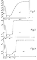
- Figures 1 to 3 characterize various types of conventional power transistors and represent on the ordinate the level of doping in the various layers of the transistor and on the abscissa the thickness of the transistor.
- FIG. 1 represents a transistor structure of the so-called triple diffused type. Starting from the collector electrode, there is successively an N + type collector contact area obtained by diffusion, an N type collector area corresponding to the initial substrate, a base P type area diffused in the substrate and a type N transmitter area. Orders of magnitude of doping and thickness of the various layers appear in the figure and correspond substantially to a transistor for which the collector / base breakdown voltage in open base is of the order of 1000 volts.
- N + type deep from the two faces of the substrate indeed, we do not know or we do not know how to mask one side of a substrate in the case of a long duration N type diffusion.
- the diffused area on one side of the wafer is removed, generally by running-in, and the basic and emitter diffusions are carried out.
- a first limitation of this manufacturing process results from the fact that it is not possible to economically form very deep diffused zones.
- the collector contact diffusions have a thickness of the order of 100 to 200 microns. Since the thicknesses of emitter, base and collector are well determined as a function of the desired characteristics of the transistor, for example of the order of 80 microns for the assembly in the case shown, we arrive at a thickness of wafer from 180 to 280 microns. However, a plate of this thickness has a certain mechanical fragility and is liable to be broken during the running-in operation or subsequent manipulations. Thus, this method is limited to cases where the treatment of platelets having a diameter of less than 10 cm is envisaged.
- FIG. 2 represents the simplest type of transistor with epitaxy collector.
- N type layer with low doping level for example 10 14 atoms / cm 3 in the illustrated case
- the thickness of the layer N + can be freely chosen and in particular has a thickness sufficient to exhibit mechanical strength adapted to the size of the insert.
- the base and emitter zones can be formed by any chosen methods which will not be detailed here since this is not the essential subject of the invention.
- these layers can be formed by ion implantation or even by epitaxy.
- FIG. 3 indicates a known variant of an epitaxial transistor.
- This collector layer is broken down into two successive epitaxial layers N and N1, the layer N1, on the substrate side, having a concentration of impurities higher than that of the collector layer proper.
- the two successive epitaxies can be formed in the same epitaxy frame by varying the dopant concentration during the process.
- This structure has various advantages, in particular of withstand voltage when switching on opening, compared to the structure in FIG. 2.
- the current theoretical explanations for this improvement in voltage withstand at switching on opening are based essentially on the fact that, in the case of FIG.
- the voltage withstand during switching at the opening of an epitaxial power transistor of the type illustrated in FIG. 2 and even of the type illustrated in FIG. 3 is relatively limited.
- An object of the present invention is to provide a method for manufacturing a power transistor with good switching resistance at opening which can be manufactured on plates. large area bowls.
- the present invention provides a method of manufacturing a power transistor withstanding high voltage at the opening consisting in: starting from a substrate of a first type of conductivity with high doping level; forming by epitaxy an intermediate zone of the first type of conductivity; forming by epitaxy a collector layer of the first type of conductivity at low doping level; then form a base layer of the second type of conductivity, then an emitter layer of the first type of conductivity.
- the intermediate zone has over its thickness a substantially constant concentration gradient of 20 to 40 microns per decade of concentration, the concentration of this intermediate zone being equal to that of the collector layer at this layer and increasing towards the substrate, the thickness of the intermediate zone being such that the concentration of the dopant drops by at least a decade over the thickness of this zone.
- the intermediate zone is obtained by continuously decreasing the dopant concentration during the epitaxy.
- the intermediate zone is obtained by carrying out successive epitaxial deposits of thin layers, the concentration of the dopant being reduced for each new layer and a smoothing of the concentration gradient being obtained during annealing later.
- FIG. 4 represents a power transistor structure according to the present invention.
- This transistor comprises an N + type substrate 10 followed by a zone 20 of the same type of conductivity, the concentration of which varies substantially continuously over about a decade of concentration (from 10 15 to 10 14 atoms / cm 3 in the example shown) to reach the concentration of the epitaxial collector layer 30 (10 14 atoms / cm 3 in the illustrated case).
- This transistor also conventionally comprises a P-type base area 40 formed by diffusion, then an N-type emitter area 50 also formed by diffusion.
- the concentration gradient of the intermediate zone 20 is chosen to be one decade for 20 to 40 microns thick (in other words half a decade to 20 microns thick).
- this intermediate zone 20 with a concentration gradient, it is possible to carry out an epitaxy from the substrate 10 by continuously varying the dopant concentration according to a determined rule in order to reach the chosen gradient or else to produce successive epitaxial layers of small thickness with decreasing dopant concentrations for each of the successive layers.
- a staircase structure is initially obtained and this staircase structure is greatly smoothed during subsequent annealing operations, in particular during the thermal operations necessary to effect the basic and emitter diffusions. .
- it may successively form five layers of a thickness of 5 to 7 microns respectively having concentrations of 10 15 a t polynomials / cm 3 8.10 14 atoms / cm 3 6.10 14 atoms / cm 3, 4.1014 has to my / cm 3 and 2.10 14 atoms / cm 3 ; natural redistribution during diffusions will then practically disappear the staircase steps.
- the safety area has the appearance of curve 2 in solid lines in FIG. 5.
- the maximum voltage that this transistor can withstand as soon as the collector current has a non-negligible value but not greater than approximately 0.5 I Cmax is around 70% of BV CEO ; but this voltage drops, as indicated by the rounded portion of the curve, when the current approaches the maximum current I Cmax which can only be supported for voltages below about 50X of BV CEO . Note a possibility of supporting higher voltages, close to BV CBO when the collector current is very low, but this is of little practical interest.
- the safety area changes notably in the case of a transistor according to the present invention, as represented by the curve 4 in dotted lines in FIG. 5.
- the value BV CEO does not constitute a particular limitation of the security area.
- the transistor can withstand a voltage close to BV CBO during switching operations at the opening occurring while the collector current before the switching is high.
- the transistor can withstand voltages of the order of 70% of BV CBO while the current before switching was equal to I Cmax .
- a transistor according to the present invention can be produced from wafers with a thickness of 500 microns with a resistivity of 8 to 10 ⁇ 10 ⁇ 3 ohms-cm (1019 atoms / cm 3 ).
- the width of the collector zone will be 70 to 90 microns with a resistivity of 60 to 75 ohms-cm (a concentration of 6 to 8.10 13 at t o mes / cm 3 ) and the width of the intermediate zone will be of the order of 30 microns over which the concentration will vary by a decade (from 6 to 8.10 13 up to 6 to 8.10 14 respectively).
- the total width of the base and transmitter zones will be 15 microns
- the overall width of the base zones and emitter will be of the order of 25 microns.
- the voltage withstand of the device will be of the order of BV CBO (respectively 1000 and 1500 volts) and not of BV CEO (that is to say respectively 500 and 750 volts).
Landscapes
- Bipolar Transistors (AREA)
Applications Claiming Priority (2)
| Application Number | Priority Date | Filing Date | Title |
|---|---|---|---|
| FR8305359 | 1983-03-31 | ||
| FR8305359A FR2543736B1 (fr) | 1983-03-31 | 1983-03-31 | Procede de fabrication d'un transistor de puissance a tenue en tension elevee a l'ouverture |
Publications (3)
| Publication Number | Publication Date |
|---|---|
| EP0127488A2 true EP0127488A2 (de) | 1984-12-05 |
| EP0127488A3 EP0127488A3 (en) | 1986-01-22 |
| EP0127488B1 EP0127488B1 (de) | 1988-11-17 |
Family
ID=9287448
Family Applications (1)
| Application Number | Title | Priority Date | Filing Date |
|---|---|---|---|
| EP84400562A Expired EP0127488B1 (de) | 1983-03-31 | 1984-03-20 | Verfahren zum Herstellen eines Leistungstransistors mit Spannungsbelastbarkeit beim Öffnen |
Country Status (3)
| Country | Link |
|---|---|
| EP (1) | EP0127488B1 (de) |
| DE (1) | DE3475249D1 (de) |
| FR (1) | FR2543736B1 (de) |
Cited By (2)
| Publication number | Priority date | Publication date | Assignee | Title |
|---|---|---|---|---|
| EP0932205A1 (de) * | 1998-01-21 | 1999-07-28 | GENERAL SEMICONDUCTOR, Inc. | Halbleiteranordnung mit PN-Übergang, die eine epitaktische Schicht mit Gradient des spezifischen Widerstands aufweist |
| CN109449201A (zh) * | 2018-12-28 | 2019-03-08 | 苏州英诺迅科技股份有限公司 | 一种hbt器件 |
Families Citing this family (2)
| Publication number | Priority date | Publication date | Assignee | Title |
|---|---|---|---|---|
| DE69512101T2 (de) * | 1994-02-02 | 2000-04-27 | Rohm Co. Ltd., Kyoto | Leistungs-Bipolartransistor |
| SE532625C2 (sv) | 2007-04-11 | 2010-03-09 | Transic Ab | Halvledarkomponent i kiselkarbid |
Family Cites Families (1)
| Publication number | Priority date | Publication date | Assignee | Title |
|---|---|---|---|---|
| CA978281A (en) * | 1972-09-21 | 1975-11-18 | Hin-Chiu Poon | Junction transistor with graded impurity concentration in the high resistivity portion of its collector zone |
-
1983
- 1983-03-31 FR FR8305359A patent/FR2543736B1/fr not_active Expired
-
1984
- 1984-03-20 DE DE8484400562T patent/DE3475249D1/de not_active Expired
- 1984-03-20 EP EP84400562A patent/EP0127488B1/de not_active Expired
Cited By (2)
| Publication number | Priority date | Publication date | Assignee | Title |
|---|---|---|---|---|
| EP0932205A1 (de) * | 1998-01-21 | 1999-07-28 | GENERAL SEMICONDUCTOR, Inc. | Halbleiteranordnung mit PN-Übergang, die eine epitaktische Schicht mit Gradient des spezifischen Widerstands aufweist |
| CN109449201A (zh) * | 2018-12-28 | 2019-03-08 | 苏州英诺迅科技股份有限公司 | 一种hbt器件 |
Also Published As
| Publication number | Publication date |
|---|---|
| FR2543736B1 (fr) | 1986-05-02 |
| EP0127488A3 (en) | 1986-01-22 |
| FR2543736A1 (fr) | 1984-10-05 |
| DE3475249D1 (en) | 1988-12-22 |
| EP0127488B1 (de) | 1988-11-17 |
Similar Documents
| Publication | Publication Date | Title |
|---|---|---|
| EP0852814B1 (de) | Quantentopf-mos-transistor und verfahren zur herstellung | |
| FR2477771A1 (fr) | Procede pour la realisation d'un dispositif semiconducteur a haute tension de blocage et dispositif semiconducteur ainsi realise | |
| EP2453470A1 (de) | Verfahren zum Formen einer Mehrschichtenstruktur | |
| EP0013340A1 (de) | Widerstand mit verbesserter Durchbruchspannung, hergestellt durch eine doppelte Ionenimplantation in einem Halbleitersubstrat, und dessen Herstellungsverfahren | |
| FR2530867A1 (fr) | Dispositifs mos a barriere de schottky et leur procede de fabrication | |
| EP0321347A1 (de) | Verfahren zur Herstellung eines MIS-Transistors mit an den Endpunkten erhöhter dielektrischer Gate/Substrat-Grenzfläche | |
| WO2002037546A1 (fr) | Procede de realisation d'une diode schottky dans du carbure de silicium | |
| FR2794897A1 (fr) | Plaquette a semi-conducteur et dispositif a semi-conducteur fabrique a partir d'une telle plaquette | |
| EP0006474A1 (de) | Verfahren zur Korrektur des Spannungskoeffizienten von ionenimplantierten oder diffundierten Halbleiterwiderständen | |
| FR2656737A1 (fr) | Procede de fabrication d'un dispositif semi-conducteur du type a canal entre deux portes isolees notamment de sit. | |
| FR2525030A1 (fr) | Procede pour la fabrication de transistors mos complementaires dans des circuits integres a haute densite pour tensions elevees | |
| EP0368768A1 (de) | Verfahren zur Herstellung einer schnellen Diode und nach diesem Verfahren erhaltene schnelle Diode | |
| EP1483793B1 (de) | Leistungs-schottkydiode mit sicoi-substrat und diesbezügliches herstellungsverfahren | |
| FR2468208A1 (fr) | Dispositif semiconducteur avec une diode zener | |
| EP0127488B1 (de) | Verfahren zum Herstellen eines Leistungstransistors mit Spannungsbelastbarkeit beim Öffnen | |
| EP0414618A1 (de) | Dünnfilm-MOS-Transistor, bei dem die Kanalzone mit der Source verbunden ist, und Verfahren zur Herstellung | |
| WO2000057480A1 (fr) | Nouveau dispositif semi-conducteur combinant les avantages des architectures massive et soi, et procede de fabrication | |
| EP0109331B1 (de) | Asymmetrischer Thyristor für hohe Rückwärtsspannungen | |
| EP0403368A1 (de) | Verfahren zum Herstellen eines integrierten Schaltkreises mit einem doppelt implantierten Feldeffekttransistor | |
| EP0619610A1 (de) | Halbleiteranordnung mit einem lateralen Transistor | |
| EP0065464B1 (de) | Verfahren zur Herstellung von integrierten Schaltungen vom MOS-Typ | |
| FR2575334A1 (fr) | Dispositif mos dont les regions de source sont disposees en bandes paralleles, et procede pour l'obtenir | |
| FR3098014A1 (fr) | Composé intermétallique | |
| EP0948038B1 (de) | Herstellungsverfahren für eine Avalanche-Diode mit steuerbarem Schwellwert | |
| FR2760130A1 (fr) | Transistor mos a faible resistance de drain |
Legal Events
| Date | Code | Title | Description |
|---|---|---|---|
| PUAI | Public reference made under article 153(3) epc to a published international application that has entered the european phase |
Free format text: ORIGINAL CODE: 0009012 |
|
| AK | Designated contracting states |
Designated state(s): DE FR GB IT NL |
|
| PUAL | Search report despatched |
Free format text: ORIGINAL CODE: 0009013 |
|
| AK | Designated contracting states |
Designated state(s): DE FR GB IT NL |
|
| 17P | Request for examination filed |
Effective date: 19860130 |
|
| 17Q | First examination report despatched |
Effective date: 19870630 |
|
| ITF | It: translation for a ep patent filed | ||
| GRAA | (expected) grant |
Free format text: ORIGINAL CODE: 0009210 |
|
| AK | Designated contracting states |
Kind code of ref document: B1 Designated state(s): DE FR GB IT NL |
|
| REF | Corresponds to: |
Ref document number: 3475249 Country of ref document: DE Date of ref document: 19881222 |
|
| GBT | Gb: translation of ep patent filed (gb section 77(6)(a)/1977) | ||
| RAP4 | Party data changed (patent owner data changed or rights of a patent transferred) |
Owner name: THOMSON-CSF |
|
| PLBE | No opposition filed within time limit |
Free format text: ORIGINAL CODE: 0009261 |
|
| STAA | Information on the status of an ep patent application or granted ep patent |
Free format text: STATUS: NO OPPOSITION FILED WITHIN TIME LIMIT |
|
| 26N | No opposition filed | ||
| PGFP | Annual fee paid to national office [announced via postgrant information from national office to epo] |
Ref country code: NL Payment date: 19900331 Year of fee payment: 7 |
|
| ITTA | It: last paid annual fee | ||
| PG25 | Lapsed in a contracting state [announced via postgrant information from national office to epo] |
Ref country code: NL Effective date: 19911001 |
|
| NLV4 | Nl: lapsed or anulled due to non-payment of the annual fee | ||
| REG | Reference to a national code |
Ref country code: FR Ref legal event code: D6 |
|
| REG | Reference to a national code |
Ref country code: GB Ref legal event code: IF02 |
|
| PGFP | Annual fee paid to national office [announced via postgrant information from national office to epo] |
Ref country code: GB Payment date: 20020508 Year of fee payment: 19 |
|
| PGFP | Annual fee paid to national office [announced via postgrant information from national office to epo] |
Ref country code: DE Payment date: 20020516 Year of fee payment: 19 |
|
| PGFP | Annual fee paid to national office [announced via postgrant information from national office to epo] |
Ref country code: FR Payment date: 20020527 Year of fee payment: 19 |
|
| PG25 | Lapsed in a contracting state [announced via postgrant information from national office to epo] |
Ref country code: GB Free format text: LAPSE BECAUSE OF NON-PAYMENT OF DUE FEES Effective date: 20030320 |
|
| PG25 | Lapsed in a contracting state [announced via postgrant information from national office to epo] |
Ref country code: DE Free format text: LAPSE BECAUSE OF NON-PAYMENT OF DUE FEES Effective date: 20031001 |
|
| GBPC | Gb: european patent ceased through non-payment of renewal fee |
Effective date: 20030320 |
|
| PG25 | Lapsed in a contracting state [announced via postgrant information from national office to epo] |
Ref country code: FR Free format text: LAPSE BECAUSE OF NON-PAYMENT OF DUE FEES Effective date: 20031127 |
|
| REG | Reference to a national code |
Ref country code: FR Ref legal event code: ST |