EP0123922B1 - Überbrückungsschaltung eines Befehlswortpufferspeichers - Google Patents
Überbrückungsschaltung eines Befehlswortpufferspeichers Download PDFInfo
- Publication number
- EP0123922B1 EP0123922B1 EP84103512A EP84103512A EP0123922B1 EP 0123922 B1 EP0123922 B1 EP 0123922B1 EP 84103512 A EP84103512 A EP 84103512A EP 84103512 A EP84103512 A EP 84103512A EP 0123922 B1 EP0123922 B1 EP 0123922B1
- Authority
- EP
- European Patent Office
- Prior art keywords
- instruction
- register
- buffer
- byte
- execute
- Prior art date
- Legal status (The legal status is an assumption and is not a legal conclusion. Google has not performed a legal analysis and makes no representation as to the accuracy of the status listed.)
- Expired
Links
Images
Classifications
-
- G—PHYSICS
- G06—COMPUTING OR CALCULATING; COUNTING
- G06F—ELECTRIC DIGITAL DATA PROCESSING
- G06F9/00—Arrangements for program control, e.g. control units
- G06F9/06—Arrangements for program control, e.g. control units using stored programs, i.e. using an internal store of processing equipment to receive or retain programs
- G06F9/30—Arrangements for executing machine instructions, e.g. instruction decode
- G06F9/30181—Instruction operation extension or modification
-
- G—PHYSICS
- G06—COMPUTING OR CALCULATING; COUNTING
- G06F—ELECTRIC DIGITAL DATA PROCESSING
- G06F9/00—Arrangements for program control, e.g. control units
- G06F9/06—Arrangements for program control, e.g. control units using stored programs, i.e. using an internal store of processing equipment to receive or retain programs
- G06F9/30—Arrangements for executing machine instructions, e.g. instruction decode
- G06F9/30145—Instruction analysis, e.g. decoding, instruction word fields
- G06F9/30149—Instruction analysis, e.g. decoding, instruction word fields of variable length instructions
-
- G—PHYSICS
- G06—COMPUTING OR CALCULATING; COUNTING
- G06F—ELECTRIC DIGITAL DATA PROCESSING
- G06F9/00—Arrangements for program control, e.g. control units
- G06F9/06—Arrangements for program control, e.g. control units using stored programs, i.e. using an internal store of processing equipment to receive or retain programs
- G06F9/30—Arrangements for executing machine instructions, e.g. instruction decode
- G06F9/30181—Instruction operation extension or modification
- G06F9/30185—Instruction operation extension or modification according to one or more bits in the instruction, e.g. prefix, sub-opcode
-
- G—PHYSICS
- G06—COMPUTING OR CALCULATING; COUNTING
- G06F—ELECTRIC DIGITAL DATA PROCESSING
- G06F9/00—Arrangements for program control, e.g. control units
- G06F9/06—Arrangements for program control, e.g. control units using stored programs, i.e. using an internal store of processing equipment to receive or retain programs
- G06F9/30—Arrangements for executing machine instructions, e.g. instruction decode
- G06F9/32—Address formation of the next instruction, e.g. by incrementing the instruction counter
- G06F9/322—Address formation of the next instruction, e.g. by incrementing the instruction counter for non-sequential address
-
- G—PHYSICS
- G06—COMPUTING OR CALCULATING; COUNTING
- G06F—ELECTRIC DIGITAL DATA PROCESSING
- G06F9/00—Arrangements for program control, e.g. control units
- G06F9/06—Arrangements for program control, e.g. control units using stored programs, i.e. using an internal store of processing equipment to receive or retain programs
- G06F9/30—Arrangements for executing machine instructions, e.g. instruction decode
- G06F9/38—Concurrent instruction execution, e.g. pipeline or look ahead
- G06F9/3802—Instruction prefetching
- G06F9/3816—Instruction alignment, e.g. cache line crossing
Definitions
- the subject matter of the present invention pertains to a computer system, and more particularly, to a bypass path in a computer system for bypassing an instruction buffer when certain specific instructions are being executed.
- Prior art computer systems such as that shown in U.S. Patent No. 3,949,379, execute instructions in a predetermined sequence.
- an instruction to be executed is stored in an instruction register.
- An instruction buffer is connected to the instruction register for storing a next instruction to be executed in the sequence.
- the next instruction in the sequence stored in the instruction buffer, is transferred to the instruction register, whereby execution of the next instruction commences.
- a further instruction in the sequence is stored in the instruction buffer.
- certain special instructions such as an EXECUTE instruction
- an EXECUTE instruction may appear in the sequence.
- another instruction herein referred to as a "subject instruction”
- the "subject instruction” is transferred to the instruction register via the instruction buffer, the previous contents of the instruction buffer are destroyed.
- the previous contents of the instruction buffer include the next instruction to be executed in the sequence following execution of the special instruction.
- a primary object of the present invention involves the elimination of the disadvantages associated with the computer system of the prior art, especially with regard to elimination of the disadvantage involving re-initialization of the instruction buffer associated with said computer system.
- Another object of the present invention includes the provision of an additional register to store one or more bytes of the instruction to be executed when the byte-length of said instruction is larger than the byte-length of the instruction register.
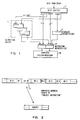
- a byte shifter 3 receives instructions from a central storage facility within the computer system and aligns the instructions during their transfer through the byte shifter.
- An instruction buffer 9 is connected to the byte shifter 3 for receiving and temporarily storing instructions from the byte shifter 3.
- An instruction register 11 is connected to the instruction buffer 9 and to the byte shifter 3 via busses 5 and 7 for receiving and storing for execution the instruction stored in the instruction buffer 9 including the special instruction, and for receiving the "subject instruction" via busses 5 and 7 from the byte shifter 3.
- An execute register 13 is interconnected between the byte shifter 3 and the instruction register 11 for temporarily storing one or more additional bytes of the instruction to be executed when the byte-length of the instruction is greater than the byte-length of the instruction register 11.
- a computer system processor 16 is connected to the instruction register 11 for receiving the instruction stored in the register 11 and for executing said instruction.
- a computer system processor 16 executes in sequence a plurality of instructions, each of the instructions being sequentially transferred to the instruction register 11 via the instruction buffer 9 for execution.
- the next instruction to be executed in the sequence is stored in the instruction buffer 9.
- the next instruction in sequence is retrieved from the instruction buffer 9, and is stored in the instruction register 11 for execution.
- the next instruction in the sequence is a special instruction, such as an EXECUTE instruction, when the special instruction is executed, another instruction, referred to herein as a "subject instruction", is retrieved from the processor's central storage facility.
- the subject instruction is not a member of the plurality of instructions sequentially executed by the computer system processor 16.
- the "subject instruction” is retrieved from the central storage facility, out-of-sequence, is transferred to the instruction register 11, and is executed by the processor 16.
- execution of the "subject instruction” is complete, a further instruction in the sequence is transferred to the instruction register 11 for execution.
- the "subject instruction" was taken out of sequence and transferred to the instruction register 11 via the instruction buffer 9.
- the previous contents of the instruction buffer 9 were destroyed.
- the previous contents of the instruction buffer 9 comprises the next instruction in the sequence to be executed following execution of the subject instruction. Since the previous contents were destroyed, re-initialization of the instruction buffer 9 was necessary - that is, the next instruction in the sequence was again retrieved from the central storage facility and was stored in the instruction buffer 9. This re-initialization consumed time and resources.
- the "subject instruction” is transferred to the instruction register 11 via paths 5 and 7, as shown in figure 1.
- Paths 5 and 7 represent a bypass path, whereby the instruction buffer 9 is bypassed during execution of the special instruction.
- the "subject instruction” is retrieved from the processor's central storage facility, in response to execution of the special instruction, it is transferred to the instruction register 11 via the bypass path, that is, paths 5 and 7, in lieu of via the instruction buffer.
- the previous contents of the instruction buffer 9, comprising the next instruction in the sequence to be executed are not lost or destroyed.
- the next instruction in the sequence, stored in the instruction buffer 9 is transferred from the buffer 9 to the instruction register 11 for execution.
- re-initialization of the instruction buffer 9 is not necessary.
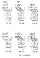
- sample instructions are illustrated. These instructions are intended to be executed in sequence and include op 0, opl, op3 through op 7, and the special instruction, namely; the EXECUTE op "Ex op".
- a "subject instruction” is also illustrated, retrieved from the processor's central storage facility in response to the execution of the EXECUTE op shown in figure 2.
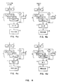
- FIG 3a through 3f a portion of a computer system of the prior art is illustrated representing various steps performed during the execution of the special EXECUTE instruction and the resultant retrieval of the "subject instruction" from the processor's central storage facility.
- the EXECUTE op is stored in the instruction register 11.
- the processor 16 executes the EXECUTE op instruction.
- the address of the "subject instruction” is calculated.
- the "subject instruction” is fetched from the central storage facility.
- the "subject instruction” is transferred to the instruction register 11 via the instruction buffer 9. Ops 3, 4, 5, and 6 were previously stored in the instruction buffer 9.
- FIG 4 a portion of a computer system of the present invention is illustrated representing various steps performed during the execution of the special EXECUTE instruction and the resultant retrieval of the "subject instruction" from the processor's central storage facility.
- the bypass path 5 and 7 of figure 1 is utilized.
- a special EXECUTE op is transferred from buffer 9 to instruction register 11 for storage and execution.
- Ops 3, 4, 5, and 6 are stored in buffer 9 and await execution in sequence.
- the EXECUTE op is stored in the instruction register 11 for execution.
- the "subject instruction" is fetched from the processor central storage facility.
- the "subject instruction” is transferred to and loaded into the instruction register 11 via byte shifter 3 and bypass paths 5 and 7 representing one feature of the present invention.
- the next instruction to be executed in sequence, op 3 is transferred from buffer 9 to the instruction register 11 for execution. Therefore, re-initialization of the instruction buffer 9 is not necessary.
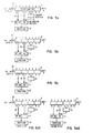
- the execute register 13 is connected between the byte shifter 3 and the instruction register 11 for receiving and storing the one or more additional bytes of the instruction to be executed. For example, if the instruction register 11 is four bytes in length, and the instruction to be executed is six bytes in length, the low-order two bytes of the instruction are stored in the execute register 13, and the high-order four bytes of the instruction are stored in the instruction register 11. The high-order four bytes are processed by the processor 16.
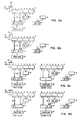
- Figure 5 illustrates a condition whereby the instruction to be executed, passing through the byte shifter 3 possesses a byte-length which is equal to or less than the byte-length of the instruction register 11. Consequently, the execute register 13 is not utilized.
- the instruction buffer 9 is not shown in the figure.
- Figure 5 also illustrates a concept. That is, the byte shifter 3 comprises a shifting or alignment apparatus for receiving the instructions from the processor's central storage facility, examining the low order bits of the instruction address representing the amount of shift required, and shifting (ie -aligning) the instruction a specified amount depending on the examined address bits of the instruction. For example, in figure 5a, the instruction address is XX---XX000. The last three low order bits of the instruction address are "000" as indicated by element no.
- dark lines 18 are shown. These lines are the bypass paths 5 and 7 of figure 1.
- the dark lines 18 indicate that one fetch is required to transfer the instruction from the central storage facility to the instruction register 11 via the byte shifter 3.
- a dark line is shown in each figure.
- a first fetch is required to transfer a portion of the instruction to the register 11 via byte shifter 3.
- a second fetch is required to transfer another portion of the instruction to the register 11 via byte shifter 3.
- the last three low order bits of the instruction address are "110" as indicated by element no. 26. As a result, both portions of the instruction are shifted from a position corresponding to byte 6 to a position corresponding to byte 0 as they pass through the byte shifter 3.
- the dark lines 18 indicate the transfer of instruction bytes.
- the dark lines 18 indicate the transfer of instruction bytes.
- since the last three bits of the instruction address are "100" as indicated by element no. 32 since the last three bits of the instruction address are "100" as indicated by element no. 32, during a first fetch of the high order bytes of the instruction, said high order bytes are shifted from a position corresponding to byte 4 to a position corresponding to byte 0 as they pass through the byte shifter 3.
- the high order bytes are stored within the instruction register 11.
- During a second fetch of the low order bytes of the instruction since the last three bits of the instruction address are "100", said low order bytes are shifted from a position corresponding to byte 4 to a position corresponding to byte 0 as they pass through the byte shifter 3.
- the low order bytes are stored within the execute register 13.
- the last three bits of the instruction address "110" indicate that the instruction is shifted from a position corresponding to byte 6 to a position corresponding to byte 0.
- a first half of the high order bytes are transferred to the instruction register 11 during a first fetch.
- a second fetch a second half of the high order bytes are transferred to the instruction register 11.
- One or more additional low order bytes of the instruction are transferred to and stored in the execute register 13. Thereafter, the one or more additional low order bytes are transferred to the instruction register 11 from the execute register 13 for execution by the processor 16.
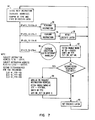
- Figure 7 illustrates an instruction processing flow chart depicting the manner by which instructions are processed utilizing the block diagram shown in figures 1 and 4 through 6 of the drawings.
- block 34 indicates that the instruction is decoded, addresses are calculated, the op-type of the instruction is determined, and the state of an execute latch is determined. The execute latch is set to "1" when the instruction being executed is an EXECUTE instruction.
- the state of the execute latch When the instruction being executed is a subject instruction of an execute instruction, the state of the execute latch will therefore be a "1". If the instruction being executed is not a subject instruction of an EXECUTE instruction, the state of the execute latch will be a "0". As indicated by block 36, if the instruction being decoded is not a subject instruction, the instruction is executed normally. If the instruction being executed is not an EXECUTE instruction and the execute latch is set to "1" (i.e. - the instruction being executed is a subject instruction of an EXECUTE instruction), the latch is reset, as indicated by block 38, and the next instruction is decoded for execution.
- the subject instruction is retrieved at address XX---XX000.
- the subject instruction passes through the byte shifter 3, it is shifted or aligned by an amount corresponding to YYY.
- the instruction register 11 is set and the execute register 13 is set, as indicated by block 42 in figure 7. If a second fetch of the target instruction is required, the second portion of the instruction is retrieved at address X'X'---X'X'000. The second portion of the instruction is shifted by an amount corresponding to YYY.
- the execute register 13 and the instruction register 11 is set, as indicated by block 44 in figure 7.
- the execute latch is set (block 46) and the next instruction (in this case, the subject instruction) is decoded. However, if a second fetch is not required, the execute latch is set (block 46) and the next instruction (in this case, the subject instruction) is decoded for execution.
- an execute exception is initiated, that is, the operation is suppressed, as indicated by block 40.
Landscapes
- Engineering & Computer Science (AREA)
- Software Systems (AREA)
- Theoretical Computer Science (AREA)
- Physics & Mathematics (AREA)
- General Engineering & Computer Science (AREA)
- General Physics & Mathematics (AREA)
- Advance Control (AREA)
- Executing Machine-Instructions (AREA)
Claims (3)
- Computersystem mit
einem Zentralspeicher zum Speichern einer Vielzahl von Befehlen und mindestens einem Sonderbefehl,
einem mit dem Zentralspeicher verbundenen Befehlspufferspeicher (9) zum sequentiellen Wiederauffinden jedes der Vielzahl von Befehlen und des Sonderbefehls im Zentralspeicher,
einem mit dem Befehlspufferspeicher verbundenen Befehlsregister (11) zum Wiederauffinden eines Befehls im Befehlspufferspeicher und zur Aufnahme mindestens einiger Bytes des Befehls während dessen Ausführung im Befehlsregister sowie
einem zwischen dem Zentralspeicher und dem Befehlsregister geschalteten Umgehungspfad (5, 7) zum Umgehen des Befehlsspeichers, so daß, wenn sich der Sonderbefehl im Befehlsregister zur Ausführung befindet, ein weiterer Befehl aus dem Zentralspeicher in das Befehlsregister über den Umgehungspfad zur Ausführung durch dasselbe übertragen wird, wodurch eine Zerstörung des Bufferspeicherinhalts vermieden wird, dadurch gekennzeichnet, daß ein Ausführungsregister (13) zwischen den Zentralspeicher und das Befehlsregister geschaltet ist zum Speichern eines oder mehrerer zusätzlicher Bytes des weiteren Befehls während dessen Übertragung vom Zentralspeicher in das Befehlsregister über den Umgehungspfad, wenn die Bytelänge des weiteren Befehls größer ist als die des Befehlsregisters. - Computersystem nach Anspruch 1, das weiterhin folgendes aufweist:
eine Byteverschiebeschaltung (3), die den Befehlspufferspeicher und das Befehlsregister mit dem Zentralspeicher verbindet, um die Bytes des vom Zentralspeicher empfangenen Befehls um einen bestimmten Wert zu verschieben, bevor einige derselben vom Befehlsregister aufgenommen und eins oder mehrere zusätzliche Bytes im Ausführungsregister gespeichert werden, wobei besagter Wert von dem Wert eines Bitsatzes abhängt, der mindestens einen Teil der Befehlsadresse umfaßt. - Computersystem nach Anspruch 2, in dem der Umgehungspfad einen Befehlsübertragungsweg umfaßt, der die Byteverschiebeschaltung mit dem Befehlsregister verbindet und den Befehlsspeicher umgeht, wobei der Befehlsübertragungsweg aktiviert wird, wenn der Sonderbefehl im Befehlsregister zur Ausführung gespeichert wird.
Applications Claiming Priority (2)
| Application Number | Priority Date | Filing Date | Title |
|---|---|---|---|
| US490813 | 1983-05-02 | ||
| US06/490,813 US4635194A (en) | 1983-05-02 | 1983-05-02 | Instruction buffer bypass apparatus |
Publications (3)
| Publication Number | Publication Date |
|---|---|
| EP0123922A2 EP0123922A2 (de) | 1984-11-07 |
| EP0123922A3 EP0123922A3 (en) | 1987-07-29 |
| EP0123922B1 true EP0123922B1 (de) | 1992-05-20 |
Family
ID=23949573
Family Applications (1)
| Application Number | Title | Priority Date | Filing Date |
|---|---|---|---|
| EP84103512A Expired EP0123922B1 (de) | 1983-05-02 | 1984-03-30 | Überbrückungsschaltung eines Befehlswortpufferspeichers |
Country Status (4)
| Country | Link |
|---|---|
| US (1) | US4635194A (de) |
| EP (1) | EP0123922B1 (de) |
| JP (1) | JPS59202544A (de) |
| DE (1) | DE3485728D1 (de) |
Families Citing this family (46)
| Publication number | Priority date | Publication date | Assignee | Title |
|---|---|---|---|---|
| JPH0630075B2 (ja) * | 1984-08-31 | 1994-04-20 | 株式会社日立製作所 | キャッシュメモリを有するデータ処理装置 |
| JPS61216032A (ja) * | 1985-02-13 | 1986-09-25 | Fujitsu Ltd | 命令バツフア回路 |
| US4860192A (en) * | 1985-02-22 | 1989-08-22 | Intergraph Corporation | Quadword boundary cache system |
| US4899275A (en) * | 1985-02-22 | 1990-02-06 | Intergraph Corporation | Cache-MMU system |
| US4933835A (en) * | 1985-02-22 | 1990-06-12 | Intergraph Corporation | Apparatus for maintaining consistency of a cache memory with a primary memory |
| US4884197A (en) * | 1985-02-22 | 1989-11-28 | Intergraph Corporation | Method and apparatus for addressing a cache memory |
| US5255384A (en) * | 1985-02-22 | 1993-10-19 | Intergraph Corporation | Memory address translation system having modifiable and non-modifiable translation mechanisms |
| JPS62117001A (ja) * | 1985-11-16 | 1987-05-28 | Hitachi Ltd | プログラマブルシ−ケンスコントロ−ラの入出力処理方法 |
| ATE49071T1 (de) * | 1986-04-23 | 1990-01-15 | Siemens Ag | Verfahren und anordnung zur beschleunigung der bereitstellung eines befehles im befehlsregister eines mikroprogrammgesteuerten prozessors. |
| US5091846A (en) * | 1986-10-03 | 1992-02-25 | Intergraph Corporation | Cache providing caching/non-caching write-through and copyback modes for virtual addresses and including bus snooping to maintain coherency |
| JPH0695305B2 (ja) * | 1986-10-22 | 1994-11-24 | 三菱電機株式会社 | デ−タ処理装置 |
| US5235686A (en) * | 1987-02-24 | 1993-08-10 | Texas Instruments Incorporated | Computer system having mixed macrocode and microcode |
| DE3750721T2 (de) * | 1987-02-24 | 1995-03-16 | Texas Instruments Inc | Computersystem mit Durchführung von vermischten Makro- und Mikrocodebefehlen. |
| US4882673A (en) * | 1987-10-02 | 1989-11-21 | Advanced Micro Devices, Inc. | Method and apparatus for testing an integrated circuit including a microprocessor and an instruction cache |
| US5313601A (en) * | 1988-01-30 | 1994-05-17 | Nec Corporation | Request control apparatus |
| JP2617974B2 (ja) * | 1988-03-08 | 1997-06-11 | 富士通株式会社 | データ処理装置 |
| JP2564624B2 (ja) * | 1988-09-20 | 1996-12-18 | 富士通株式会社 | スタック方式 |
| US4905141A (en) * | 1988-10-25 | 1990-02-27 | International Business Machines Corporation | Partitioned cache memory with partition look-aside table (PLAT) for early partition assignment identification |
| US5113515A (en) * | 1989-02-03 | 1992-05-12 | Digital Equipment Corporation | Virtual instruction cache system using length responsive decoded instruction shifting and merging with prefetch buffer outputs to fill instruction buffer |
| JP2505887B2 (ja) * | 1989-07-14 | 1996-06-12 | 富士通株式会社 | 命令処理システム |
| JP2710994B2 (ja) * | 1989-08-29 | 1998-02-10 | 三菱電機株式会社 | データ処理装置 |
| JP2695017B2 (ja) * | 1989-11-08 | 1997-12-24 | 富士通株式会社 | データ転送方式 |
| AU7305491A (en) * | 1990-01-29 | 1991-08-21 | Teraplex, Inc. | Architecture for minimal instruction set computing system |
| US5255371A (en) * | 1990-04-02 | 1993-10-19 | Unisys Corporation | Apparatus for interfacing a real-time communication link to an asynchronous digital computer system by utilizing grouped data transfer commands |
| US6378061B1 (en) * | 1990-12-20 | 2002-04-23 | Intel Corporation | Apparatus for issuing instructions and reissuing a previous instructions by recirculating using the delay circuit |
| JPH0695875A (ja) * | 1991-01-09 | 1994-04-08 | Mitsubishi Electric Corp | マイクロコンピュータのメモリアクセス方法 |
| US5655147A (en) * | 1991-02-28 | 1997-08-05 | Adaptec, Inc. | SCSI host adapter integrated circuit utilizing a sequencer circuit to control at least one non-data SCSI phase without use of any processor |
| IL100127A0 (en) * | 1991-03-11 | 1992-08-18 | Future Domain Corp | Scsi controller |
| JP2734465B2 (ja) * | 1991-04-10 | 1998-03-30 | 三菱電機株式会社 | ネットワーク用入出力装置 |
| JP3333196B2 (ja) * | 1991-07-08 | 2002-10-07 | セイコーエプソン株式会社 | トラップ処理方法 |
| US5659690A (en) * | 1992-10-15 | 1997-08-19 | Adaptec, Inc. | Programmably configurable host adapter integrated circuit including a RISC processor |
| US5463748A (en) | 1993-06-30 | 1995-10-31 | Intel Corporation | Instruction buffer for aligning instruction sets using boundary detection |
| US5604909A (en) | 1993-12-15 | 1997-02-18 | Silicon Graphics Computer Systems, Inc. | Apparatus for processing instructions in a computing system |
| JP2924643B2 (ja) * | 1994-05-19 | 1999-07-26 | ヤマハ株式会社 | ディジタル信号処理方法及び装置 |
| US5682480A (en) * | 1994-08-15 | 1997-10-28 | Hitachi, Ltd. | Parallel computer system for performing barrier synchronization by transferring the synchronization packet through a path which bypasses the packet buffer in response to an interrupt |
| US5729719A (en) * | 1994-09-07 | 1998-03-17 | Adaptec, Inc. | Synchronization circuit for clocked signals of similar frequencies |
| JP3569811B2 (ja) * | 1995-01-25 | 2004-09-29 | 株式会社ルネサステクノロジ | パイプライン処理機能を有するデータ処理装置 |
| US5754806A (en) * | 1995-11-03 | 1998-05-19 | Holtek Microelectronics, Inc. | Memory table look-up device and method |
| US5918034A (en) * | 1997-06-27 | 1999-06-29 | Sun Microsystems, Inc. | Method for decoupling pipeline stages |
| US5928355A (en) * | 1997-06-27 | 1999-07-27 | Sun Microsystems Incorporated | Apparatus for reducing instruction issue stage stalls through use of a staging register |
| JP3850156B2 (ja) | 1998-12-17 | 2006-11-29 | 富士通株式会社 | 命令処理装置 |
| US20040111594A1 (en) * | 2002-12-05 | 2004-06-10 | International Business Machines Corporation | Multithreading recycle and dispatch mechanism |
| US9361109B2 (en) | 2010-05-24 | 2016-06-07 | Qualcomm Incorporated | System and method to evaluate a data value as an instruction |
| US9354887B2 (en) * | 2010-06-28 | 2016-05-31 | International Business Machines Corporation | Instruction buffer bypass of target instruction in response to partial flush |
| JP6155723B2 (ja) * | 2013-03-18 | 2017-07-05 | 富士通株式会社 | レーダ装置及びプログラム |
| JP7373413B2 (ja) | 2020-01-21 | 2023-11-02 | 大王製紙株式会社 | シート集合包装体の製造方法 |
Family Cites Families (9)
| Publication number | Priority date | Publication date | Assignee | Title |
|---|---|---|---|---|
| FR2226079A5 (de) * | 1973-04-13 | 1974-11-08 | Honeywell Bull Soc Ind | |
| US4040031A (en) * | 1973-04-13 | 1977-08-02 | Compagnie Honeywell Bull (Societe Anonyme) | Computer instruction control apparatus and method |
| US4075686A (en) * | 1976-12-30 | 1978-02-21 | Honeywell Information Systems Inc. | Input/output cache system including bypass capability |
| US4156906A (en) * | 1977-11-22 | 1979-05-29 | Honeywell Information Systems Inc. | Buffer store including control apparatus which facilitates the concurrent processing of a plurality of commands |
| US4217640A (en) * | 1978-12-11 | 1980-08-12 | Honeywell Information Systems Inc. | Cache unit with transit block buffer apparatus |
| US4268907A (en) * | 1979-01-22 | 1981-05-19 | Honeywell Information Systems Inc. | Cache unit bypass apparatus |
| JPS5729154A (en) * | 1980-07-29 | 1982-02-17 | Fujitsu Ltd | Instruction buffer controlling system |
| JPS5843042A (ja) * | 1981-09-08 | 1983-03-12 | Fujitsu Ltd | 先行制御方式 |
| US4500954A (en) * | 1981-10-15 | 1985-02-19 | International Business Machines Corporation | Cache bypass system with post-block transfer directory examinations for updating cache and/or maintaining bypass |
-
1983
- 1983-05-02 US US06/490,813 patent/US4635194A/en not_active Expired - Fee Related
-
1984
- 1984-01-18 JP JP59005877A patent/JPS59202544A/ja active Granted
- 1984-03-30 DE DE8484103512T patent/DE3485728D1/de not_active Expired - Lifetime
- 1984-03-30 EP EP84103512A patent/EP0123922B1/de not_active Expired
Also Published As
| Publication number | Publication date |
|---|---|
| JPS6240734B2 (de) | 1987-08-29 |
| DE3485728D1 (de) | 1992-06-25 |
| US4635194A (en) | 1987-01-06 |
| EP0123922A3 (en) | 1987-07-29 |
| EP0123922A2 (de) | 1984-11-07 |
| JPS59202544A (ja) | 1984-11-16 |
Similar Documents
| Publication | Publication Date | Title |
|---|---|---|
| EP0123922B1 (de) | Überbrückungsschaltung eines Befehlswortpufferspeichers | |
| EP0071028B1 (de) | Instruktionsverarbeitungseinheit in einer Datenverarbeitungsanlage mit Instruktionssubstitution und Arbeitsverfahren | |
| US5487159A (en) | System for processing shift, mask, and merge operations in one instruction | |
| US4399507A (en) | Instruction address stack in the data memory of an instruction-pipelined processor | |
| AU619734B2 (en) | Risc computer with unaligned reference handling | |
| US4779192A (en) | Vector processor with a synchronously controlled operand fetch circuits | |
| US5996057A (en) | Data processing system and method of permutation with replication within a vector register file | |
| US4970641A (en) | Exception handling in a pipelined microprocessor | |
| US5283874A (en) | Cross coupling mechanisms for simultaneously completing consecutive pipeline instructions even if they begin to process at the same microprocessor of the issue fee | |
| US5414864A (en) | Method for selectively saving/restoring first registers and bypassing second registers in register units based on individual lock/unlock status thereof | |
| US6112288A (en) | Dynamic configurable system of parallel modules comprising chain of chips comprising parallel pipeline chain of processors with master controller feeding command and data | |
| EP0199946A2 (de) | Puffersteuerung zum Vorausholen von Befehlen und Verfahren zur Steuerung eines Befehlsvorausholpuffers | |
| EP0213842A2 (de) | Mechanismus für parallele Speicherdatenabholung und Befehlsausführung in einem Prozessor mit reduziertem Befehlssatz | |
| EP0185215A2 (de) | Mikroprozessor für Forth-ähnliche Sprache | |
| US4771380A (en) | Virtual vector registers for vector processing system | |
| EP0354585B1 (de) | Mikroprozessor mit Befehlspipeline | |
| US4792894A (en) | Arithmetic computation modifier based upon data dependent operations for SIMD architectures | |
| US4611278A (en) | Wraparound buffer for repetitive decimal numeric operations | |
| US4608633A (en) | Method for decreasing execution time of numeric instructions | |
| EP0240606B1 (de) | Verarbeitungssystem in Pipelinestruktur und Mikroprozessor mit einem derartigen System | |
| US5546551A (en) | Method and circuitry for saving and restoring status information in a pipelined computer | |
| US5812813A (en) | Apparatus and method for of register changes during execution of a micro instruction tracking sequence | |
| US5218706A (en) | Data flow processor with next destination node determination | |
| US4575795A (en) | Apparatus for detecting a predetermined character of a data string | |
| KR930003399B1 (ko) | 마이크로프로그램된 소프트웨어 명령 실행장치 및 방법 |
Legal Events
| Date | Code | Title | Description |
|---|---|---|---|
| PUAI | Public reference made under article 153(3) epc to a published international application that has entered the european phase |
Free format text: ORIGINAL CODE: 0009012 |
|
| AK | Designated contracting states |
Designated state(s): DE FR GB |
|
| 17P | Request for examination filed |
Effective date: 19841123 |
|
| PUAL | Search report despatched |
Free format text: ORIGINAL CODE: 0009013 |
|
| AK | Designated contracting states |
Kind code of ref document: A3 Designated state(s): DE FR GB |
|
| 17Q | First examination report despatched |
Effective date: 19880809 |
|
| GRAA | (expected) grant |
Free format text: ORIGINAL CODE: 0009210 |
|
| AK | Designated contracting states |
Kind code of ref document: B1 Designated state(s): DE FR GB |
|
| REF | Corresponds to: |
Ref document number: 3485728 Country of ref document: DE Date of ref document: 19920625 |
|
| ET | Fr: translation filed | ||
| PLBE | No opposition filed within time limit |
Free format text: ORIGINAL CODE: 0009261 |
|
| STAA | Information on the status of an ep patent application or granted ep patent |
Free format text: STATUS: NO OPPOSITION FILED WITHIN TIME LIMIT |
|
| PG25 | Lapsed in a contracting state [announced via postgrant information from national office to epo] |
Ref country code: GB Effective date: 19930330 |
|
| 26N | No opposition filed | ||
| GBPC | Gb: european patent ceased through non-payment of renewal fee |
Effective date: 19930330 |
|
| PG25 | Lapsed in a contracting state [announced via postgrant information from national office to epo] |
Ref country code: FR Effective date: 19931130 |
|
| PG25 | Lapsed in a contracting state [announced via postgrant information from national office to epo] |
Ref country code: DE Effective date: 19931201 |
|
| REG | Reference to a national code |
Ref country code: FR Ref legal event code: ST |