EP0116901A2 - Appareil de contrôle ultrasonore - Google Patents
Appareil de contrôle ultrasonore Download PDFInfo
- Publication number
- EP0116901A2 EP0116901A2 EP84101313A EP84101313A EP0116901A2 EP 0116901 A2 EP0116901 A2 EP 0116901A2 EP 84101313 A EP84101313 A EP 84101313A EP 84101313 A EP84101313 A EP 84101313A EP 0116901 A2 EP0116901 A2 EP 0116901A2
- Authority
- EP
- European Patent Office
- Prior art keywords
- broadband
- spectrum
- filter
- bandpass filter
- test
- Prior art date
- Legal status (The legal status is an assumption and is not a legal conclusion. Google has not performed a legal analysis and makes no representation as to the accuracy of the status listed.)
- Withdrawn
Links
Images


Classifications
-
- G—PHYSICS
- G01—MEASURING; TESTING
- G01S—RADIO DIRECTION-FINDING; RADIO NAVIGATION; DETERMINING DISTANCE OR VELOCITY BY USE OF RADIO WAVES; LOCATING OR PRESENCE-DETECTING BY USE OF THE REFLECTION OR RERADIATION OF RADIO WAVES; ANALOGOUS ARRANGEMENTS USING OTHER WAVES
- G01S15/00—Systems using the reflection or reradiation of acoustic waves, e.g. sonar systems
- G01S15/88—Sonar systems specially adapted for specific applications
- G01S15/89—Sonar systems specially adapted for specific applications for mapping or imaging
- G01S15/8906—Short-range imaging systems; Acoustic microscope systems using pulse-echo techniques
- G01S15/895—Short-range imaging systems; Acoustic microscope systems using pulse-echo techniques characterised by the transmitted frequency spectrum
- G01S15/8954—Short-range imaging systems; Acoustic microscope systems using pulse-echo techniques characterised by the transmitted frequency spectrum using a broad-band spectrum
-
- G—PHYSICS
- G01—MEASURING; TESTING
- G01N—INVESTIGATING OR ANALYSING MATERIALS BY DETERMINING THEIR CHEMICAL OR PHYSICAL PROPERTIES
- G01N29/00—Investigating or analysing materials by the use of ultrasonic, sonic or infrasonic waves; Visualisation of the interior of objects by transmitting ultrasonic or sonic waves through the object
- G01N29/34—Generating the ultrasonic, sonic or infrasonic waves, e.g. electronic circuits specially adapted therefor
- G01N29/348—Generating the ultrasonic, sonic or infrasonic waves, e.g. electronic circuits specially adapted therefor with frequency characteristics, e.g. single frequency signals, chirp signals
Definitions
- the invention relates to a device for ultrasonic testing with a shock wave transmitter, a broadband test head and a display and / or recording device for the reflected signals received by the test head.
- Ultrasonic testing is a common method for non-destructive material testing.
- the relatively unhindered and, at the high frequencies used, well-oriented propagation of ultrasound in solid bodies is used to detect defects at which sound waves are reflected. Flaws can be detected in transmission or with the help of pulse-echo technology. In the first case, the transmitted sound intensity decreases and in the second case, additional reflections between the entrance echo and the back wall echo are evaluated.
- the ultrasonic pulses are generated in that piezoelectric transducers are excited by a short, one-sided voltage surge.
- the behavior of the ultrasound impulses in the material strongly depends on the frequency or the wavelength, in particular in relation to the near field length given by the focus distance and the divergence angle in the far field, scattering and absorption as well as reflection at defects (crostack and other things) variable frequency and controllable spectral distribution "in the journal” Material edition ", 20 (1978), No. 10, pp. 372/377).
- the shock wave transmitter used in known devices for ultrasonic testing generates a one-sided negative pulse with a broadband frequency spectrum of, for example, 0 to 14 MHz.
- Such transmitters are relatively simple in construction and therefore inexpensive. However, a wide range is disadvantageous because the definition for evaluating the test data is difficult and may be impossible.
- the test frequency spectrum depends on the design and design of the test head.
- the transmitter In order to obtain a clear definition for the evaluation of the test data, it is known to design the transmitter as a narrowband transmitter, from which narrowband ultrasound pulses, preferably of variable frequency, are generated.
- This technique is known as CS (Control Signals) technique.
- the desired narrowband transmission signal is generated by modulating a monochromatic AC voltage train of the desired test frequency with a triangular or sine pulse of different exponents.
- the duration of the envelope curve must always be greater than that Period of oscillation of the test frequency to be modulated.
- the broadband test heads operated with such a narrowband transmitter generate acoustic pulses with a defined test frequency and spectral distribution.
- a narrowband transmitter requires a very high electronic circuit complexity in comparison to the usual shock wave transmitter (broadband transmitter), which in turn leads to costs that are, for example, more than 25 times the costs for a shock wave transmitter, which is part of the standard equipment of a normal ultrasonic testing device.
- the pulse spectrum is already limited in the transmitter of the transmission channel "transmitter-probe-workpiece-probe-receiver". This means that the theoretically possible bandwidth of this transmission channel is not fully used and useful information is lost, namely. those which are not present in the frequency spectrum of the transmitter, but which are possible from the other elements of the transmission channel.
- Narrow band transmitters are usually adjustable in terms of frequency and pulse width. In order to be able to carry out a test with different frequency spectra, such a narrowband transmitter must be switched from shot to shot. The test with different frequency spectra is inevitably serial with the corresponding expenditure of time.
- the object of the invention is to provide a device for ultrasound testing which works with a simple broadband shock wave transmitter and enables ultrasound tests to be carried out with a defined spectral distribution and center frequency combined with high axial and lateral resolution.
- This object is achieved according to the invention in that at least one bandpass filter is connected downstream of the test head at the reception end, which is permeable to a frequency spectrum that is considerably narrower than the broadband spectrum emitted by the transmitting crystal and that the filtered-out narrowband spectrum is connected to the display and / or recording device is.
- a tunable bandpass filter is preferably provided.
- a bypass for the broadband spectrum is expediently provided for the bandpass filter, broadband spectrum and narrowband spectrum being connected in parallel to a two-channel display and / or recording device.
- Switching means are expediently provided with which the narrowband filter is activated in selected monitor screen areas. This enables a high axial resolution to be achieved by precisely setting diaphragms.
- Another advantage is that existing ultrasonic testing systems with broadband shock wave transmitters can be easily upgraded with a bandpass filter according to the invention at low cost.
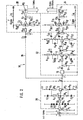
- a system is shown as it was used when performing the error tests to be described below using ultrasound.
- the ultrasound device 2 is of a known type and is only shown schematically.
- the test device is equipped with a broadband shock wave transmitter 4.
- the output 6 of the shock wave transmitter is connected to the tester head 10 via a cable 8.
- a test head with a common quartz for the transmitter and receiver was used for the tests (type H 10 MP 15 from Krautkrämer GmbH, Cologne).
- the test specimen 12 is arranged in the usual way on two supports 14 in a liquid-filled immersion pool 16 in which the test head 10 is immersed.
- the path of the transmitted pulse is dashed in the drawing and the path of the reflected pulse is shown schematically in full line.
- the cable 8 On the cable 8 is a filter system with input 1 and two outputs O 1 and O 2 connected.
- An impedance converter 20 is provided downstream of the input I.
- the signal is then switched once via a bandpass filter 22 with a downstream impedance converter 24 to the output O 1 and, secondly, via a bypass 26 with an impedance converter 28 to the output O 2 .
- the output 0 2 is connected via a cable 30 to the input 32 of the test device 2.
- the test device is provided with an oscilloscope 34, to which the transmitted pulses and the received pulses are connected.
- the transmitted pulse H On the screen of the oscilloscope 34 are the transmitted pulse H, the pulse K reflected from the surface of the workpiece, the pulse M reflected from an error W, the pulse N reflected from the back of the workpiece and that from the bottom of the plunge pool or an auxiliary reflector reflected pulse P is shown over the time base t.
- the system is also shown with a two-channel oscilloscope 36 with inputs y 1 and y 2 .
- Y 1 to the pending at 0 1 output signal and the pending at 0 2 broadband signal y 2 is connected.
- the narrowband signal F is shown above, while the broadband signal G appears below.
- a recording device 37 here schematically indicated as a tape recorder 39, can be connected with the inputs y 1 'and y 2 ' parallel to y 1 and y 2 of the oscilloscope 36.
- An analog or digital data memory 41 can also be provided for recording.
- the outputs O 1 and O 2 can also be connected to an on-line computer which can be provided instead of the recording device, but also in parallel with it.
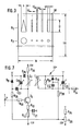
- FIG. 2 The circuit of an exemplary embodiment for the filter system 18 is shown in FIG. 2. The following short descriptions are used in the following description.
- R resistance
- C capacitor
- T transistor
- D diode
- L inductance.
- the impedance converter 20 connected downstream of the input I is constructed in two stages with the two transistors T 1 and T 2 .
- the input signal at I passes via R 2 and R 3 to the gate of transistor T 1, which is designed as a field transistor.
- the diodes D 1 to D 3 and D 4 to D 6 form an overvoltage protection against the pulses emitted by the transmitter with a voltage of approx. 300 V.
- the gate potential is set to 0 V via the resistor R 1 .
- the operating voltage of the transistors T 1 and T 2 is reduced by the Zener diodes D 7 and D 8 from the operating voltage ⁇ 15 V to 7.5 V.
- the Zener diodes 7 and 8 are connected to the operating voltage source ⁇ 15 V via the inductors L 1 , L 2 .
- the signal is divided into a broadband branch 26 and a narrowband branch 22.
- the broadband branch 26 is connected to the output 0 2 via the impedance converter 28 with an amplifier IC 1 , which is connected in a known manner.
- the impedance converter 28 is preceded by a high-pass filter (2.3 KHz) with C 3 and R 8 , which separates the DC voltage present at 0 'and suppresses the interference lying far outside the ultrasound frequency band (1-14 MHz).
- C 3 and R 8 which separates the DC voltage present at 0 'and suppresses the interference lying far outside the ultrasound frequency band (1-14 MHz).
- R 30 and R 33 and C 5 and C 6 the operating voltage for the amplifier IC 1 is sieved.
- the capacitor C 7 protects the amplifier IC 1 against destruction by DC voltages that can reach the output E2 from the outside.
- the two-stage bandpass filter 22 has a first transistor T 3 connected as a voltage-controlled current source, at the base of which the reception signal present at 0 'is connected via C 4 and R 14 .
- the bias voltage is set to 0 V via R 13 set.
- R 15 forms a strong signal coupling to avoid overloading the first stage.
- the emitter of T3 is connected to the negative voltage source - 15 V via R 15 and R 16 .
- R 16 is bridged in terms of AC voltage with C 20 and sets the quiescent current together with R 15 .
- a resonant circuit is connected to the collector, which is off. L3 and C 8 is formed. This resonant circuit has a resonance frequency of 10 MHz and is damped with R 17 .
- the signal passes via C10 and R 18 to the second filter stage with the field effect transistor T 4 , from which the source and drain are connected in the same way as the emitter and collector at T 3 .
- the resonant circuit with L 4 and C 9 is damped here by R 23 .
- R 19 and R 20 in conjunction with the capacitors C 11 and C 12 serve to decouple the operating voltage in the two filter stages.
- the output of the second filter stage is followed by the impedance converter 24, which, like the impedance converter 28 of the broadband branch, connects to the impedance matching of a 50-ohm coaxial cable. serves the output O 1 .
- the impedance converter 24 in turn has an amplifier IC 2 , which is wired in the same way as the amplifier IC 1 of the impedance converter 28.
- the output has a bandwidth of 3 dB corresponding to 400 kHz at a center frequency of the bandpass filter of 10 MHz.
- a plurality of narrowband filters can be provided in the filter system 18 parallel to one another, each of which is tuned to different frequency bands.
- These parallel narrowband filters 21, 23 are connected on the input side to the output 0 ′ of the impedance converter 20 and on the output side in each case to an impedance converter 25, 27 with outputs O 3 and O 4 .
- O 3 and 0 4 are shown in the drawing with connections to inputs y 3 and y 4 of the recording device 37 which are separate from y 1 'and y 2 ' and which are provided with separate recording tracks for the signals at y 3 and y 4 .
- an electronic switching arrangement 19, 19 'and 19 is indicated schematically at the input of the narrow-band filter (s).
- These switching arrangements can be controlled by the test device 34 via the cable 17, in such a way that the narrow-band filter in the monitor screen area of the test device.
- This enables exact setting of diaphragms, through which a high axial resolution can also be achieved in the narrowband signal, and the diaphragm can be set in such a way that only signals between surface and rear wall echo reach the narrowband filter.
- FIG. 3 shows an error standard 38 as it was used for comparison tests.
- the standard shown has a width of 30 mm and a length of 100 mm. It consists of the prepreg system CFK T300 / 914C and is designed in the form of a laminate with a total thickness of 2 mm with a layer structure (0 8 ) s .
- Local delaminations the shape of which is shown in FIG. 3, were generated as errors by a double separating film made of PTFE with a thickness of 80 ⁇ m in the central plane. In a first row B 1, these are elongated delaminations each having a length of 10 mm. Circular delaminations are arranged in a row B 2 below.
- the left delamination is designed as a triangle with a base width of 5 mm.
- the adjacent delaminations are rectangular with a width of 0.3, 0.5, 1.0 and 2.0 mm increasing to the right.
- the circular delaminations in row B 2 each have a diameter corresponding to the width of the delaminations in row B 1 .
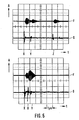
- C-scans of error standard 38 were produced and recorded with superimposed ultrasound amplitude.
- a pen-lift takes place when the amplitude drops by 6 dB with the auxiliary reflector echo and by 14 dB with the surface echo.
- the auxiliary reflector echo was generated by a glass plate which was arranged 3 mm below the sample.
- the display of the Amplitude provides further information about the course of the error margins, which should be particularly steep due to the formation of the local delaminations selected here using a double separating film.
- the edges of the delaminations become blurred, as can be seen from the illustration in FIG. 4.
- the circular delaminations with a diameter of 0.3 and 0.5 mm cannot be seen here.
- FIG. 5 A C-scan that was produced using the filter system according to the invention is shown in FIG. 5.
- the error margins are reproduced with a steep gradient in accordance with their design, and the circular errors with 0.3 and 0.5 mm diameters are also shown well resolved. Due to the steep course of the edges of all errors, the. Delaminations clearly differ from the flawless areas.
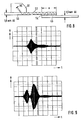
- FIG. 6 shows screen images of a two-channel oscilloscope connected in accordance with FIG. 1.
- the filtered ultrasound signal F is shown in the upper half of the screen image, while the unfiltered broadband ultrasound signal G is shown in the lower area.
- the amplitude A is shown over time t.
- FIG. 6 shows the signal image of an error-free area of the test object, while in FIG. 6 a signal image with an error display appears.
- the surface echo X and the rear side echo Y can be clearly seen in FIG. 6 above and the auxiliary reflector echo Z.
- the pulses X, Y and Z, which are recorded from the broadband received signal, can each be clearly assigned to the filtered narrowband signals.
- the error echo temporally U is clearly recognizable in the reproduction of the broadband signal between the surface echo X and the back wall echo Y.
- the auxiliary reflector echo Z is no longer recognizable.
- the high axial resolution can be seen in the lower channel, by means of which the error echo in the middle between the surface and the back wall echo can be clearly recognized and thus the error in the center of the sample can be located.
- a precise lateral determination of the error is achieved on the basis of the reproduction of the narrowband signal.
- the narrowband filter in the receiver defines the test frequency of 10 MHz with a bandwidth of 400 KHz. This enables point focusing of a few tenths of a millimeter, which results in a high lateral resolution. At the same time, the depth of the error can be measured precisely if the broadband signal, which allows a high axial resolution, is evaluated.
- a fault detection can be carried out using a plate wave test using ultrasound.
- Plate waves are generated with the help of angular test heads, through which longitudinal or transverse waves are irradiated in one of the sheets in the area of the bond.
- a test arrangement for a plate wave test is shown schematically in FIG. 8.
- two aluminum sheets 45, 46 with a thickness of 1.6 mm are arranged to overlap and are connected to one another in the overlap region a, which has a width of 20 mm, by means of an adhesive layer 54.
- the transmitting quartz 50 is arranged in the test head 51 in such a way that the sound is radiated into the upper plate at an angle ⁇ .
- the path of the sound waves in the sheet 46 is indicated by the zigzag line 52.
- test conditions can also be achieved with broadband excitation if the signals received by the test head are passed through a narrowband filter system.
- the advantage here is that existing ultrasonic testing devices can easily be retrofitted with an inexpensive filter circuit.
- a tunable filter is required for plate wave testing so that it is possible to isolate the wave mode that is optimal for the specific test conditions.
- a filter system suitable for this basically corresponds to that according to FIG. 2.
- An expedient circuit of a tunable narrowband filter 22 ′, which takes the place of the narrowband filter 22 in FIG. 1, is shown in FIG. 7.
- R 41 generates a strong negative feedback to avoid overloading.
- the band filter consisting of the coils L 7 and L 8 is with capacitance diodes D 9 , D10 tunable.
- the test frequency depends on the voltage applied to the diodes, which can be set using a R 38 spiral potentiometer.
- the other switching elements are used in a known manner to decouple DC and signal voltages.
- the filter system is designed so that the test frequency can be selected in the range from 1.0 to 2.2 MHz.
- an S / E angle test head in which the transmitting and receiving quartz are separated (2 MHz, 35 ° from Chen & Lehmann, Erftstadt) was used.
- a test frequency of 2.06 MHz was set on the narrowband filter according to FIG. 7.
- the broadband signal which is additionally evaluated for the axial resolution in the test described above with reference to FIG. 1, does not provide any useful intermediate information. Therefore, only the output of the narrowband filter 22 'was switched to the oscilloscope 36.
- Fig. 9 the amplitude A over time t shows the oscillogram of a perfect bond. Only an echo occurs here.
- a faulty connection of which the oscillogram is reproduced in FIG. 9 below, two echoes clearly appear.
- a narrow-band filter of the type described downstream of the receiver and which is tuned to an optimal wave mode With a narrow-band filter of the type described downstream of the receiver and which is tuned to an optimal wave mode, faulty adhesive connections can thus be clearly identified and reproduced. In comparison tests carried out with a broadband system of a known type, no clear differences between faulty and faultless areas could be determined.
Applications Claiming Priority (2)
| Application Number | Priority Date | Filing Date | Title |
|---|---|---|---|
| DE3304836 | 1983-02-10 | ||
| DE3304836 | 1983-02-10 |
Publications (2)
| Publication Number | Publication Date |
|---|---|
| EP0116901A2 true EP0116901A2 (fr) | 1984-08-29 |
| EP0116901A3 EP0116901A3 (fr) | 1986-06-25 |
Family
ID=6190661
Family Applications (1)
| Application Number | Title | Priority Date | Filing Date |
|---|---|---|---|
| EP84101313A Withdrawn EP0116901A3 (fr) | 1983-02-10 | 1984-02-09 | Appareil de contrôle ultrasonore |
Country Status (2)
| Country | Link |
|---|---|
| EP (1) | EP0116901A3 (fr) |
| JP (1) | JPS59193350A (fr) |
Cited By (7)
| Publication number | Priority date | Publication date | Assignee | Title |
|---|---|---|---|---|
| FR2579765A1 (fr) * | 1985-03-29 | 1986-10-03 | Labo Electronique Physique | Procede et appareil d'exploration de milieux par echographie ultrasonore |
| WO1998043110A1 (fr) * | 1997-03-21 | 1998-10-01 | Fraunhofer-Gesellschaft zur Förderung der angewandten Forschung e.V. | Dispositif d'examen par ultrasons de surfaces limites |
| US5919137A (en) * | 1996-12-04 | 1999-07-06 | Acuson Corporation | Ultrasonic diagnostic imaging system with programmable acoustic signal processor |
| US5976087A (en) * | 1996-12-04 | 1999-11-02 | Acuson Corporation | Method and apparatus for controlling acoustic signal bandwidth in an ultrasonic diagnostic imaging system |
| DE10028519A1 (de) * | 2000-06-08 | 2002-01-17 | Fraunhofer Ges Forschung | Verfahren zur Qualitätsprüfung von Bauteilen |
| EP1724925B2 (fr) † | 2005-05-13 | 2012-11-28 | Baumer Electric AG | Commutateur de proximité à ultrasons et procédé de détection d'une surface structurée à l'aide d'ondes ultrasonores |
| US20160341703A1 (en) * | 2014-01-22 | 2016-11-24 | Siemens Aktiengesellschaft | Ultrasonic test apparatus and method for ultrasonic testing |
Families Citing this family (3)
| Publication number | Priority date | Publication date | Assignee | Title |
|---|---|---|---|---|
| JPS63200058A (ja) * | 1987-02-17 | 1988-08-18 | Hitachi Constr Mach Co Ltd | 超音波探傷装置 |
| JP5456259B2 (ja) | 2008-01-30 | 2014-03-26 | 日野自動車株式会社 | 溶接検査方法および装置 |
| JP5191287B2 (ja) * | 2008-06-27 | 2013-05-08 | 日野自動車株式会社 | シーム溶接検査方法およびシーム溶接検査装置 |
Citations (6)
| Publication number | Priority date | Publication date | Assignee | Title |
|---|---|---|---|---|
| US3538753A (en) * | 1968-04-24 | 1970-11-10 | Us Army | Ultrasonic spectroscope |
| US3662589A (en) * | 1971-02-02 | 1972-05-16 | Atomic Energy Commission | Ultrasonic flaw determination by spectral analysis |
| US4016750A (en) * | 1975-11-06 | 1977-04-12 | Stanford Research Institute | Ultrasonic imaging method and apparatus |
| US4057049A (en) * | 1974-10-11 | 1977-11-08 | National Research Development Corporation | Apparatus for and methods of pulse-echo examination |
| JPS57191546A (en) * | 1981-05-21 | 1982-11-25 | Fujitsu Ltd | Ultrasonic measuring device |
| US4428237A (en) * | 1980-11-13 | 1984-01-31 | Electric Power Research Institute, Inc. | System and method for measuring ultrasonic return signals |
-
1984
- 1984-02-09 EP EP84101313A patent/EP0116901A3/fr not_active Withdrawn
- 1984-02-10 JP JP59022085A patent/JPS59193350A/ja active Pending
Patent Citations (7)
| Publication number | Priority date | Publication date | Assignee | Title |
|---|---|---|---|---|
| US3538753A (en) * | 1968-04-24 | 1970-11-10 | Us Army | Ultrasonic spectroscope |
| US3662589A (en) * | 1971-02-02 | 1972-05-16 | Atomic Energy Commission | Ultrasonic flaw determination by spectral analysis |
| US4057049A (en) * | 1974-10-11 | 1977-11-08 | National Research Development Corporation | Apparatus for and methods of pulse-echo examination |
| US4016750A (en) * | 1975-11-06 | 1977-04-12 | Stanford Research Institute | Ultrasonic imaging method and apparatus |
| US4016750B1 (en) * | 1975-11-06 | 1994-04-05 | Stanford Research Inst | Ultrasonic imaging method and apparatus |
| US4428237A (en) * | 1980-11-13 | 1984-01-31 | Electric Power Research Institute, Inc. | System and method for measuring ultrasonic return signals |
| JPS57191546A (en) * | 1981-05-21 | 1982-11-25 | Fujitsu Ltd | Ultrasonic measuring device |
Non-Patent Citations (1)
| Title |
|---|
| PATENTS ABSTRACTS OF JAPAN, Band 7, Nr. 38 (P-176) [1183], 16. Februar 1983; & JP - A - 57 191 546 (FUJITSU K.K.) 25.11.1982 * |
Cited By (11)
| Publication number | Priority date | Publication date | Assignee | Title |
|---|---|---|---|---|
| FR2579765A1 (fr) * | 1985-03-29 | 1986-10-03 | Labo Electronique Physique | Procede et appareil d'exploration de milieux par echographie ultrasonore |
| EP0197582A1 (fr) * | 1985-03-29 | 1986-10-15 | Laboratoires D'electronique Philips | Procédé et appareil d'exploration de milieux par échographie ultrasonore |
| US5919137A (en) * | 1996-12-04 | 1999-07-06 | Acuson Corporation | Ultrasonic diagnostic imaging system with programmable acoustic signal processor |
| US5976087A (en) * | 1996-12-04 | 1999-11-02 | Acuson Corporation | Method and apparatus for controlling acoustic signal bandwidth in an ultrasonic diagnostic imaging system |
| US6015385A (en) * | 1996-12-04 | 2000-01-18 | Acuson Corporation | Ultrasonic diagnostic imaging system with programmable acoustic signal processor |
| US6074347A (en) * | 1996-12-04 | 2000-06-13 | Acuson Corporation | Method and apparatus for controlling acoustic signal bandwidth in an ultrasonic diagnostic imaging system |
| WO1998043110A1 (fr) * | 1997-03-21 | 1998-10-01 | Fraunhofer-Gesellschaft zur Förderung der angewandten Forschung e.V. | Dispositif d'examen par ultrasons de surfaces limites |
| US6164136A (en) * | 1997-03-21 | 2000-12-26 | Fraunhofer-Gesellschaft Zur Forderung Der Angewandten Forschung E.V. | Device for the investigation of boundary layer areas using ultrasound |
| DE10028519A1 (de) * | 2000-06-08 | 2002-01-17 | Fraunhofer Ges Forschung | Verfahren zur Qualitätsprüfung von Bauteilen |
| EP1724925B2 (fr) † | 2005-05-13 | 2012-11-28 | Baumer Electric AG | Commutateur de proximité à ultrasons et procédé de détection d'une surface structurée à l'aide d'ondes ultrasonores |
| US20160341703A1 (en) * | 2014-01-22 | 2016-11-24 | Siemens Aktiengesellschaft | Ultrasonic test apparatus and method for ultrasonic testing |
Also Published As
| Publication number | Publication date |
|---|---|
| EP0116901A3 (fr) | 1986-06-25 |
| JPS59193350A (ja) | 1984-11-01 |
Similar Documents
| Publication | Publication Date | Title |
|---|---|---|
| DE2727691B2 (de) | Ultraschallsonde | |
| EP0336224A1 (fr) | Capteur et méthode d'examen d'émission acoustique | |
| DE2636856A1 (de) | Verfahren und vorrichtung zur zerstoerungsfreien bewertung von klebverbindungen in realzeit | |
| DE3223250A1 (de) | Verfahren und einrichtung zum identifizieren von feststoffteilchen in einer stroemung | |
| EP3418736B1 (fr) | Procédé et dispositif de mesure de bande de largeur à l'aide d'un transducteur d'ultra-sons d'air multiélémentaire | |
| EP0116901A2 (fr) | Appareil de contrôle ultrasonore | |
| DE1057356B (de) | Vorrichtung zur Materialpruefung mittels Ultraschall | |
| EP3657138B1 (fr) | Procédé de fonctionnement d'un dispositif de mesure et dispositif de mesure | |
| EP3325961A1 (fr) | Dispositif et procédé pour analyser des matériaux par spectroscopie acoustique | |
| DE2939554A1 (de) | Feuchteprofil-messanordnung mit mikrowellen | |
| DE3414362A1 (de) | Verfahren zur ultraschall-pruefung von bolzen mit einem wanddickensprung | |
| DE4414746C2 (de) | Sende-Empfangsschaltung für ein akustisches Pulsecho-Entfernungsmeßsystem | |
| DE3404492A1 (de) | Vorrichtung zur ultraschallpruefung | |
| DE2720966C2 (de) | Ultraschallsender | |
| DE1272586B (de) | Sende- und Empfangsvorrichtung fuer die Ultraschall-Werkstoffpruefung | |
| EP3444605B1 (fr) | Microphone à ultrasons pourvu de test intégré | |
| DE3221209C2 (de) | Gerät zur Untersuchung von Körpern durch Abtastung mittels Ultraschall | |
| DE102020132634A1 (de) | Ultraschallsensorsystem für ein kraftfahrzeug und verfahren zum betreiben des ultraschallsensorsystems | |
| EP0158929B1 (fr) | Procédé de contrôle ultrasonore de goujons ayant une variation de diamètre | |
| WO2020035336A1 (fr) | Dispositif de mesure pour la détermination d'une grandeur de fluide | |
| DE3835886A1 (de) | Zeitfensterautomatik fuer ultraschallmikroskop | |
| DE3217519C2 (fr) | ||
| EP0281035B1 (fr) | Procédé de surveillance pour la détermination électrodynamique de l'épaisseur et des erreurs | |
| DE2936045A1 (de) | System mit piezoelektrischem wandler und elektronischer verstaerkerschaltung fuer koerperschall-detektion | |
| DE1698149B2 (de) | Ultraschallsender zur zerstoerungsfreien werkstoffpruefung |
Legal Events
| Date | Code | Title | Description |
|---|---|---|---|
| PUAI | Public reference made under article 153(3) epc to a published international application that has entered the european phase |
Free format text: ORIGINAL CODE: 0009012 |
|
| AK | Designated contracting states |
Designated state(s): DE FR GB IT NL SE |
|
| PUAL | Search report despatched |
Free format text: ORIGINAL CODE: 0009013 |
|
| AK | Designated contracting states |
Kind code of ref document: A3 Designated state(s): DE FR GB IT NL SE |
|
| STAA | Information on the status of an ep patent application or granted ep patent |
Free format text: STATUS: THE APPLICATION IS DEEMED TO BE WITHDRAWN |
|
| 18D | Application deemed to be withdrawn |
Effective date: 19860901 |
|
| RIN1 | Information on inventor provided before grant (corrected) |
Inventor name: HILLGER, WOLFGANG, DR.-ING. |