EP0116901A2 - Apparatus for ultrasonic testing - Google Patents
Apparatus for ultrasonic testing Download PDFInfo
- Publication number
- EP0116901A2 EP0116901A2 EP84101313A EP84101313A EP0116901A2 EP 0116901 A2 EP0116901 A2 EP 0116901A2 EP 84101313 A EP84101313 A EP 84101313A EP 84101313 A EP84101313 A EP 84101313A EP 0116901 A2 EP0116901 A2 EP 0116901A2
- Authority
- EP
- European Patent Office
- Prior art keywords
- broadband
- spectrum
- filter
- bandpass filter
- test
- Prior art date
- Legal status (The legal status is an assumption and is not a legal conclusion. Google has not performed a legal analysis and makes no representation as to the accuracy of the status listed.)
- Withdrawn
Links
Images


Classifications
-
- G—PHYSICS
- G01—MEASURING; TESTING
- G01S—RADIO DIRECTION-FINDING; RADIO NAVIGATION; DETERMINING DISTANCE OR VELOCITY BY USE OF RADIO WAVES; LOCATING OR PRESENCE-DETECTING BY USE OF THE REFLECTION OR RERADIATION OF RADIO WAVES; ANALOGOUS ARRANGEMENTS USING OTHER WAVES
- G01S15/00—Systems using the reflection or reradiation of acoustic waves, e.g. sonar systems
- G01S15/88—Sonar systems specially adapted for specific applications
- G01S15/89—Sonar systems specially adapted for specific applications for mapping or imaging
- G01S15/8906—Short-range imaging systems; Acoustic microscope systems using pulse-echo techniques
- G01S15/895—Short-range imaging systems; Acoustic microscope systems using pulse-echo techniques characterised by the transmitted frequency spectrum
- G01S15/8954—Short-range imaging systems; Acoustic microscope systems using pulse-echo techniques characterised by the transmitted frequency spectrum using a broad-band spectrum
-
- G—PHYSICS
- G01—MEASURING; TESTING
- G01N—INVESTIGATING OR ANALYSING MATERIALS BY DETERMINING THEIR CHEMICAL OR PHYSICAL PROPERTIES
- G01N29/00—Investigating or analysing materials by the use of ultrasonic, sonic or infrasonic waves; Visualisation of the interior of objects by transmitting ultrasonic or sonic waves through the object
- G01N29/34—Generating the ultrasonic, sonic or infrasonic waves, e.g. electronic circuits specially adapted therefor
- G01N29/348—Generating the ultrasonic, sonic or infrasonic waves, e.g. electronic circuits specially adapted therefor with frequency characteristics, e.g. single frequency signals, chirp signals
Definitions
- the invention relates to a device for ultrasonic testing with a shock wave transmitter, a broadband test head and a display and / or recording device for the reflected signals received by the test head.
- Ultrasonic testing is a common method for non-destructive material testing.
- the relatively unhindered and, at the high frequencies used, well-oriented propagation of ultrasound in solid bodies is used to detect defects at which sound waves are reflected. Flaws can be detected in transmission or with the help of pulse-echo technology. In the first case, the transmitted sound intensity decreases and in the second case, additional reflections between the entrance echo and the back wall echo are evaluated.
- the ultrasonic pulses are generated in that piezoelectric transducers are excited by a short, one-sided voltage surge.
- the behavior of the ultrasound impulses in the material strongly depends on the frequency or the wavelength, in particular in relation to the near field length given by the focus distance and the divergence angle in the far field, scattering and absorption as well as reflection at defects (crostack and other things) variable frequency and controllable spectral distribution "in the journal” Material edition ", 20 (1978), No. 10, pp. 372/377).
- the shock wave transmitter used in known devices for ultrasonic testing generates a one-sided negative pulse with a broadband frequency spectrum of, for example, 0 to 14 MHz.
- Such transmitters are relatively simple in construction and therefore inexpensive. However, a wide range is disadvantageous because the definition for evaluating the test data is difficult and may be impossible.
- the test frequency spectrum depends on the design and design of the test head.
- the transmitter In order to obtain a clear definition for the evaluation of the test data, it is known to design the transmitter as a narrowband transmitter, from which narrowband ultrasound pulses, preferably of variable frequency, are generated.
- This technique is known as CS (Control Signals) technique.
- the desired narrowband transmission signal is generated by modulating a monochromatic AC voltage train of the desired test frequency with a triangular or sine pulse of different exponents.
- the duration of the envelope curve must always be greater than that Period of oscillation of the test frequency to be modulated.
- the broadband test heads operated with such a narrowband transmitter generate acoustic pulses with a defined test frequency and spectral distribution.
- a narrowband transmitter requires a very high electronic circuit complexity in comparison to the usual shock wave transmitter (broadband transmitter), which in turn leads to costs that are, for example, more than 25 times the costs for a shock wave transmitter, which is part of the standard equipment of a normal ultrasonic testing device.
- the pulse spectrum is already limited in the transmitter of the transmission channel "transmitter-probe-workpiece-probe-receiver". This means that the theoretically possible bandwidth of this transmission channel is not fully used and useful information is lost, namely. those which are not present in the frequency spectrum of the transmitter, but which are possible from the other elements of the transmission channel.
- Narrow band transmitters are usually adjustable in terms of frequency and pulse width. In order to be able to carry out a test with different frequency spectra, such a narrowband transmitter must be switched from shot to shot. The test with different frequency spectra is inevitably serial with the corresponding expenditure of time.
- the object of the invention is to provide a device for ultrasound testing which works with a simple broadband shock wave transmitter and enables ultrasound tests to be carried out with a defined spectral distribution and center frequency combined with high axial and lateral resolution.
- This object is achieved according to the invention in that at least one bandpass filter is connected downstream of the test head at the reception end, which is permeable to a frequency spectrum that is considerably narrower than the broadband spectrum emitted by the transmitting crystal and that the filtered-out narrowband spectrum is connected to the display and / or recording device is.
- a tunable bandpass filter is preferably provided.
- a bypass for the broadband spectrum is expediently provided for the bandpass filter, broadband spectrum and narrowband spectrum being connected in parallel to a two-channel display and / or recording device.
- Switching means are expediently provided with which the narrowband filter is activated in selected monitor screen areas. This enables a high axial resolution to be achieved by precisely setting diaphragms.
- Another advantage is that existing ultrasonic testing systems with broadband shock wave transmitters can be easily upgraded with a bandpass filter according to the invention at low cost.
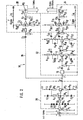
- a system is shown as it was used when performing the error tests to be described below using ultrasound.
- the ultrasound device 2 is of a known type and is only shown schematically.
- the test device is equipped with a broadband shock wave transmitter 4.
- the output 6 of the shock wave transmitter is connected to the tester head 10 via a cable 8.
- a test head with a common quartz for the transmitter and receiver was used for the tests (type H 10 MP 15 from Krautkrämer GmbH, Cologne).
- the test specimen 12 is arranged in the usual way on two supports 14 in a liquid-filled immersion pool 16 in which the test head 10 is immersed.
- the path of the transmitted pulse is dashed in the drawing and the path of the reflected pulse is shown schematically in full line.
- the cable 8 On the cable 8 is a filter system with input 1 and two outputs O 1 and O 2 connected.
- An impedance converter 20 is provided downstream of the input I.
- the signal is then switched once via a bandpass filter 22 with a downstream impedance converter 24 to the output O 1 and, secondly, via a bypass 26 with an impedance converter 28 to the output O 2 .
- the output 0 2 is connected via a cable 30 to the input 32 of the test device 2.
- the test device is provided with an oscilloscope 34, to which the transmitted pulses and the received pulses are connected.
- the transmitted pulse H On the screen of the oscilloscope 34 are the transmitted pulse H, the pulse K reflected from the surface of the workpiece, the pulse M reflected from an error W, the pulse N reflected from the back of the workpiece and that from the bottom of the plunge pool or an auxiliary reflector reflected pulse P is shown over the time base t.
- the system is also shown with a two-channel oscilloscope 36 with inputs y 1 and y 2 .
- Y 1 to the pending at 0 1 output signal and the pending at 0 2 broadband signal y 2 is connected.
- the narrowband signal F is shown above, while the broadband signal G appears below.
- a recording device 37 here schematically indicated as a tape recorder 39, can be connected with the inputs y 1 'and y 2 ' parallel to y 1 and y 2 of the oscilloscope 36.
- An analog or digital data memory 41 can also be provided for recording.
- the outputs O 1 and O 2 can also be connected to an on-line computer which can be provided instead of the recording device, but also in parallel with it.
- FIG. 2 The circuit of an exemplary embodiment for the filter system 18 is shown in FIG. 2. The following short descriptions are used in the following description.
- R resistance
- C capacitor
- T transistor
- D diode
- L inductance.
- the impedance converter 20 connected downstream of the input I is constructed in two stages with the two transistors T 1 and T 2 .
- the input signal at I passes via R 2 and R 3 to the gate of transistor T 1, which is designed as a field transistor.
- the diodes D 1 to D 3 and D 4 to D 6 form an overvoltage protection against the pulses emitted by the transmitter with a voltage of approx. 300 V.
- the gate potential is set to 0 V via the resistor R 1 .
- the operating voltage of the transistors T 1 and T 2 is reduced by the Zener diodes D 7 and D 8 from the operating voltage ⁇ 15 V to 7.5 V.
- the Zener diodes 7 and 8 are connected to the operating voltage source ⁇ 15 V via the inductors L 1 , L 2 .
- the signal is divided into a broadband branch 26 and a narrowband branch 22.
- the broadband branch 26 is connected to the output 0 2 via the impedance converter 28 with an amplifier IC 1 , which is connected in a known manner.
- the impedance converter 28 is preceded by a high-pass filter (2.3 KHz) with C 3 and R 8 , which separates the DC voltage present at 0 'and suppresses the interference lying far outside the ultrasound frequency band (1-14 MHz).
- C 3 and R 8 which separates the DC voltage present at 0 'and suppresses the interference lying far outside the ultrasound frequency band (1-14 MHz).
- R 30 and R 33 and C 5 and C 6 the operating voltage for the amplifier IC 1 is sieved.
- the capacitor C 7 protects the amplifier IC 1 against destruction by DC voltages that can reach the output E2 from the outside.
- the two-stage bandpass filter 22 has a first transistor T 3 connected as a voltage-controlled current source, at the base of which the reception signal present at 0 'is connected via C 4 and R 14 .
- the bias voltage is set to 0 V via R 13 set.
- R 15 forms a strong signal coupling to avoid overloading the first stage.
- the emitter of T3 is connected to the negative voltage source - 15 V via R 15 and R 16 .
- R 16 is bridged in terms of AC voltage with C 20 and sets the quiescent current together with R 15 .
- a resonant circuit is connected to the collector, which is off. L3 and C 8 is formed. This resonant circuit has a resonance frequency of 10 MHz and is damped with R 17 .
- the signal passes via C10 and R 18 to the second filter stage with the field effect transistor T 4 , from which the source and drain are connected in the same way as the emitter and collector at T 3 .
- the resonant circuit with L 4 and C 9 is damped here by R 23 .
- R 19 and R 20 in conjunction with the capacitors C 11 and C 12 serve to decouple the operating voltage in the two filter stages.
- the output of the second filter stage is followed by the impedance converter 24, which, like the impedance converter 28 of the broadband branch, connects to the impedance matching of a 50-ohm coaxial cable. serves the output O 1 .
- the impedance converter 24 in turn has an amplifier IC 2 , which is wired in the same way as the amplifier IC 1 of the impedance converter 28.
- the output has a bandwidth of 3 dB corresponding to 400 kHz at a center frequency of the bandpass filter of 10 MHz.
- a plurality of narrowband filters can be provided in the filter system 18 parallel to one another, each of which is tuned to different frequency bands.
- These parallel narrowband filters 21, 23 are connected on the input side to the output 0 ′ of the impedance converter 20 and on the output side in each case to an impedance converter 25, 27 with outputs O 3 and O 4 .
- O 3 and 0 4 are shown in the drawing with connections to inputs y 3 and y 4 of the recording device 37 which are separate from y 1 'and y 2 ' and which are provided with separate recording tracks for the signals at y 3 and y 4 .
- an electronic switching arrangement 19, 19 'and 19 is indicated schematically at the input of the narrow-band filter (s).
- These switching arrangements can be controlled by the test device 34 via the cable 17, in such a way that the narrow-band filter in the monitor screen area of the test device.
- This enables exact setting of diaphragms, through which a high axial resolution can also be achieved in the narrowband signal, and the diaphragm can be set in such a way that only signals between surface and rear wall echo reach the narrowband filter.
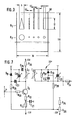
- FIG. 3 shows an error standard 38 as it was used for comparison tests.
- the standard shown has a width of 30 mm and a length of 100 mm. It consists of the prepreg system CFK T300 / 914C and is designed in the form of a laminate with a total thickness of 2 mm with a layer structure (0 8 ) s .
- Local delaminations the shape of which is shown in FIG. 3, were generated as errors by a double separating film made of PTFE with a thickness of 80 ⁇ m in the central plane. In a first row B 1, these are elongated delaminations each having a length of 10 mm. Circular delaminations are arranged in a row B 2 below.
- the left delamination is designed as a triangle with a base width of 5 mm.
- the adjacent delaminations are rectangular with a width of 0.3, 0.5, 1.0 and 2.0 mm increasing to the right.
- the circular delaminations in row B 2 each have a diameter corresponding to the width of the delaminations in row B 1 .
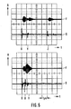
- C-scans of error standard 38 were produced and recorded with superimposed ultrasound amplitude.
- a pen-lift takes place when the amplitude drops by 6 dB with the auxiliary reflector echo and by 14 dB with the surface echo.
- the auxiliary reflector echo was generated by a glass plate which was arranged 3 mm below the sample.
- the display of the Amplitude provides further information about the course of the error margins, which should be particularly steep due to the formation of the local delaminations selected here using a double separating film.
- the edges of the delaminations become blurred, as can be seen from the illustration in FIG. 4.
- the circular delaminations with a diameter of 0.3 and 0.5 mm cannot be seen here.
- FIG. 5 A C-scan that was produced using the filter system according to the invention is shown in FIG. 5.
- the error margins are reproduced with a steep gradient in accordance with their design, and the circular errors with 0.3 and 0.5 mm diameters are also shown well resolved. Due to the steep course of the edges of all errors, the. Delaminations clearly differ from the flawless areas.
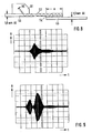
- FIG. 6 shows screen images of a two-channel oscilloscope connected in accordance with FIG. 1.
- the filtered ultrasound signal F is shown in the upper half of the screen image, while the unfiltered broadband ultrasound signal G is shown in the lower area.
- the amplitude A is shown over time t.
- FIG. 6 shows the signal image of an error-free area of the test object, while in FIG. 6 a signal image with an error display appears.
- the surface echo X and the rear side echo Y can be clearly seen in FIG. 6 above and the auxiliary reflector echo Z.
- the pulses X, Y and Z, which are recorded from the broadband received signal, can each be clearly assigned to the filtered narrowband signals.
- the error echo temporally U is clearly recognizable in the reproduction of the broadband signal between the surface echo X and the back wall echo Y.
- the auxiliary reflector echo Z is no longer recognizable.
- the high axial resolution can be seen in the lower channel, by means of which the error echo in the middle between the surface and the back wall echo can be clearly recognized and thus the error in the center of the sample can be located.
- a precise lateral determination of the error is achieved on the basis of the reproduction of the narrowband signal.
- the narrowband filter in the receiver defines the test frequency of 10 MHz with a bandwidth of 400 KHz. This enables point focusing of a few tenths of a millimeter, which results in a high lateral resolution. At the same time, the depth of the error can be measured precisely if the broadband signal, which allows a high axial resolution, is evaluated.
- a fault detection can be carried out using a plate wave test using ultrasound.
- Plate waves are generated with the help of angular test heads, through which longitudinal or transverse waves are irradiated in one of the sheets in the area of the bond.
- a test arrangement for a plate wave test is shown schematically in FIG. 8.
- two aluminum sheets 45, 46 with a thickness of 1.6 mm are arranged to overlap and are connected to one another in the overlap region a, which has a width of 20 mm, by means of an adhesive layer 54.
- the transmitting quartz 50 is arranged in the test head 51 in such a way that the sound is radiated into the upper plate at an angle ⁇ .
- the path of the sound waves in the sheet 46 is indicated by the zigzag line 52.
- test conditions can also be achieved with broadband excitation if the signals received by the test head are passed through a narrowband filter system.
- the advantage here is that existing ultrasonic testing devices can easily be retrofitted with an inexpensive filter circuit.
- a tunable filter is required for plate wave testing so that it is possible to isolate the wave mode that is optimal for the specific test conditions.
- a filter system suitable for this basically corresponds to that according to FIG. 2.
- An expedient circuit of a tunable narrowband filter 22 ′, which takes the place of the narrowband filter 22 in FIG. 1, is shown in FIG. 7.
- R 41 generates a strong negative feedback to avoid overloading.
- the band filter consisting of the coils L 7 and L 8 is with capacitance diodes D 9 , D10 tunable.
- the test frequency depends on the voltage applied to the diodes, which can be set using a R 38 spiral potentiometer.
- the other switching elements are used in a known manner to decouple DC and signal voltages.
- the filter system is designed so that the test frequency can be selected in the range from 1.0 to 2.2 MHz.
- an S / E angle test head in which the transmitting and receiving quartz are separated (2 MHz, 35 ° from Chen & Lehmann, Erftstadt) was used.
- a test frequency of 2.06 MHz was set on the narrowband filter according to FIG. 7.
- the broadband signal which is additionally evaluated for the axial resolution in the test described above with reference to FIG. 1, does not provide any useful intermediate information. Therefore, only the output of the narrowband filter 22 'was switched to the oscilloscope 36.
- Fig. 9 the amplitude A over time t shows the oscillogram of a perfect bond. Only an echo occurs here.
- a faulty connection of which the oscillogram is reproduced in FIG. 9 below, two echoes clearly appear.
- a narrow-band filter of the type described downstream of the receiver and which is tuned to an optimal wave mode With a narrow-band filter of the type described downstream of the receiver and which is tuned to an optimal wave mode, faulty adhesive connections can thus be clearly identified and reproduced. In comparison tests carried out with a broadband system of a known type, no clear differences between faulty and faultless areas could be determined.
Abstract
Description
Die Erfindung bezieht sich auf eine Vorrichtung zur Ultraschall- prüfung mit einem Stoßwellensender, einem breitbandigen Prüfkopf und einem Anzeige- und/oder Aufzeichnungsgerät für die reflektierten Signale, die vom Prüfkopf empfangen werden.The invention relates to a device for ultrasonic testing with a shock wave transmitter, a broadband test head and a display and / or recording device for the reflected signals received by the test head.
Die Ultraschallprüfung ist ein verbreitetes Verfahren zur zerstörungsfreien Werkstoffprüfung. Hierbei wird die verhältnismäßig ungehinderte und bei den verwendeten hohen Frequenzen gut ausgerichtete Ausbreitung des Ultraschalls in festen Körpern benutzt, um Fehlstellen nachzuweisen, an denen Schallwellen reflektiert werden. Fehlstellen können in Durchschallung oder mit Hilfe der Impuls-Echo-Technik nachgewiesen werden. Im ersten Fall nimmt die durchgelassene Schallintensität ab und im zweiten Fall werden zusätzliche Reflexionen zwischen dem Eintrittsecho und dem Rückwandecho ausgewertet.Ultrasonic testing is a common method for non-destructive material testing. The relatively unhindered and, at the high frequencies used, well-oriented propagation of ultrasound in solid bodies is used to detect defects at which sound waves are reflected. Flaws can be detected in transmission or with the help of pulse-echo technology. In the first case, the transmitted sound intensity decreases and in the second case, additional reflections between the entrance echo and the back wall echo are evaluated.
Bei der Ultraschallprüfung werden die Ultraschallimpulse dadurch erzeugt, daß piezoelektrische Wandler durch einen kurzen, einseitigen Spannungsstoß angeregt werden.In the ultrasonic test, the ultrasonic pulses are generated in that piezoelectric transducers are excited by a short, one-sided voltage surge.
Das Verhalten der Ultraschallimpulse im Werkstoff hängt stark von der Frequenz bzw. der Wellenlänge ab, und zwar insbesondere in bezug auf die durch den Fokusabstand gegebene Nahfeldlänge und den Divergenzwinkel im Fernfeld, Streuung und Absorption sowie Reflexion an Fehlstellen (Crostack u.a. "Ultraschallprüfung mit Sendeimpulsen stufenlos veränderlicher Frequenz und steuerbarer Spektralverteilung" in der Zeitschrift "Materialprüfung", 20 (1978), Nr. 10, S. 372/377).The behavior of the ultrasound impulses in the material strongly depends on the frequency or the wavelength, in particular in relation to the near field length given by the focus distance and the divergence angle in the far field, scattering and absorption as well as reflection at defects (crostack and other things) variable frequency and controllable spectral distribution "in the journal" Materialprüfung ", 20 (1978), No. 10, pp. 372/377).
Der in bekannten Vorrichtungen zur Ultraschallprüfung verwendete Stoßwellensender erzeugt einen einseitigen negativen Impuls mit einem breitbandigen Frequenzspektrum von beispielsweise 0 bis 14 MHz.The shock wave transmitter used in known devices for ultrasonic testing generates a one-sided negative pulse with a broadband frequency spectrum of, for example, 0 to 14 MHz.
Derartige Sender sind relativ einfach im Aufbau und daher preiswert. Eine große Bandbreite ist jedoch ungünstig, weil die Definition für die Bewertung der Prüfdaten schwierig und unter Umständen unmöglich ist. Das Prüffrequenzspektrum hängt hierbei von der Ausbildung und Auslegung des Prüfkopfes ab.Such transmitters are relatively simple in construction and therefore inexpensive. However, a wide range is disadvantageous because the definition for evaluating the test data is difficult and may be impossible. The test frequency spectrum depends on the design and design of the test head.
Um eine eindeutige Definition für die Bewertung der Prüfdaten zu erhalten, ist es bekannt, den Sender als Schmalbandsender auszubilden, von dem schmalbandige Ultraschallimpulse, vorzugsweise veränderlicher Frequenz, erzeugt werden. Diese Technik ist als CS-(Control Signals)-Technik bekannt. Hierbei wird das gewünschte schmalbandige Sendesignal durch Modulation eines monochromatischen Wechselspannungszuges der gewünschten Prüffrequenz mit einem Dreieck- oder Sinusimpuls verschiedener Exponenten erzeugt. Die Dauer der Hüllkurve muß dabei stets größer sein als die Schwingungsdauer der zu modulierenden Prüffrequenz. Die mit einem solchen Schmalbandsender betriebenen breitbandigen Prüfköpfe erzeugen akustische Impulse mit definierter Prüffrequenz und Spektralverteilung.In order to obtain a clear definition for the evaluation of the test data, it is known to design the transmitter as a narrowband transmitter, from which narrowband ultrasound pulses, preferably of variable frequency, are generated. This technique is known as CS (Control Signals) technique. The desired narrowband transmission signal is generated by modulating a monochromatic AC voltage train of the desired test frequency with a triangular or sine pulse of different exponents. The duration of the envelope curve must always be greater than that Period of oscillation of the test frequency to be modulated. The broadband test heads operated with such a narrowband transmitter generate acoustic pulses with a defined test frequency and spectral distribution.
Die Realisierung eines Schmalbandsenders erfordert einen im Vergleich zum üblichen Stoßwellensender (Breitbandsender) sehr hohen elektronischen Schaltungsäufwand, der wiederum zu Kosten führt, die beispielsweise mehr als das 25fache der Kosten für einen Stoßwellensender betragen, der zur Standardausrüstung eines normalen Ultraschallprüfgerätes gehört.The implementation of a narrowband transmitter requires a very high electronic circuit complexity in comparison to the usual shock wave transmitter (broadband transmitter), which in turn leads to costs that are, for example, more than 25 times the costs for a shock wave transmitter, which is part of the standard equipment of a normal ultrasonic testing device.
Bei der CS-Technik erfolgt die Begrenzung des Impulsspektrums bereits im Sender des übertragungskanals "Sender-Prüfkopf-Werkstück-Prüfkopf-Empfänger". Damit wird die theoretisch mögliche Bandbreite dieses übertragungskanals nicht voll ausgenutzt, und es gehen nützliche Informationen verloren, nämlich. diejenigen, die nicht im Frequenzspektrum des Senders vorhanden sind, aber von den übrigen Gliedern des übertragungskanals her möglich sind. Schmalbandsender sind normalerweise einstellbar in bezug auf Frequenz und Impulsbreite. Um eine Prüfung mit verschiedenen Frequenzspektren durchführen zu können, muß ein solcher Schmalbandsender jeweils von Schuß zu Schuß umgeschaltet werden. Die Prüfung mit unterschiedlichen Frequenzspektren ist also zwangsläufig seriell mit entsprechendem Zeitaufwand.With CS technology, the pulse spectrum is already limited in the transmitter of the transmission channel "transmitter-probe-workpiece-probe-receiver". This means that the theoretically possible bandwidth of this transmission channel is not fully used and useful information is lost, namely. those which are not present in the frequency spectrum of the transmitter, but which are possible from the other elements of the transmission channel. Narrow band transmitters are usually adjustable in terms of frequency and pulse width. In order to be able to carry out a test with different frequency spectra, such a narrowband transmitter must be switched from shot to shot. The test with different frequency spectra is inevitably serial with the corresponding expenditure of time.
Aufgabe der Erfindung ist es, eine Vorrichtung zur Ultraschall- prüfung zu schaffen, die mit einem einfachen breitbandigen Stoßwellensender arbeitet und die Durchführung von Ultraschallprüfungen mit definierter Spektralverteilung und Mittenfrequenz verbunden mit hoher axialer und lateraler Auflösung ermöglicht. Diese Aufgabe wird gemäß der Erfindung dadurch gelöst, daß dem Prüfkopf empfangsseitig wenigstens ein Bandpaßfilter nachgeschaltet ist, das für ein Frequenzspektrum durchlässig ist, das wesentlich schmaler ist als das vom Sendekristall abgegebene Breitbandspektrum und daß das ausgefilterte Schmalbandspektrum auf das Anzeige- und/oder Aufzeichnungsgerät geschaltet ist.The object of the invention is to provide a device for ultrasound testing which works with a simple broadband shock wave transmitter and enables ultrasound tests to be carried out with a defined spectral distribution and center frequency combined with high axial and lateral resolution. This object is achieved according to the invention in that at least one bandpass filter is connected downstream of the test head at the reception end, which is permeable to a frequency spectrum that is considerably narrower than the broadband spectrum emitted by the transmitting crystal and that the filtered-out narrowband spectrum is connected to the display and / or recording device is.
Vorzugsweise ist ein durchstimmbares Bandpaßfilter vorgesehen.A tunable bandpass filter is preferably provided.
Zweckmäßig ist zu dem Bandpaßfilter ein Bypass für das Breitbandspektrum vorgesehen, wobei Breitbandspektrum und Schmalbandspektrum parallel auf ein zweikanaliges Anzeige- und/oder Aufzeichnungsgerät geschaltet sind.A bypass for the broadband spectrum is expediently provided for the bandpass filter, broadband spectrum and narrowband spectrum being connected in parallel to a two-channel display and / or recording device.
Zweckmäßig sind Schaltmittel vorgesehen, mit denen in ausgewählten Monitorblendenbereichen das Schmalbandfilter wirksam gemacht wird. Hiermit kann durch exaktes Setzen von Blenden eine hohe axiale Auflösung erzielt werden.Switching means are expediently provided with which the narrowband filter is activated in selected monitor screen areas. This enables a high axial resolution to be achieved by precisely setting diaphragms.
Bei Verwendung einer Mehrzahl von parallel geschalteten Bandpaßfiltern ist eine Mehrfrequenzprüfung aus einem Schuß möglich, d.h. mit einem Ultraschallimpuls kann die Amplitude der reflektierten Ultraschallwellen unterschiedlicher Frequenzen gleichzeitig bestimmt werden.When using a plurality of bandpass filters connected in parallel, a multi-frequency test from one shot is possible, i.e. the amplitude of the reflected ultrasonic waves of different frequencies can be determined simultaneously with an ultrasonic pulse.
Soll außer einer hohen lateralen auch gleichzeitig eine hohe axiale Auflösung erreicht werden, ist bei der automatischen Auswertung für jede Monitorblende, d.h. für jeden selektierten Zeitbereich, eine separate Filterung notwendig. Das breitbandige Empfangssignal wird dazu nur im Blendenbereich auf das Empfangsfilter geschaltet. Zu diesem Zweck sind am Filtereingang Schaltmittel vorzusehen, die in Abhängigkeit von der Monitorblende geschaltet werden. Mit diesem Auswerteverfahren erreicht man selbst bei schmalbandigen und damit längeren Impulsen eine hohe axiale Auflösung.If, in addition to a high lateral resolution, a high axial resolution is to be achieved at the same time, a separate filtering is necessary for the automatic evaluation for each monitor aperture, ie for each selected time range. The broadband receive signal is only switched to the receive filter in the aperture range. For this purpose, switching means must be provided at the filter input, depending on the monitor screen be switched. With this evaluation method, high axial resolution is achieved even with narrow-band and therefore longer pulses.
Ein weiterer Vorteil besteht noch darin, daß vorhandene Ultraschallprüfanlagen mit breitbandigen Stoßwellensender mit einem Bandpaßfilter gemäß der Erfindung ohne weiteres mit geringen Kosten nachgerüstet werden können.Another advantage is that existing ultrasonic testing systems with broadband shock wave transmitters can be easily upgraded with a bandpass filter according to the invention at low cost.
Die Erfindung ist in der Zeichnung beispielsweise veranschaulicht und im nachstehenden im einzelnen anhand der Zeichnung beschrieben.
- Fig. 1 zeigt schematisch eine Ultraschallprüfanlage mit einem Bandpaßfilter gemäß der Erfindung.
- Fig. 2 zeigt die elektrische Schaltung eines Empfängerfilters mit schmalbandigem und breitbandigem Ausgang, wie er in einer Vorrichtung gemäß der Erfindung Verwendung finden kann.
- Fig. 3 zeigt ein Standard, wie. es zur Durchführung von Vergleichsversuchen verwendet wurde.
- Fig. 4 zeigt einen C-Scan mit Amplitudeneinblendungen des Standards nach Fig. 3 bei Auswertung des Breitbandsignales.
- Fig. 5 zeigt einen C-Scan mit Amplitudeneinblendung des Standard nach Fig. 3 mit Signalbehandlung durch ein empfangsseitig angeordnetes Bandpaßfilter.
- Fig. 6 zeigt zwei Oszillogramme einer fehlerfreien Stelle - Darstellung oben - und einer fehlerbehafteten Stelle - Darstellung unten -; wiedergegeben ist jeweils im oberen Signal das ausgefilterte Frequenzspektrum, während im unteren Kanal das breitbandige Frequenzspektrum erscheint.
- Fig. 7 zeigt die Schaltung eines durchstimmbaren Bandpaßfilters, wie es zur Plattenwellenprüfung verwendet wird.
- Fig. 8 zeigt das Prinzip der Plattenwellenprüfung anhand einer Blechverklebung zwischen zwei Aluminiumplatten.
- Fig. 9 zeigt die Oszillogramme einer Plattenwellenprüfung ohne Klebefehler - obere Darstellung - und mit Klebefehler - untere Darstellung.
- Fig. 1 shows schematically an ultrasonic testing system with a bandpass filter according to the invention.
- Fig. 2 shows the electrical circuit of a receiver filter with narrowband and broadband output, as it can be used in a device according to the invention.
- Fig. 3 shows a standard of how. it was used to carry out comparative tests.
- FIG. 4 shows a C-scan with amplitude overlays of the standard according to FIG. 3 when evaluating the broadband signal.
- FIG. 5 shows a C-scan with fade-in of the standard of FIG. 3 with signal treatment by a bandpass filter arranged on the receiving side.
- FIG. 6 shows two oscillograms of an error-free location - illustration above - and an error-affected location - illustration below -; the filtered frequency spectrum is shown in the upper signal, while the broadband frequency spectrum appears in the lower channel.
- Fig. 7 shows the circuit of a tunable bandpass filter as used for plate wave testing.
- Fig. 8 shows the principle of plate wave testing using a sheet metal bond between two aluminum plates.
- Fig. 9 shows the oscillograms of a plate wave test without gluing error - upper representation - and with gluing error - lower representation.
In Fig. 1 ist eine Anlage dargestellt, wie sie bei der Durchführung der weiter unten zu beschreibenden Fehlerprüfungen mittels Ultraschall verwendet wurde. Das Ultraschallgerät 2 ist von bekannter Bauart und lediglich schematisch dargestellt. Das Prüfgerät ist mit einem breitbandigen Stoßwellensender 4 ausgerüstet. Der Ausgang 6 des Stoßwellensenders ist über ein Kabel 8 mit dem Prüferkopf 10 verbunden. Für die Versuche wurde ein Prüfkopf mit einem gemeinsamen Quarz zum Sender und Empfänger verwendet (Typ H 10 MP 15 der Firma Krautkrämer GmbH, Köln). Der Prüfling 12 ist in üblicher Weise auf zwei Trägern 14 in einem mit Flüssigkeit gefüllten Tauchbecken 16 angeordnet, in dem der Prüfkopf 10 eingetaucht wird. Der Weg des gesendeten Impuls ist in der Zeichnung gestrichelt und der Weg des reflektierten Impuls in voller Linie schematisch dargestellt. An das Kabel 8 ist weiter ein Filtersystem mit dem Eingang 1 und zwei Ausgängen O1 und O2 angeschlossen. Dem Eingang I nachgeschaltet ist ein Impedanzwandler 20 vorgesehen. Das Signal wird dann einmal über ein Bandpaßfilter 22 mit nachgeschaltetem Impedanzwandler 24 auf den Ausgang O1 und zum andern über einen Bypass 26 mit einem Impedanzwandler 28 auf den Ausgang O2 geschaltet. Der Ausgang 02 steht über ein Kabel 30 mit dem Eingang 32 des Prüfgerätes 2 in Verbindung. Das Prüfgerät ist mit einem Oszilloskop 34 versehen, auf das die gesendeten Impulse und die empfangenen Impulse geschaltet sind. Auf dem Schirm des Oszilloskopen 34 sind der gesendete Impuls H, der von der Oberfläche des Werkstückes reflektierte Impuls K, der von einem Fehler W reflektierte Impuls M, der von der Rückseite des Werkstückes reflektierte Impuls N und der vom Boden des Tauchbeckens bzw. einem Hilfsreflektor reflektierte Impuls P über der Zeitbasis t dargestellt.In Fig. 1, a system is shown as it was used when performing the error tests to be described below using ultrasound. The ultrasound device 2 is of a known type and is only shown schematically. The test device is equipped with a broadband shock wave transmitter 4. The
Die Anlage ist weiter mit einem zweikanaligen Oszilloskop 36 mit den Eingängen y1 und y2 dargestellt. Auf y1 ist das bei 01 anstehende Ausgangssignal und auf y2 das bei 02 anstehende Breitbandsignal geschaltet. Das Schmalbandsignal F ist oben da.rge- stellt, während das Breitbandsignal G unten erscheint.The system is also shown with a two-
Parallel zu dem Oszilloskop kann schließlich ein Aufzeichnungsgerät 37, hier als Bandschreiber 39 schematisch angedeutet, geschaltet sein mit dem zu y1 und y2 des Oszilloskops 36 parallelen Eingängen y1' und y2'. Zur Aufzeichnung kann auch ein analoger oder digitaler Datenspeicher 41 vorgesehen werden. Die Ausgänge O1 und O2 können auch auf einen on-line betriebenen Rechner geschaltet sein, der anstatt des Aufzeichnungsgerätes, aber auch parallel zu diesem vorgesehen sein kann.Finally, parallel to the oscilloscope, a
Die Schaltung eines Ausführungsbeispieles für das Filtersystem 18 ist in Fig. 2 wiedergegeben. In der folgenden Beschreibung werden folgende Kurzbezeichnungen verwendet. R = Widerstand, C = Kondensator, T = Transistor, D = Diode und L = Induktivität.The circuit of an exemplary embodiment for the
Der dem Eingang I nachgeschaltete Impedanzwandler 20 ist zweistufig mit den beiden Transistoren T1 und T2 aufgebaut. Das Eingangssignal bei I gelangt über R2 und R3 auf das Gate des als Feldtransistor ausgebildeten Transistors T1. Die Dioden D1 bis D3 und D4 bis D6 bilden einen Überspannungschutz gegen die vom Sender mit einer Spannung von ca. 300 V abgegebenen Impulse. Über den Widerstand R1 wird das Gatepotential auf 0 V eingestellt. Die Betriebsspannung der Transistoren T1 und T2 wird mit Hilfe der Zener-Dioden D7 und D8 von der Betriebsspannung ± 15 V auf 7,5 V herabgesetzt. Die Zener-Dioden 7 und 8 sind über die Induktivitäten L1, L2 an die Betriebsspannungsquelle ± 15 V angeschaltet.The
Am Ausgang O' des Impedanzwandlers 20 wird das Signal in einen breitbandigen Zweig 26 und einen schmalbandigen Zweig 22 aufgeteilt.At the output O 'of the
Der breitbandige Zweig 26 ist über den Impedanzwandler 28 mit einem Verstärker IC1, der in bekannter Weise beschaltet ist, auf den Ausgang 02 geschaltet. Dem Impedanzwandler 28 ist ein Hochpaßfilter (2,3 KHz) mit C3 und R8 vorgeschaltet, der die an 0' anstehende Gleichspannung abtrennt und die weit außerhalb des Ultraschallfrequenzbandes (1 - 14 MHz) liegenden Störungen unterdrückt. Mit R30 und R33 sowie C5 und C6 wird die Betriebsspannung für den Verstärker IC1 gesiebt. Der Kondensator C7 schützt den Verstärker IC1 gegen Zerstörung durch Gleichspannungen, die von außen auf den Ausgang E2 gelangen können.The
Der zweistufig ausgebildete Bandpaßfilter 22 weist einen als spannungsgesteuerte Stromquelle geschalteten ersten Transistor T3 auf, an dessen Basis das bei 0' anstehende Empfangssignal über C4 und R14 angeschaltet ist. Über R13 wird die Vorspannung auf 0 V eingestellt. R15 bildet eine starke Signalkopplung, um eine Übersteuerung der ersten Stufe zu vermeiden. Der Emitter von T3 ist über R 15 und R16 mit der negativen Spannungsquelle - 15 V verbunden. R16 ist mit C20 wechselspannungsmäßig überbrückt und stellt zusammen mit R15 den Ruhestrom ein. An den Kollektor ist ein Schwingkreis angeschaltet, der aus. L3 und C8 gebildet ist. Dieser Schwingkreis hat eine Resonanzfrequenz von 10 MHz und wird mit R17 bedämpft. Das Signal gelangt über C10 und R18 auf die zweite Filterstufe mit dem Feldeffekttransistor T4, von dem Source und Drain in gleicher Weise beschaltet sind wie Emitter und Kollektor bei T3. Der Schwingkreis mit L4 und C9 ist hier durch R23 bedämpft. R19 und R20 dienen in Verbindung mit den Kondensatoren C11 und C12 der Betriebsspannungsentkopplung in den beiden Filterstufen.The two-
Dem Ausgang der zweiten Filterstufe ist der Impedanzwandler 24 nachgeschaltet, der wie der Impedanzwandler 28 des breitbandigen Zweiges zur Impedanzanpassung eines 50-Ohm-Koaxialkabels an. den Ausgang O1 dient. Der Impedanzwandler 24 weist wiederum einen Verstärker IC2 auf, der in gleicher Weise beschaltet ist wie der Verstärker IC1 des Impedanzwandlers 28. Der Ausgang hat eine Bandbreite von 3 dB entsprechend 400 kHz bei einer Mittenfrequenz des Bandpaßfilters von 10 MHz.The output of the second filter stage is followed by the
Wie in Fig. 1 dargestellt, können in dem Filtersystem 18 parallel zueinander mehrere Schmalbandfilter vorgesehen sein, die jeweils auf unterschiedliche Frequenzbänder abgestimmt sind. Diese parallelen Schmalbandfilter 21, 23 sind eingangsseitig an den Ausgang 0' des Impedanzwandlers 20 angeschlossen und ausgangsseitig jeweils an einen Impedanzwandler 25, 27 mit Ausgängen O3 und O4. O3 und 04 sind in der Zeichnung mit Verbindungen zu von y1' und y2' gesonderten Eingängen y3 und y4 des Aufzeichnungsgerätes 37 dargestellt, das für die Signale an y3 und y4 mit gesonderten Aufzeichnungsspuren versehen ist.As shown in FIG. 1, a plurality of narrowband filters can be provided in the
In Fig. 1 und 2 ist am Eingang des/der Schmalbandfilter jeweils eine elektronische Schaltanordnung 19, 19' und 19" schematisch angedeutet. Diese Schaltanordnungen sind über das Kabel 17 vom Prüfgerät 34 steuerbar, und zwar so, daß das Schmalbandfilter im Monitorblendenbereich des Prüfgerätes geschaltet wird. Auf diese Weise ist exaktes Setzen von Blenden möglich, durch die eine hohe axiale Auflösung auch im Schmalbandsignal erzielbar ist. Die Blende kann dabei so gesetzt werden, daß nur Signale zwischen Oberflächen- und Rückwandecho auf den Schmalbandfilter gelangen.1 and 2, an
In Fig. 3 ist ein Fehlerstandard 38 wiedergegeben, wie es für Vergleichsversuche verwendet worden ist. Das dargestellte Standard hat eine Breite von 30 mm und eine Länge von 100 mm. Es besteht aus dem Prepreg-System CFK T300/914C und ist in Form eines Laminats mit einer Gesamtdicke von 2 mm ausgebildet mit einem Lagenaufbau (08)s. Als Fehler wurden durch eine Doppeltrennfolie aus PTFE mit einer Dicke von 80 um in der Mittelebene lokale Delaminationen erzeugt, deren Form in Fig. 3 wiedergegeben ist. Es handelt sich hier in einer ersten Reihe B1 um länglich ausgebildete Delaminationen mit einer Länge von jeweils 10 mm. In einer Reihe B2 darunter sind kreisförmige Delaminationen angeordnet. In der Reihe B1 ist die linke Delamination als Dreieck mit einer Basisbreite von 5 mm ausgebildet. Die daneben liegenden Delaminationen sind rechteckförmig mit nach rechts steigender Breite von 0,3, 0,5, 1,0 und 2,0 mm. Die in der Reihe B2 liegenden kreisförmigen Delaminationen haben jeweils einen Durchmesser entsprechend der Breite der Delaminationen in der Reihe B1.FIG. 3 shows an error standard 38 as it was used for comparison tests. The standard shown has a width of 30 mm and a length of 100 mm. It consists of the prepreg system CFK T300 / 914C and is designed in the form of a laminate with a total thickness of 2 mm with a layer structure (0 8 ) s . Local delaminations, the shape of which is shown in FIG. 3, were generated as errors by a double separating film made of PTFE with a thickness of 80 μm in the central plane. In a first row B 1, these are elongated delaminations each having a length of 10 mm. Circular delaminations are arranged in a row B 2 below. In row B 1 , the left delamination is designed as a triangle with a base width of 5 mm. The adjacent delaminations are rectangular with a width of 0.3, 0.5, 1.0 and 2.0 mm increasing to the right. The circular delaminations in row B 2 each have a diameter corresponding to the width of the delaminations in row B 1 .
Von dem Fehlerstandard 38 wurden C-Scans hergestellt und diese mit eingeblendeter Ultraschallamplitude aufgezeichnet. Ein pen-lift erfolgt hierbei bei einem Amplitudeneinbruch um 6 dB beim Hilfsreflektorecho und um 14 dB beim Oberflächenecho. Das Hilfsreflektorecho wurde durch eine Glasplatte erzeugt, die in 3 mm Abstand unter der Probe angeordnet war. Die Einblendung der Amplitude gibt weitere Informationen über den Verlauf der Fehlerränder, der durch die hier gewählte Ausbildung der lokalen Delaminationen mit Hilfe einer Doppeltrennfolie besonders steil erfolgen sollte.C-scans of error standard 38 were produced and recorded with superimposed ultrasound amplitude. A pen-lift takes place when the amplitude drops by 6 dB with the auxiliary reflector echo and by 14 dB with the surface echo. The auxiliary reflector echo was generated by a glass plate which was arranged 3 mm below the sample. The display of the Amplitude provides further information about the course of the error margins, which should be particularly steep due to the formation of the local delaminations selected here using a double separating film.
Bei der Messung mit breitbandigem Empfangssignal werden die Ränder der Delaminationen unscharf, wie aus der Darstellung in Fig. 4 ersichtlich. Hier sind insbesondere die kreisförmigen Delaminationen mit 0,3 und 0,5 mm Durchmesser nicht zu erkennen.When measuring with a broadband received signal, the edges of the delaminations become blurred, as can be seen from the illustration in FIG. 4. In particular, the circular delaminations with a diameter of 0.3 and 0.5 mm cannot be seen here.
Ein C-Scan, der unter Verwendung des erfindungsgemäßen Filtersystems hergestellt wurde, ist in Fig. 5 dargestellt. Hier sind die Fehlerränder entsprechend ihrer Ausbildung mit steilem Verlauf wiedergegeben und auch die kreisförmigen Fehler mit 0,3 und 0,5 mm Durchmesser sind gut aufgelöst dargestellt. Durch den steilen Verlauf der Ränder aller Fehler heben sich die. Delaminationen deutlich aus den fehlerfreien Gebieten ab.A C-scan that was produced using the filter system according to the invention is shown in FIG. 5. Here, the error margins are reproduced with a steep gradient in accordance with their design, and the circular errors with 0.3 and 0.5 mm diameters are also shown well resolved. Due to the steep course of the edges of all errors, the. Delaminations clearly differ from the flawless areas.
Bei dieser hohen lateralen Auflösung wird die axiale Auflösung durch die breiteren Echos infolge der Filterung schlechter. Da am Ausgang E2 des Filtersystems 18 gleichzeitig das breitbandige Ultraschallempfangssignal zur Verfügung steht, kann dieses zur Fehlertiefenbestimmung benutzt werden. Fig. 6 zeigt Schirmbilder eines entsprechend Fig. 1 angeschlossen zweikanaligen Oszilloskops. Es-ist jeweils in der oberen Hälfte des Schirmbildes das gefilterte Ultraschallsignal F dargestellt, während im unteren Bereich das ungefilterte breitbandige Ultraschallsignal G wiedergegeben ist. Dargestellt ist die Amplitude A über der Zeit t.With this high lateral resolution, the axial resolution becomes worse due to the wider echoes due to the filtering. Since the broadband ultrasound received signal is simultaneously available at the output E2 of the
In Fig. 6 oben ist die Signalabbildung eines fehlerfreien Bereiches des Prüflings wiedergegeben, während in Fig. 6 unten eine Signalabbildung mit einer Fehleranzeige erscheint. In Fig. 6 oben ist klar erkennbar das Oberflächenecho X, das Rückseiteneeho Y und das Hilfsreflektorecho Z. Den Impulsen X, Y und Z, die aus dem breitbandigen Empfangssignal aufgezeichnet werden, können jeweils die gefilterten schmalbandigen Signale klar zugeordnet werden.6 shows the signal image of an error-free area of the test object, while in FIG. 6 a signal image with an error display appears. The surface echo X and the rear side echo Y can be clearly seen in FIG. 6 above and the auxiliary reflector echo Z. The pulses X, Y and Z, which are recorded from the broadband received signal, can each be clearly assigned to the filtered narrowband signals.
Im unteren Bild ist in der Wiedergabe des breitbandigen Signales zwischen dem Oberflächenecho X und dem Rückwandecho Y das Fehlerecho zeitlich U klar erkennbar. Das Hilfsreflektorechc Z ist nicht mehr erkennbar. Im unteren Kanal ist die hohe axiale Auflösung erkennbar, durch die das Fehlerecho in der Mitte zwischen dem Oberflächen- und dem Rückwandecho klar erkennbar und damit der Fehler in der Probenmitte lokalisierbar ist. Anhand der Wiedergabe des schmalbandigen Signales wird eine genaue laterale Bestimmung des Fehlers erreicht.In the lower picture, the error echo temporally U is clearly recognizable in the reproduction of the broadband signal between the surface echo X and the back wall echo Y. The auxiliary reflector echo Z is no longer recognizable. The high axial resolution can be seen in the lower channel, by means of which the error echo in the middle between the surface and the back wall echo can be clearly recognized and thus the error in the center of the sample can be located. A precise lateral determination of the error is achieved on the basis of the reproduction of the narrowband signal.
Hieraus ergeben sich die Vorteile des Verfahrens: das Schmalbandfilter im Empfänger definiert die Prüffrequenz von 10 MHz mit einer Bandbreite von 400 KHz. Dadurch ist eine Punkt'fokussierung von wenigen Zehntel Millimetern möglich, die eine hohe laterale Auflösung ergibt. Gleichzeitig kann die Fehlertiefe genau gemessen werden, wenn das breitbandige Signal, welches eine hohe axiale Auflösung erlaubt, ausgewertet wird.This results in the advantages of the method: the narrowband filter in the receiver defines the test frequency of 10 MHz with a bandwidth of 400 KHz. This enables point focusing of a few tenths of a millimeter, which results in a high lateral resolution. At the same time, the depth of the error can be measured precisely if the broadband signal, which allows a high axial resolution, is evaluated.
Bei Metallklebverbindungen von Blechen, wie sie beispielsweise in der Luftfahrtindustrie verwendet werden, kann eine Fehlerfeststellung durch eine Plattenwellenprüfung mittels Ultraschall durchgeführt werden. Plattenwellen werden mit Hilfe von winkelförmigen Prüfköpfen erzeugt, über die Longitudinal- oder Transversalwellen in eines der Bleche im Bereich der Verklebung eingeschallt wird. Eine Versuchsanordnung für eine Plattenwellenprüfung ist in Fig. 8 schematisch dargestellt. Hier sind zwei Aluminiumbleche 45, 46 mit einer Dicke von 1,6 mm überlappend angeordnet und im Überlappungsbereich a, der eine Breite von 20 mm hat, über eine Klebschicht 54 miteinander verbunden. Der Sendequarz 50 ist im Prüfkopf 51 so angeordnet, daß der Schall unter einem Winkel a in das obere Blech eingestrahlt wird. Der Weg der Schallwellen in dem Blech 46 ist durch die Zickzacklinie 52 angedeutet.In the case of metal sheet metal adhesive bonds, such as those used in the aerospace industry, a fault detection can be carried out using a plate wave test using ultrasound. Plate waves are generated with the help of angular test heads, through which longitudinal or transverse waves are irradiated in one of the sheets in the area of the bond. A test arrangement for a plate wave test is shown schematically in FIG. 8. Here two
Unterschiedliche Wellenmoden lassen sich durch unterschiedliche Einschallwinkel, aber auch bei konstantem Einschallwinkel durch Änderungen der Prüffrequenz erzeugen (Buch Krautkrämer, "Werkstoffprüfung mit Ultraschall", Springer-Verlag, Berlin-Göttingen-Heidelberg, 1980).Different wave modes can be generated by different insonification angles, but also at constant insonification angles by changing the test frequency (book Krautkrämer, "Material Testing with Ultrasound", Springer-Verlag, Berlin-Göttingen-Heidelberg, 1980).
Werden mehrere Wellenmoden gleichzeitig angeregt, so treten Mehrfachechos auf, die leicht als zusätzliche Fehler interpretiert werden. Um dies zu vermeiden, ist es bekannt, die Plattenwellenprüfung mit einem Schmalband-Ultraschallsender durchzuführen, wobei ein definiertes, schmalbandiges Frequenzspektrum einen einzigen Wellenmode anregt (Crostack u.a. "Ultraschallprüfung mit Sendeimpulsen stufenlos veränderlicher Frequenz und steuerbarer Spektralverteilung" in der Zeitschrift "Materialprüfung", 20 (1978), Nr. 10, S.372/377).If several wave modes are excited at the same time, multiple echoes occur, which are easily interpreted as additional errors. In order to avoid this, it is known to carry out plate wave testing with a narrowband ultrasound transmitter, with a defined, narrowband frequency spectrum stimulating a single wave mode (Crostack et al (1978), No. 10, pp.372 / 377).
In gleicher Weise wie bereits oben beschrieben, lassen sich definierte Prüfverhältnisse auch bei breitbandiger Anregung erreichen, wenn die vom Prüfkopf empfangenen Signale durch ein Schmalbandfiltersystem geleitet werden. Der Vorteil besteht auch hier darin, daß vorhandene Ultraschallprüfgeräte leicht mit einer preiswerten Filterschaltung nachgerüstet werden können.In the same way as already described above, defined test conditions can also be achieved with broadband excitation if the signals received by the test head are passed through a narrowband filter system. The advantage here is that existing ultrasonic testing devices can easily be retrofitted with an inexpensive filter circuit.
Für die Plattenwellenprüfung ist ein durchstimmbares Filter erforderlich, damit die Isolierung des für die speziellen Prüfbedingungen optimalen Wellenmodes möglich ist. Ein hierfür geeignetes Filtersystem entspricht grundsätzlich dem nach Fig. 2. Eine zweckmäßige Schaltung eines durchstimmbaren Schmalbandfilters 22', das an die Stelle des Schmalbandfilters 22 in Fig. 1 tritt, ist in Fig. 7 wiedergegeben. Das am Eingang I' anstehende Signal gelangt über R40 auf den als spannungsgesteuerte Stromquelle arbeitenden Transistor T5. R41 erzeugt eine starke Gegenkopplung, um eine übersteuerung zu vermeiden. Das aus den Spulen L7 und L8 bestehende Bandfilter ist mit Kapazitätsdioden D9, D10 durchstimmbar. Die Prüffrequenz ist abhängig von der an den Dioden anliegenden Spannung, die über einen Wendelpotentiometer R38 einstellbar ist. Die übrigen Schaltelemente dienen in bekannter Weise zur Entkopplung von Gleich- und Signalspannungen. Das Filtersystem ist hier so ausgelegt, daß die Prüffrequenz in Bereich von 1,0 bis 2,2 MHz wählbar ist. Bei der Durchführung einer Plattenwellenprüfung mit der Anordnung nach Fig. 8 wurde ein S/E Winkelprüfkopf, bei dem Sende- und Empfangsquarz getrennt sind, (2 MHz, 35° der Firma Chen & Lehmann, Erftstadt) verwendet. Am Schmalbandfilter- nach Fig. 7 war eine Prüffrequenz von 2,06 MHz eingestellt. Bei der Plattenprüfung ergibt das Breitbandsignal, das bei der oben unter Bezug auf Fig. 1 beschriebenen Prüfung für die axiale Auflösung zusätzlich ausgewertet wird, keine brauchbare Zwischeninformation. Es wurde daher nur der Ausgang des Schmalbandfilters 22' auf das Oszilloskop 36 geschaltet.A tunable filter is required for plate wave testing so that it is possible to isolate the wave mode that is optimal for the specific test conditions. A filter system suitable for this basically corresponds to that according to FIG. 2. An expedient circuit of a tunable
In Fig. 9 ist oben mit der Amplitude A über der Zeit t das Oszillogramm einer einwandfreien Klebung dargestellt. Hier tritt nur ein Echo auf. Bei einer fehlerhaften Verbindung, von der das Oszillogramm in Fig. 9 unten wiedergegeben ist, treten klar erkennbar zwei Echos auf. Mit einem dem Empfänger nachgeschalteten Schmalbandfilter der beschriebenen Art, das auf einen optimalen Wellenmode abgestimmt ist, lassen sich somit eindeutig identifizierbar und reproduzierbar fehlerhafte Klebeverbindungen feststellen. Bei Vergleichsversuchen, die mit einem Breitbandsystem bekannter Art durchgeführt werden, ließen sich keine eindeutigen Unterschiede zwischen fehlerhaften und fehlerfreien Bereichen ermitteln.In Fig. 9 the amplitude A over time t shows the oscillogram of a perfect bond. Only an echo occurs here. In the case of a faulty connection, of which the oscillogram is reproduced in FIG. 9 below, two echoes clearly appear. With a narrow-band filter of the type described downstream of the receiver and which is tuned to an optimal wave mode, faulty adhesive connections can thus be clearly identified and reproduced. In comparison tests carried out with a broadband system of a known type, no clear differences between faulty and faultless areas could be determined.
Liste der in den Schaltungen nach Fig. 2 und 7 verwendeten Bauteile


Claims (5)
Applications Claiming Priority (2)
| Application Number | Priority Date | Filing Date | Title |
|---|---|---|---|
| DE3304836 | 1983-02-10 | ||
| DE3304836 | 1983-02-10 |
Publications (2)
| Publication Number | Publication Date |
|---|---|
| EP0116901A2 true EP0116901A2 (en) | 1984-08-29 |
| EP0116901A3 EP0116901A3 (en) | 1986-06-25 |
Family
ID=6190661
Family Applications (1)
| Application Number | Title | Priority Date | Filing Date |
|---|---|---|---|
| EP84101313A Withdrawn EP0116901A3 (en) | 1983-02-10 | 1984-02-09 | Apparatus for ultrasonic testing |
Country Status (2)
| Country | Link |
|---|---|
| EP (1) | EP0116901A3 (en) |
| JP (1) | JPS59193350A (en) |
Cited By (7)
| Publication number | Priority date | Publication date | Assignee | Title |
|---|---|---|---|---|
| FR2579765A1 (en) * | 1985-03-29 | 1986-10-03 | Labo Electronique Physique | METHOD AND APPARATUS FOR MEDIUM EXPLORATION BY ULTRASONIC ULTRASONOGRAPHY |
| WO1998043110A1 (en) * | 1997-03-21 | 1998-10-01 | Fraunhofer-Gesellschaft zur Förderung der angewandten Forschung e.V. | Device for examining boundary surface areas with ultrasound |
| US5919137A (en) * | 1996-12-04 | 1999-07-06 | Acuson Corporation | Ultrasonic diagnostic imaging system with programmable acoustic signal processor |
| US5976087A (en) * | 1996-12-04 | 1999-11-02 | Acuson Corporation | Method and apparatus for controlling acoustic signal bandwidth in an ultrasonic diagnostic imaging system |
| DE10028519A1 (en) * | 2000-06-08 | 2002-01-17 | Fraunhofer Ges Forschung | Quality inspection method for cast or sintered components, involves dividing response frequency spectra into regions of fundamental resonance and above fundamental resonance depending on time |
| EP1724925B2 (en) † | 2005-05-13 | 2012-11-28 | Baumer Electric AG | Ultrasonic proximity switch and method for capturing surface structures with ultrasonic sound |
| US20160341703A1 (en) * | 2014-01-22 | 2016-11-24 | Siemens Aktiengesellschaft | Ultrasonic test apparatus and method for ultrasonic testing |
Families Citing this family (3)
| Publication number | Priority date | Publication date | Assignee | Title |
|---|---|---|---|---|
| JPS63200058A (en) * | 1987-02-17 | 1988-08-18 | Hitachi Constr Mach Co Ltd | Ultrasonic flaw detector |
| JP5456259B2 (en) * | 2008-01-30 | 2014-03-26 | 日野自動車株式会社 | Welding inspection method and apparatus |
| JP5191287B2 (en) * | 2008-06-27 | 2013-05-08 | 日野自動車株式会社 | Seam welding inspection method and seam welding inspection device |
Citations (6)
| Publication number | Priority date | Publication date | Assignee | Title |
|---|---|---|---|---|
| US3538753A (en) * | 1968-04-24 | 1970-11-10 | Us Army | Ultrasonic spectroscope |
| US3662589A (en) * | 1971-02-02 | 1972-05-16 | Atomic Energy Commission | Ultrasonic flaw determination by spectral analysis |
| US4016750A (en) * | 1975-11-06 | 1977-04-12 | Stanford Research Institute | Ultrasonic imaging method and apparatus |
| US4057049A (en) * | 1974-10-11 | 1977-11-08 | National Research Development Corporation | Apparatus for and methods of pulse-echo examination |
| JPS57191546A (en) * | 1981-05-21 | 1982-11-25 | Fujitsu Ltd | Ultrasonic measuring device |
| US4428237A (en) * | 1980-11-13 | 1984-01-31 | Electric Power Research Institute, Inc. | System and method for measuring ultrasonic return signals |
-
1984
- 1984-02-09 EP EP84101313A patent/EP0116901A3/en not_active Withdrawn
- 1984-02-10 JP JP59022085A patent/JPS59193350A/en active Pending
Patent Citations (7)
| Publication number | Priority date | Publication date | Assignee | Title |
|---|---|---|---|---|
| US3538753A (en) * | 1968-04-24 | 1970-11-10 | Us Army | Ultrasonic spectroscope |
| US3662589A (en) * | 1971-02-02 | 1972-05-16 | Atomic Energy Commission | Ultrasonic flaw determination by spectral analysis |
| US4057049A (en) * | 1974-10-11 | 1977-11-08 | National Research Development Corporation | Apparatus for and methods of pulse-echo examination |
| US4016750A (en) * | 1975-11-06 | 1977-04-12 | Stanford Research Institute | Ultrasonic imaging method and apparatus |
| US4016750B1 (en) * | 1975-11-06 | 1994-04-05 | Stanford Research Inst | Ultrasonic imaging method and apparatus |
| US4428237A (en) * | 1980-11-13 | 1984-01-31 | Electric Power Research Institute, Inc. | System and method for measuring ultrasonic return signals |
| JPS57191546A (en) * | 1981-05-21 | 1982-11-25 | Fujitsu Ltd | Ultrasonic measuring device |
Non-Patent Citations (1)
| Title |
|---|
| PATENTS ABSTRACTS OF JAPAN, Band 7, Nr. 38 (P-176) [1183], 16. Februar 1983; & JP - A - 57 191 546 (FUJITSU K.K.) 25.11.1982 * |
Cited By (11)
| Publication number | Priority date | Publication date | Assignee | Title |
|---|---|---|---|---|
| FR2579765A1 (en) * | 1985-03-29 | 1986-10-03 | Labo Electronique Physique | METHOD AND APPARATUS FOR MEDIUM EXPLORATION BY ULTRASONIC ULTRASONOGRAPHY |
| EP0197582A1 (en) * | 1985-03-29 | 1986-10-15 | Laboratoires D'electronique Philips | Method and device for the ultrasonic, echographic investigation of media |
| US5919137A (en) * | 1996-12-04 | 1999-07-06 | Acuson Corporation | Ultrasonic diagnostic imaging system with programmable acoustic signal processor |
| US5976087A (en) * | 1996-12-04 | 1999-11-02 | Acuson Corporation | Method and apparatus for controlling acoustic signal bandwidth in an ultrasonic diagnostic imaging system |
| US6015385A (en) * | 1996-12-04 | 2000-01-18 | Acuson Corporation | Ultrasonic diagnostic imaging system with programmable acoustic signal processor |
| US6074347A (en) * | 1996-12-04 | 2000-06-13 | Acuson Corporation | Method and apparatus for controlling acoustic signal bandwidth in an ultrasonic diagnostic imaging system |
| WO1998043110A1 (en) * | 1997-03-21 | 1998-10-01 | Fraunhofer-Gesellschaft zur Förderung der angewandten Forschung e.V. | Device for examining boundary surface areas with ultrasound |
| US6164136A (en) * | 1997-03-21 | 2000-12-26 | Fraunhofer-Gesellschaft Zur Forderung Der Angewandten Forschung E.V. | Device for the investigation of boundary layer areas using ultrasound |
| DE10028519A1 (en) * | 2000-06-08 | 2002-01-17 | Fraunhofer Ges Forschung | Quality inspection method for cast or sintered components, involves dividing response frequency spectra into regions of fundamental resonance and above fundamental resonance depending on time |
| EP1724925B2 (en) † | 2005-05-13 | 2012-11-28 | Baumer Electric AG | Ultrasonic proximity switch and method for capturing surface structures with ultrasonic sound |
| US20160341703A1 (en) * | 2014-01-22 | 2016-11-24 | Siemens Aktiengesellschaft | Ultrasonic test apparatus and method for ultrasonic testing |
Also Published As
| Publication number | Publication date |
|---|---|
| JPS59193350A (en) | 1984-11-01 |
| EP0116901A3 (en) | 1986-06-25 |
Similar Documents
| Publication | Publication Date | Title |
|---|---|---|
| DE2727691B2 (en) | Ultrasound probe | |
| EP0336224A1 (en) | Sensor and method for acoustic emission examination | |
| DE2636856A1 (en) | PROCESS AND DEVICE FOR NON-DESTRUCTIVE EVALUATION OF ADHESIVE CONNECTIONS IN REAL TIME | |
| DE3223250A1 (en) | METHOD AND DEVICE FOR IDENTIFYING SOLID PARTICLES IN A FLOW | |
| EP3418736B1 (en) | Method and apparatus for broadband measurement with multi- element air ultrasound sound transducers | |
| EP0116901A2 (en) | Apparatus for ultrasonic testing | |
| DE1057356B (en) | Device for material testing using ultrasound | |
| EP3657138B1 (en) | Method for operating a measuring device and measuring device | |
| WO2017012794A1 (en) | Device and method for examining materials by means of acoustic spectroscopy | |
| DE3414362A1 (en) | METHOD FOR ULTRASONIC TESTING BOLTS WITH A WALL THICKNESS | |
| DE4414746C2 (en) | Transceiver circuit for an acoustic pulse-echo distance measuring system | |
| DE3404492A1 (en) | Device for ultrasonic testing | |
| DE2720966C2 (en) | Ultrasonic transmitter | |
| DE1272586B (en) | Transmitting and receiving device for ultrasonic material testing | |
| EP3444605B1 (en) | Ultrasonic microphone with self-test | |
| DE3221209C2 (en) | Device for examining bodies by scanning them with ultrasound | |
| DE102020132634A1 (en) | ULTRASONIC SENSING SYSTEM FOR AN AUTOMOTIVE VEHICLE AND METHOD OF OPERATING THE ULTRASONIC SENSING SYSTEM | |
| EP0158929B1 (en) | Method for the ultrasonic testing of bolts with a jump in wall thickness | |
| WO2020035336A1 (en) | Measuring device for determining a fluid variable | |
| DE3835886A1 (en) | Automatic time window device for ultrasound microscope | |
| DE3217519C2 (en) | ||
| EP0281035B1 (en) | Monitoring process for the electrodynamic wall thickness and error investigation | |
| DE2936045A1 (en) | Circuitry for sound wave detectors - has filter circuits for amplifying circuit for electrodes of various widths along side of rod-shaped piezoelectric transducer | |
| DE1698149B2 (en) | ULTRASOUND TRANSMITTERS FOR NON-DESTRUCTIONAL MATERIAL TESTING | |
| DE3142069C2 (en) |
Legal Events
| Date | Code | Title | Description |
|---|---|---|---|
| PUAI | Public reference made under article 153(3) epc to a published international application that has entered the european phase |
Free format text: ORIGINAL CODE: 0009012 |
|
| AK | Designated contracting states |
Designated state(s): DE FR GB IT NL SE |
|
| PUAL | Search report despatched |
Free format text: ORIGINAL CODE: 0009013 |
|
| AK | Designated contracting states |
Kind code of ref document: A3 Designated state(s): DE FR GB IT NL SE |
|
| STAA | Information on the status of an ep patent application or granted ep patent |
Free format text: STATUS: THE APPLICATION IS DEEMED TO BE WITHDRAWN |
|
| 18D | Application deemed to be withdrawn |
Effective date: 19860901 |
|
| RIN1 | Information on inventor provided before grant (corrected) |
Inventor name: HILLGER, WOLFGANG, DR.-ING. |