EP0114920B1 - Integrated circuit resistor structure - Google Patents
Integrated circuit resistor structure Download PDFInfo
- Publication number
- EP0114920B1 EP0114920B1 EP83106489A EP83106489A EP0114920B1 EP 0114920 B1 EP0114920 B1 EP 0114920B1 EP 83106489 A EP83106489 A EP 83106489A EP 83106489 A EP83106489 A EP 83106489A EP 0114920 B1 EP0114920 B1 EP 0114920B1
- Authority
- EP
- European Patent Office
- Prior art keywords
- barrier film
- corrosion barrier
- gold
- oxide
- resistive
- Prior art date
- Legal status (The legal status is an assumption and is not a legal conclusion. Google has not performed a legal analysis and makes no representation as to the accuracy of the status listed.)
- Expired
Links
- 229910052751 metal Inorganic materials 0.000 claims description 96
- 239000002184 metal Substances 0.000 claims description 96
- 230000004888 barrier function Effects 0.000 claims description 83
- 230000007797 corrosion Effects 0.000 claims description 76
- 238000005260 corrosion Methods 0.000 claims description 76
- 239000010931 gold Substances 0.000 claims description 67
- PCHJSUWPFVWCPO-UHFFFAOYSA-N gold Chemical compound [Au] PCHJSUWPFVWCPO-UHFFFAOYSA-N 0.000 claims description 62
- 229910052737 gold Inorganic materials 0.000 claims description 62
- 239000010936 titanium Substances 0.000 claims description 53
- RTAQQCXQSZGOHL-UHFFFAOYSA-N Titanium Chemical compound [Ti] RTAQQCXQSZGOHL-UHFFFAOYSA-N 0.000 claims description 49
- 229910052719 titanium Inorganic materials 0.000 claims description 49
- 229920002120 photoresistant polymer Polymers 0.000 claims description 32
- 239000010955 niobium Substances 0.000 claims description 29
- 229910052758 niobium Inorganic materials 0.000 claims description 28
- GUCVJGMIXFAOAE-UHFFFAOYSA-N niobium atom Chemical compound [Nb] GUCVJGMIXFAOAE-UHFFFAOYSA-N 0.000 claims description 28
- 238000000034 method Methods 0.000 claims description 25
- 238000000151 deposition Methods 0.000 claims description 17
- 230000008021 deposition Effects 0.000 claims description 14
- 238000001465 metallisation Methods 0.000 claims description 14
- 230000003647 oxidation Effects 0.000 claims description 13
- 238000007254 oxidation reaction Methods 0.000 claims description 13
- ZKATWMILCYLAPD-UHFFFAOYSA-N niobium pentoxide Inorganic materials O=[Nb](=O)O[Nb](=O)=O ZKATWMILCYLAPD-UHFFFAOYSA-N 0.000 claims description 10
- 239000000758 substrate Substances 0.000 claims description 10
- 239000000155 melt Substances 0.000 claims description 3
- 150000004706 metal oxides Chemical group 0.000 claims description 2
- KDLHZDBZIXYQEI-UHFFFAOYSA-N Palladium Chemical compound [Pd] KDLHZDBZIXYQEI-UHFFFAOYSA-N 0.000 claims 2
- BASFCYQUMIYNBI-UHFFFAOYSA-N platinum Chemical compound [Pt] BASFCYQUMIYNBI-UHFFFAOYSA-N 0.000 claims 2
- ZOKXTWBITQBERF-UHFFFAOYSA-N Molybdenum Chemical compound [Mo] ZOKXTWBITQBERF-UHFFFAOYSA-N 0.000 claims 1
- KJTLSVCANCCWHF-UHFFFAOYSA-N Ruthenium Chemical compound [Ru] KJTLSVCANCCWHF-UHFFFAOYSA-N 0.000 claims 1
- QCWXUUIWCKQGHC-UHFFFAOYSA-N Zirconium Chemical compound [Zr] QCWXUUIWCKQGHC-UHFFFAOYSA-N 0.000 claims 1
- 229910052735 hafnium Inorganic materials 0.000 claims 1
- VBJZVLUMGGDVMO-UHFFFAOYSA-N hafnium atom Chemical compound [Hf] VBJZVLUMGGDVMO-UHFFFAOYSA-N 0.000 claims 1
- 229910052750 molybdenum Inorganic materials 0.000 claims 1
- 239000011733 molybdenum Substances 0.000 claims 1
- 230000001590 oxidative effect Effects 0.000 claims 1
- 229910052763 palladium Inorganic materials 0.000 claims 1
- 229910052697 platinum Inorganic materials 0.000 claims 1
- 229910052707 ruthenium Inorganic materials 0.000 claims 1
- 229910052715 tantalum Inorganic materials 0.000 claims 1
- GUVRBAGPIYLISA-UHFFFAOYSA-N tantalum atom Chemical compound [Ta] GUVRBAGPIYLISA-UHFFFAOYSA-N 0.000 claims 1
- WFKWXMTUELFFGS-UHFFFAOYSA-N tungsten Chemical compound [W] WFKWXMTUELFFGS-UHFFFAOYSA-N 0.000 claims 1
- 229910052721 tungsten Inorganic materials 0.000 claims 1
- 239000010937 tungsten Substances 0.000 claims 1
- 229910052720 vanadium Inorganic materials 0.000 claims 1
- LEONUFNNVUYDNQ-UHFFFAOYSA-N vanadium atom Chemical compound [V] LEONUFNNVUYDNQ-UHFFFAOYSA-N 0.000 claims 1
- 229910052726 zirconium Inorganic materials 0.000 claims 1
- 239000010410 layer Substances 0.000 description 55
- 238000009792 diffusion process Methods 0.000 description 16
- 229910000484 niobium oxide Inorganic materials 0.000 description 14
- URLJKFSTXLNXLG-UHFFFAOYSA-N niobium(5+);oxygen(2-) Chemical compound [O-2].[O-2].[O-2].[O-2].[O-2].[Nb+5].[Nb+5] URLJKFSTXLNXLG-UHFFFAOYSA-N 0.000 description 14
- 239000000463 material Substances 0.000 description 8
- 229910000679 solder Inorganic materials 0.000 description 8
- XKRFYHLGVUSROY-UHFFFAOYSA-N Argon Chemical compound [Ar] XKRFYHLGVUSROY-UHFFFAOYSA-N 0.000 description 6
- VYPSYNLAJGMNEJ-UHFFFAOYSA-N Silicium dioxide Chemical compound O=[Si]=O VYPSYNLAJGMNEJ-UHFFFAOYSA-N 0.000 description 6
- 238000002161 passivation Methods 0.000 description 6
- 238000005272 metallurgy Methods 0.000 description 5
- 230000006378 damage Effects 0.000 description 4
- 238000005516 engineering process Methods 0.000 description 4
- 230000001681 protective effect Effects 0.000 description 4
- 238000009966 trimming Methods 0.000 description 4
- 229910052786 argon Inorganic materials 0.000 description 3
- 239000002131 composite material Substances 0.000 description 3
- 150000002739 metals Chemical class 0.000 description 3
- 239000004065 semiconductor Substances 0.000 description 3
- 235000012239 silicon dioxide Nutrition 0.000 description 3
- 239000000377 silicon dioxide Substances 0.000 description 3
- 238000004140 cleaning Methods 0.000 description 2
- 230000005574 cross-species transmission Effects 0.000 description 2
- 230000001351 cycling effect Effects 0.000 description 2
- 238000010586 diagram Methods 0.000 description 2
- ZNKMCMOJCDFGFT-UHFFFAOYSA-N gold titanium Chemical compound [Ti].[Au] ZNKMCMOJCDFGFT-UHFFFAOYSA-N 0.000 description 2
- 239000001307 helium Substances 0.000 description 2
- 229910052734 helium Inorganic materials 0.000 description 2
- SWQJXJOGLNCZEY-UHFFFAOYSA-N helium atom Chemical compound [He] SWQJXJOGLNCZEY-UHFFFAOYSA-N 0.000 description 2
- 239000007788 liquid Substances 0.000 description 2
- 238000004519 manufacturing process Methods 0.000 description 2
- 239000002887 superconductor Substances 0.000 description 2
- 229910001258 titanium gold Inorganic materials 0.000 description 2
- 229910001020 Au alloy Inorganic materials 0.000 description 1
- 229910000846 In alloy Inorganic materials 0.000 description 1
- QVGXLLKOCUKJST-UHFFFAOYSA-N atomic oxygen Chemical compound [O] QVGXLLKOCUKJST-UHFFFAOYSA-N 0.000 description 1
- 238000012512 characterization method Methods 0.000 description 1
- 239000004020 conductor Substances 0.000 description 1
- 230000003247 decreasing effect Effects 0.000 description 1
- 230000007547 defect Effects 0.000 description 1
- 230000001066 destructive effect Effects 0.000 description 1
- 230000003628 erosive effect Effects 0.000 description 1
- 230000005284 excitation Effects 0.000 description 1
- 150000002343 gold Chemical class 0.000 description 1
- 239000003353 gold alloy Substances 0.000 description 1
- 238000010348 incorporation Methods 0.000 description 1
- 229910044991 metal oxide Inorganic materials 0.000 description 1
- 239000000615 nonconductor Substances 0.000 description 1
- 239000001301 oxygen Substances 0.000 description 1
- 229910052760 oxygen Inorganic materials 0.000 description 1
- JRTYPQGPARWINR-UHFFFAOYSA-N palladium platinum Chemical compound [Pd].[Pt] JRTYPQGPARWINR-UHFFFAOYSA-N 0.000 description 1
- 230000002265 prevention Effects 0.000 description 1
- 239000002344 surface layer Substances 0.000 description 1
- MZLGASXMSKOWSE-UHFFFAOYSA-N tantalum nitride Chemical compound [Ta]#N MZLGASXMSKOWSE-UHFFFAOYSA-N 0.000 description 1
- 150000003608 titanium Chemical class 0.000 description 1
Images
Classifications
-
- H—ELECTRICITY
- H10—SEMICONDUCTOR DEVICES; ELECTRIC SOLID-STATE DEVICES NOT OTHERWISE PROVIDED FOR
- H10N—ELECTRIC SOLID-STATE DEVICES NOT OTHERWISE PROVIDED FOR
- H10N60/00—Superconducting devices
- H10N60/01—Manufacture or treatment
- H10N60/0156—Manufacture or treatment of devices comprising Nb or an alloy of Nb with one or more of the elements of group IVB, e.g. titanium, zirconium or hafnium
-
- H—ELECTRICITY
- H10—SEMICONDUCTOR DEVICES; ELECTRIC SOLID-STATE DEVICES NOT OTHERWISE PROVIDED FOR
- H10N—ELECTRIC SOLID-STATE DEVICES NOT OTHERWISE PROVIDED FOR
- H10N69/00—Integrated devices, or assemblies of multiple devices, comprising at least one superconducting element covered by group H10N60/00
-
- Y—GENERAL TAGGING OF NEW TECHNOLOGICAL DEVELOPMENTS; GENERAL TAGGING OF CROSS-SECTIONAL TECHNOLOGIES SPANNING OVER SEVERAL SECTIONS OF THE IPC; TECHNICAL SUBJECTS COVERED BY FORMER USPC CROSS-REFERENCE ART COLLECTIONS [XRACs] AND DIGESTS
- Y10—TECHNICAL SUBJECTS COVERED BY FORMER USPC
- Y10S—TECHNICAL SUBJECTS COVERED BY FORMER USPC CROSS-REFERENCE ART COLLECTIONS [XRACs] AND DIGESTS
- Y10S505/00—Superconductor technology: apparatus, material, process
- Y10S505/80—Material per se process of making same
- Y10S505/812—Stock
- Y10S505/813—Wire, tape, or film
-
- Y—GENERAL TAGGING OF NEW TECHNOLOGICAL DEVELOPMENTS; GENERAL TAGGING OF CROSS-SECTIONAL TECHNOLOGIES SPANNING OVER SEVERAL SECTIONS OF THE IPC; TECHNICAL SUBJECTS COVERED BY FORMER USPC CROSS-REFERENCE ART COLLECTIONS [XRACs] AND DIGESTS
- Y10—TECHNICAL SUBJECTS COVERED BY FORMER USPC
- Y10T—TECHNICAL SUBJECTS COVERED BY FORMER US CLASSIFICATION
- Y10T428/00—Stock material or miscellaneous articles
- Y10T428/12—All metal or with adjacent metals
- Y10T428/12493—Composite; i.e., plural, adjacent, spatially distinct metal components [e.g., layers, joint, etc.]
- Y10T428/12528—Semiconductor component
-
- Y—GENERAL TAGGING OF NEW TECHNOLOGICAL DEVELOPMENTS; GENERAL TAGGING OF CROSS-SECTIONAL TECHNOLOGIES SPANNING OVER SEVERAL SECTIONS OF THE IPC; TECHNICAL SUBJECTS COVERED BY FORMER USPC CROSS-REFERENCE ART COLLECTIONS [XRACs] AND DIGESTS
- Y10—TECHNICAL SUBJECTS COVERED BY FORMER USPC
- Y10T—TECHNICAL SUBJECTS COVERED BY FORMER US CLASSIFICATION
- Y10T428/00—Stock material or miscellaneous articles
- Y10T428/12—All metal or with adjacent metals
- Y10T428/12493—Composite; i.e., plural, adjacent, spatially distinct metal components [e.g., layers, joint, etc.]
- Y10T428/12771—Transition metal-base component
- Y10T428/12806—Refractory [Group IVB, VB, or VIB] metal-base component
- Y10T428/12819—Group VB metal-base component
-
- Y—GENERAL TAGGING OF NEW TECHNOLOGICAL DEVELOPMENTS; GENERAL TAGGING OF CROSS-SECTIONAL TECHNOLOGIES SPANNING OVER SEVERAL SECTIONS OF THE IPC; TECHNICAL SUBJECTS COVERED BY FORMER USPC CROSS-REFERENCE ART COLLECTIONS [XRACs] AND DIGESTS
- Y10—TECHNICAL SUBJECTS COVERED BY FORMER USPC
- Y10T—TECHNICAL SUBJECTS COVERED BY FORMER US CLASSIFICATION
- Y10T428/00—Stock material or miscellaneous articles
- Y10T428/12—All metal or with adjacent metals
- Y10T428/12493—Composite; i.e., plural, adjacent, spatially distinct metal components [e.g., layers, joint, etc.]
- Y10T428/12771—Transition metal-base component
- Y10T428/12861—Group VIII or IB metal-base component
- Y10T428/12889—Au-base component
Definitions
- This invention relates to an integrated circuit resistor structure for resistively connecting intrinsically oxidizable conductive metal layers arranged on a non-conducting substrate and to a method of preparing such a resistor structure.
- Simple metal resistors of a metal such as titanium have many desirable features such as mechanical strength, thermal stability and easy control of resistance values, but are susceptible to corrosion when in contact with niobium films.
- gold has desirable anticorrosive barrier properties and that gold is a good conductor suitable for use as a metallization region.
- Certain gold alloys and gold layers have been used and suggested in a number of anticorrosive contact characterizations. Gold, however, is not a good diffusion barrier.
- niobium is a useful superconductor, susceptible to passivation by oxidation, which is capable both in metallic form and oxide form of withstanding temperature cycling between room temperature and- liquid helium temperature.
- Niobium is known to grow an intrinsic oxide, a surface layer of Nb 2 0 5 which forms naturally at ambient temperatures in ambient atmospheres containing oxygen.
- U.S. Patent 3,907,620, Abraham et al "A Process of Forming Metallization Structures on Semiconductor Devices", shows a process for forming tantalum nitride layers on a semiconductor. Abraham et al does not, however, show any technique for passivating a ring around a barrier film to prevent corrosive intimate contact between incompatible materials.
- One object of the invention is to provide a self-aligned resistive contact structure for cryogenic temperature applications, which resistive contact structure is minimally subject to destruction by corrosion and to destruction by diffusion.
- Another object of the invention is to provide a resistor contact structure for cryogenic applications, which resistor structure is capable of withstanding the stresses of repeated heat cycling from room temperature to cryogenic temperatures, is easily fabricated, and does not suffer early life failures due to corrosive contact between electrochemically non-compatible materials nor to early life failures due to diffusion of unwanted atoms from adjacent layers in composite structures.
- Another object of the invention is to provide, in a contact structure of a plurality of layers of corrosively contrasting materials, a passivation ring encircled barrier contact which permit conduction without permitting corrosive contact of incompatible layers.
- Another object is to provide a superconductive integrated circuit technology with a trimmable resistor structure.
- Another object of a particular embodiment of the invention is to provide a multi-focus technique for successive depositions of mutually protective metals and passivation layers, taking advantage of overhang of the surface opening in a photoresist and differently focused successive depositions so as to ensure very close overlaps of the successively deposited materials.
- the invention as claimed is intended to meet these objectives and to, thereby, remedy the drawbacks of hitherto known structures and methods.
- the advantages offered by the invention are mainly that a resistor structure is now provided which is particularly useful for superconductive materials operated at cryogenic temperatures and applicable in integrated circuit technology, and that prevents erosion and diffusion problems otherwise encountered with non-compatible materials used for the conductive lines and for the resistive connections, respectively.
- the invention concerns a minimal corrosion resistor metallurgy and deposition technique especially well suited to very low temperatures associated with superconductors.
- the invention operates by extrinsic metal oxide passivating the oxidizable conductive metal perimeter ring around a barrier film contact area, by for instance, a plasma oxidation, permitting a subsequent resistive metal layer to make good resistive metal/ corrosion barrier film/conductive metal contact without the corrosion susceptibility of resistive metal/conductive metal intimate contact.
- the oxidizable conductive metal used as a base electrode must have contact areas cleaned of the intrinsic oxide layer for contacting integrated resistive metal resistors. These areas are defined by openings in photoresist; the photoresist development process leaves a photoresist overhang. The actual area of exposed oxidizable conductive metal after cleaning is greater by the amount of the overhand than is the opening in the surface of the photoresist.
- a thin corrosion barrier metal film is deposited, through the opening in the photoresist, onto the cleaned oxidizable conductive metal.
- the resistive metal is deposited over the corrosion barrier film.
- the corrosion barrier film lies between the resistive metal layer and the conductive (includes superconductive) metal layer to prevent the resistive metal from making intimate contact with the conductive metal.
- the contact area is coated with the corrosion barrier film layer only in the central area of the oxide-free cleaned area of the oxidizable conductive metal layer, as defined by the opening in the surface of the photoresist; the resistive metal layer is deposited over the corrosion barrier film, defined by the same opening in the surface of the photoresist.
- an unfocused plasma oxidation step is introduced after the corrosion barrier film deposition but before the resistive metal deposition.
- This plasma oxidation step causes oxidation of the bare oxidizable conductive metal ring exposed underneath the photoresist overhang, forming an oxide passivating ring around the corrosion barrier contact area.
- This passivating ring eliminates the possibility of any intimate contact between oxidizable conductive metal and the resistive metal.
- the corrosion barrier film does not oxidize readily; this oxidation step converts the exposed oxidizable conductive metal to its passivating oxide without harming the surface of the corrosion barrier film, which remains conductive and receptive to further deposition of resistive metal.
- the resistive metal layer is deposited from a melt larger than the melt used to deposit the corrosion barrier metal, which focuses the resistive metal deposition over a greater area to cover the edges of the corrosion barrier metal - and thus to form a resistive metal diffusion barrier over the entire corrosion barrier metal film, making possible further metallizations, such as contact by low temperature solder, without danger of destructive diffusion.
- the corrosion barrier metal film protects the resistive metal from destruction by corrosion; the resistive metal layer protects the corrosion barrier metal from destruction by diffusion.
- the passivating ring seals the edges.
- a preferred resistive metal is titanium; a preferred corrosion barrier metal is gold; a preferred conductive metal (superconductive metal) is niobium.
- the gold/titanium resistor is made compatible with lead-gold-indium alloys by making use of a titanium melt larger in size than the gold melt.
- the titanium atoms from the larger area melt are not so sharply focused and deposit farther under the photoresist overhang than do the more sharply focused gold atoms, the titanium metal thus overlapping the edge of the gold film onto the niobium oxide passivating ring. This overlap eliminates any possibility of intimate contact between the gold underneath the titanium and the lead-gold-indium metallurgy added above the titanium.
- lead-gold-indium metallurgy is useful in trimming resistors by providing appropriate superconductive shunts over selected portions along the length of the respective resistors.
- the end results of the technique of the preferred embodiment is a resistor contacting two niobium metal areas of a printed circuit.
- the niobium metal areas may be, for example, areas of a base electrode in a Josephson junction technology integrated circuit.
- the resistor may be trimmed from high to low by an applied shunt of superconductive solder.
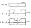
- FIG. 1 illustrates in FIGS. 1.1.-1.7 the major steps required to carry out the invention.
- FIG. 1.1 shows a niobium metal layer 11 with its surface covered by intrinsic niobium oxide layer 12.
- the intrinsic niobium oxide layer is Nb 2 0 5 and grows normally at room temperature in air.
- the intrinsic niobium oxide layer passivates the niobium metal layer and may, in many situations, be considered advantageous.
- the intrinsic niobium oxide layer has relatively higher resistance than niobium metal and also has different adhesion characteristics.
- the intrinsic niobium oxide must be removed in certain contact areas prior to deposition of subsequent layers.
- FIG. 1.2 shows the addition of a photoresist layer 13 on the niobium surface; layer 13 has a window opened into it to define the contact area. Note that the photoresist development process causes removal of a greater volume of photoresist at depth than at the surface of the photoresist, leaving an overhang. The overhang provides a window opening in the photoresist which is smaller than the area of the niobium oxide which is made accessible by the window.
- FIG. 1.3 illustrates an argon sputter cleaning step to remove the accessible portion of the intrinsic niobium oxide 12.
- FIG. 1.4 illustrates the deposition of gold corrosion barrier film 14 on the exposed surface of niobium metal 11 in the area defined by the overhang in the window of photoresist 13. Additional gold, of course, is deposited on top of the remaining surface of photoresist 13; this gold will be later removed by lift-off techniques.
- FIG. 1.5 illustrates the radio frequency (RF) plasma oxidation step by which a ring 15 of extrinsic niobium oxide is grown about gold corrosion barrier film 14 in the areas under the overhand of photoresist 13 and outside the coverage of gold corrosion barrier film 14.
- This RF plasma oxidation step also seals in the same fashion any pinholes which might exist in gold corrosion barrier film 14.
- gold corrosion barrier film 14 must be kept very thin (in the order of 2-20 nm) so as not to provide too low shunt resistance to the desired titanium resistor.
- FIG. 1.6 illustrates the titanium deposition step in which a titanium resistor layer 16 is deposited totally over gold corrosion barrier film 14 with the outside edges of the titanium resistance metal film 16 extending onto the extrinsic Nb 2 0 5 passivating ring 15.
- the titanium resistive metal layer deposition stream in FIG. 1.6 is less focused than the gold corrosion barrier film deposition of FIG. 1.4, even though the titanium metallization is defined by the same window opening in photoresist layer 13 as the gold layer.
- the additional spread of the titanium into the undercut areas is sufficient to provide coverage of the edge of the gold corrosion barrier layer. This is important in that the titanium resistive metal layer does double duty as an anti-diffusion barrier layer protecting subsequent metallizations from diffusion from the gold in the gold corrosion barrier film.
- a titanium film is also deposited on top of the gold film on top of the remaining photoresist 13; this titanium will be removed with the gold and photoresist layer 13 by lift-off techniques.
- FIG. 1.7 illustrates the completed contact area of the resistor after removal of the photoresist and lift-off of the unwanted titanium and gold.
- niobium metal 11 is completely coverd by a surface of niobium oxide except in the area covered by the gold corrosion barrier film 14.
- a titanium resistive metal film 16 There is no path available for a titanium resistive metal film 16 to make intimate contact to niobium metal 11 because of the continuous niobium oxide.
- Extrinsic niobium oxide passivating ring 15 and intrinsic niobium oxide film 11 are chemically and physically indistinguishable and provide passivation for all exposed areas of niobium. All the dimensions of the contact area shown in FIG. 1.7 may be very, very small.
- the overlap of titanium resistive metal film 16 over gold corrosion barrier film 14 onto passivating ring 15 of extrinsic niobium oxide may be on the order of 20 nm and the entire contact areas may be measurable in the hundreds of nm.
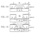
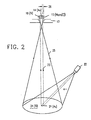
- FIG. 2 shows how these small dimensional relationships are provided in the preferred embodiment.
- FIG. 2 is provided for understanding only and is not to scale.
- FIG. 2 assumes that a crucible of gold or a crucible of titanium is made available within a suitable vacuum chamber for carrying out the process.
- the size of the gold crucible, and of the subsequently available titanium crucible, may be arbitrarily selected so long as a relatively small amount of gold surface or titanium surface is made available in line with the integrated circuit to be metallized.
- a spot 21 of gold is melted by an e-beam form e-beam generator 22 which is focused for a small spot.
- the small spot is centimeter, at a distance of 100 centimeters from the integrated circuit.
- the small gold melt provides an essentially unidirectional flow of gold metallization along path 23 through the window of photoresist 13 to provide gold corrosion barrier film 14 in an area defined by the opening in the surface of photoresist 13.
- the titanium metallization is carried out with a titanium crucible in essentially the same position but with e-beam generator 22 focused to a much larger melt (24) of titanium.
- the titanium melt is 2 centimeters in melt radius; the titanium melt is exaggerated in FIG. 2 to provide clarity in showing the relationship. Titanium metallization from this much larger melt source is focused along path 25 much less sharply than was gold corrosion barrier film 14.
- Thickness ranges for the metal depositions and oxide growth are shown in the following table:
- the corrosion resistance is not affected by thickness after minimums.
- corrosion barrier metals which may be used instead of gold, are:
- resistive metals which may be used instead of titanium, are:
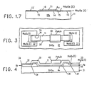
- FIG. 3 is a plan view of an elongated resistor utilizing the technology described in FIG. 1.
- FIG. 4 is a side-elevation view of the resistor structure 3.
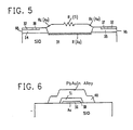
- FIG. 5 is a semi-schematic presentation of the same resistor.
- the entire resistor structure is arrayed on a silicon dioxide substrate 31 with niobium layers 34 and 35 appearing under their respective intrinsic oxides 32 and 33.
- Gold corrosion barrier film 36 extends from niobium area 34 to niobium area 35 across a bare spot on the surface of silicon dioxide substrate 31.
- Titanium resistive layer 39 bridges resistively between niobium area 34 and niobium area 35 and, in addition, provides a diffusion barrier extending over the unprotected surface of gold corrosion barrier film 36. Titanium resistive metal layer 39 and gold corrosion barrier film 36 thus provide a mutually protective structure.
- the gold corrosion barrier film 36 together with Nb 2 0 5 (E) passivating rings 37-38 provide a seal to prevent corrosive contact between titanium and niobium; at the same time titanium resistive metal layer 39 encapsulates the surface and edge of gold corrosion barrier film 36 to prevent diffusion problems.
- Resistor trimming is accomplished by a selective addition of lead-gold-indium solder shunt 40 which overlies the titanium but cannot diffuse through the titanium to cause diffusion problems with gold corrosion barrier film 36.
- FIG. 6 illustrates the encapsulating of the mutually protective corrosion barrier film 36 and the resistive metal layer 39 on silicon dioxide substrate 36.
- Lead-gold-indium solder 40 of the resistor trimming shunt is prevented by titanium resistive metal layer as a diffusion barrier from making contact with gold corrosion barrier film 36.
- the resistor is appropriate for superconductive use.
- Niobium layer 34 is superconductive at liquid helium temperatures while the gold titanium resistor 36/39 is resistive.
- Lead-gold-indium solder 40 is superconducting and forms a zero resistance shunt to a portion of the resistive length of titanium resistive metal structure 39.
- FIG. 5 shows the resistive relationships.
- the resistances of niobium metal areas 34 and 35 and of lead-gold-indium solder area 40 are each 00 at superconducting temperatures.
- the lead-gold-indium solder resistor trim shunts a portion of R(Ti) so as to trim the resistor to the desired value.
- R c (Au) is the quite small contact resistance through the gold barrier film between niobium metal 34-35 and titanium resistance metal 39.
- the very small resistance R c (Au) of the short path directly through corrosion barrier film 36 of gold are negligible except that they are not superconductive.
- the shunt resistance R(Au) of the gold corrosion barrier film in parallel to the resistance R(Ti) of the titanium resistive metal film 39 is not negligible and forms a part of the overall resistance value of the gold titanium resistor.
- FIG. 5 thus shows a gold/titanium resistive connection between two superconductive 34 and 35 comprising the resistance R(Au) of the gold corrosion barrier film and, parallel thereto, the resistance R(Ti) 39 of the titanium resistance layer.
- This Au/Ti composite resistor is partially shunted along a portion of its length by the zero resistance of the superconducting (PbAuln) trimming solder 40.
- the technique of this invention thus provides a minimum corrosion, trimmable diffusion resistant resistor structure with all process steps being self-aligned by the use of a single opening in a photoresist.
Landscapes
- Engineering & Computer Science (AREA)
- Manufacturing & Machinery (AREA)
- Superconductor Devices And Manufacturing Methods Thereof (AREA)
- Contacts (AREA)
Applications Claiming Priority (2)
| Application Number | Priority Date | Filing Date | Title |
|---|---|---|---|
| US454911 | 1982-12-30 | ||
| US06/454,911 US4459321A (en) | 1982-12-30 | 1982-12-30 | Process for applying closely overlapped mutually protective barrier films |
Publications (2)
| Publication Number | Publication Date |
|---|---|
| EP0114920A1 EP0114920A1 (en) | 1984-08-08 |
| EP0114920B1 true EP0114920B1 (en) | 1986-11-05 |
Family
ID=23806579
Family Applications (1)
| Application Number | Title | Priority Date | Filing Date |
|---|---|---|---|
| EP83106489A Expired EP0114920B1 (en) | 1982-12-30 | 1983-07-04 | Integrated circuit resistor structure |
Country Status (5)
| Country | Link |
|---|---|
| US (2) | US4459321A (enExample) |
| EP (1) | EP0114920B1 (enExample) |
| JP (1) | JPS59127323A (enExample) |
| CA (1) | CA1188428A (enExample) |
| DE (1) | DE3367486D1 (enExample) |
Families Citing this family (18)
| Publication number | Priority date | Publication date | Assignee | Title |
|---|---|---|---|---|
| US4700462A (en) * | 1986-10-08 | 1987-10-20 | Hughes Aircraft Company | Process for making a T-gated transistor |
| US4857418A (en) * | 1986-12-08 | 1989-08-15 | Honeywell Inc. | Resistive overlayer for magnetic films |
| US4754431A (en) * | 1987-01-28 | 1988-06-28 | Honeywell Inc. | Vialess shorting bars for magnetoresistive devices |
| DE59203408D1 (de) * | 1991-01-21 | 1995-10-05 | Siemens Ag | Verfahren zur Herstellung eines strukturierten Aufbaus mit Hochtemperatursupraleitermaterial. |
| US5474834A (en) * | 1992-03-09 | 1995-12-12 | Kyocera Corporation | Superconducting circuit sub-assembly having an oxygen shielding barrier layer |
| US5502002A (en) * | 1992-05-21 | 1996-03-26 | Hughes Aircraft Company | Polyimide passivation of GaAs microwave monolithic integrated circuit flip-chip |
| DE4320484A1 (de) * | 1993-06-21 | 1994-12-22 | Dornier Gmbh | Steuerbares Supraleiter-Bauelement |
| JP3360461B2 (ja) * | 1995-01-31 | 2002-12-24 | ソニー株式会社 | メタル成膜工程の前処理方法 |
| US5641611A (en) * | 1995-08-21 | 1997-06-24 | Motorola | Method of fabricating organic LED matrices |
| US6518673B2 (en) * | 2001-06-15 | 2003-02-11 | Trw Inc. | Capacitor for signal propagation across ground plane boundaries in superconductor integrated circuits |
| AU2003235349A1 (en) * | 2003-05-20 | 2004-12-13 | Fujitsu Limited | Electric contact device |
| US20060009038A1 (en) | 2004-07-12 | 2006-01-12 | International Business Machines Corporation | Processing for overcoming extreme topography |
| US7135377B1 (en) * | 2005-05-20 | 2006-11-14 | Phoenix Precision Technology Corporation | Semiconductor package substrate with embedded resistors and method for fabricating same |
| US7615385B2 (en) | 2006-09-20 | 2009-11-10 | Hypres, Inc | Double-masking technique for increasing fabrication yield in superconducting electronics |
| TWI614916B (zh) * | 2013-11-11 | 2018-02-11 | Epistar Corporation | 光電元件及其製造方法 |
| JP6252123B2 (ja) * | 2013-11-14 | 2017-12-27 | 日亜化学工業株式会社 | 発光素子の製造方法 |
| CN104659175A (zh) * | 2013-11-15 | 2015-05-27 | 晶元光电股份有限公司 | 光电元件及其制造方法 |
| WO2015074665A1 (en) * | 2013-11-20 | 2015-05-28 | Danmarks Tekniske Universitet | Method for producing substrates for superconducting layers |
Family Cites Families (15)
| Publication number | Priority date | Publication date | Assignee | Title |
|---|---|---|---|---|
| GB492580A (en) * | 1937-10-26 | 1938-09-22 | Torrington Mfg Co | Improvements in or relating to devices for forming or bending wound springs |
| US3386906A (en) * | 1965-11-26 | 1968-06-04 | Philips Corp | Transistor base and method of making the same |
| US3754168A (en) * | 1970-03-09 | 1973-08-21 | Texas Instruments Inc | Metal contact and interconnection system for nonhermetic enclosed semiconductor devices |
| US3701931A (en) * | 1971-05-06 | 1972-10-31 | Ibm | Gold tantalum-nitrogen high conductivity metallurgy |
| US3907620A (en) * | 1973-06-27 | 1975-09-23 | Hewlett Packard Co | A process of forming metallization structures on semiconductor devices |
| US3877063A (en) * | 1973-06-27 | 1975-04-08 | Hewlett Packard Co | Metallization structure and process for semiconductor devices |
| US3913120A (en) * | 1973-12-28 | 1975-10-14 | Ibm | Thin film resistors and contacts for circuitry |
| CH587567A5 (en) * | 1975-08-28 | 1977-05-13 | Ibm | Josephson contact tunnel layer - is produced in reactor on base electrode and followed by counter electrode without interruption |
| US4075756A (en) * | 1976-06-30 | 1978-02-28 | International Business Machines Corporation | Process for fabricating above and below ground plane wiring on one side of a supporting substrate and the resulting circuit configuration |
| US4316200A (en) * | 1980-03-07 | 1982-02-16 | International Business Machines Corporation | Contact technique for electrical circuitry |
| US4310569A (en) * | 1980-03-10 | 1982-01-12 | Trw Inc. | Method of adhesion of passivation layer to gold metalization regions in a semiconductor device |
| JPS5722216A (en) * | 1980-07-17 | 1982-02-05 | Nippon Kogaku Kk <Nikon> | Observing device for cylindrical inside wall |
| JPS5735341A (en) * | 1980-08-12 | 1982-02-25 | Toshiba Corp | Method of seperating elements of semiconductor device |
| US4421785A (en) * | 1980-08-18 | 1983-12-20 | Sperry Corporation | Superconductive tunnel junction device and method of manufacture |
| EP0088808B1 (en) * | 1982-03-12 | 1985-11-21 | International Business Machines Corporation | Process for producing niobium josephson junctions |
-
1982
- 1982-12-30 US US06/454,911 patent/US4459321A/en not_active Expired - Lifetime
-
1983
- 1983-07-04 DE DE8383106489T patent/DE3367486D1/de not_active Expired
- 1983-07-04 EP EP83106489A patent/EP0114920B1/en not_active Expired
- 1983-07-14 JP JP58127053A patent/JPS59127323A/ja active Granted
- 1983-09-16 CA CA000436857A patent/CA1188428A/en not_active Expired
-
1984
- 1984-03-16 US US06/590,319 patent/US4504552A/en not_active Expired - Fee Related
Also Published As
| Publication number | Publication date |
|---|---|
| US4459321A (en) | 1984-07-10 |
| DE3367486D1 (en) | 1986-12-11 |
| JPH0144024B2 (enExample) | 1989-09-25 |
| CA1188428A (en) | 1985-06-04 |
| US4504552A (en) | 1985-03-12 |
| JPS59127323A (ja) | 1984-07-23 |
| EP0114920A1 (en) | 1984-08-08 |
Similar Documents
| Publication | Publication Date | Title |
|---|---|---|
| EP0114920B1 (en) | Integrated circuit resistor structure | |
| CA1140682A (en) | Intermetallic barrier region for gold conductor contacts | |
| JPH01321612A (ja) | 重ね合わせたかカプセル化した金属導電路を提供する方法 | |
| CA1142264A (en) | Contact technique for electrical circuitry | |
| US4319264A (en) | Nickel-gold-nickel conductors for solid state devices | |
| JPS58200586A (ja) | ニオブ−絶縁体−ニオブのジヨセフソンのトンネル接合デバイスのその場製造の方法 | |
| WO1997015955A1 (en) | High temperature superconducting josephson junctions and squids | |
| JPS6329961A (ja) | 薄膜受動回路の製造方法とその方法によって製造される薄膜受動回路 | |
| US4817854A (en) | LED soldering method utilizing a PT migration barrier | |
| US5926360A (en) | Metallized oxide structure and fabrication | |
| JPH07221181A (ja) | 半導体素子の金属配線の形成方法 | |
| EP0419361A2 (en) | Electrode for electrical connection to oxide superconductor and method for forming the same | |
| JPH0472764A (ja) | 半導体装置の裏面電極 | |
| JP2720442B2 (ja) | 磁気抵抗素子の製造方法 | |
| JPH11163026A (ja) | ワイヤボンディング方法 | |
| JPS60160120A (ja) | 半導体素子用電極の形成方法 | |
| JPH01253257A (ja) | 半導体集積デバイス | |
| JPS6221283A (ja) | 超伝導集積回路 | |
| JP2682928B2 (ja) | 磁気抵抗素子 | |
| JPH0243727A (ja) | 半導体装置の製造方法 | |
| JP2535539B2 (ja) | ジョセフソン回路の製造方法 | |
| JPS58125881A (ja) | 縦型抵抗回路の構成方法 | |
| JPS6059742B2 (ja) | 半導体装置およびその製造方法 | |
| JPH09260379A (ja) | 半導体装置およびその製造方法 | |
| JPH0349661B2 (enExample) |
Legal Events
| Date | Code | Title | Description |
|---|---|---|---|
| PUAI | Public reference made under article 153(3) epc to a published international application that has entered the european phase |
Free format text: ORIGINAL CODE: 0009012 |
|
| AK | Designated contracting states |
Designated state(s): DE FR GB IT |
|
| 17P | Request for examination filed |
Effective date: 19841029 |
|
| 17Q | First examination report despatched |
Effective date: 19860120 |
|
| GRAA | (expected) grant |
Free format text: ORIGINAL CODE: 0009210 |
|
| AK | Designated contracting states |
Kind code of ref document: B1 Designated state(s): DE FR GB IT |
|
| REF | Corresponds to: |
Ref document number: 3367486 Country of ref document: DE Date of ref document: 19861211 |
|
| ET | Fr: translation filed | ||
| ITF | It: translation for a ep patent filed | ||
| PLBE | No opposition filed within time limit |
Free format text: ORIGINAL CODE: 0009261 |
|
| STAA | Information on the status of an ep patent application or granted ep patent |
Free format text: STATUS: NO OPPOSITION FILED WITHIN TIME LIMIT |
|
| 26N | No opposition filed | ||
| ITTA | It: last paid annual fee | ||
| PGFP | Annual fee paid to national office [announced via postgrant information from national office to epo] |
Ref country code: FR Payment date: 19920630 Year of fee payment: 10 |
|
| PGFP | Annual fee paid to national office [announced via postgrant information from national office to epo] |
Ref country code: DE Payment date: 19920729 Year of fee payment: 10 |
|
| PGFP | Annual fee paid to national office [announced via postgrant information from national office to epo] |
Ref country code: GB Payment date: 19930622 Year of fee payment: 11 |
|
| PG25 | Lapsed in a contracting state [announced via postgrant information from national office to epo] |
Ref country code: FR Effective date: 19940331 |
|
| PG25 | Lapsed in a contracting state [announced via postgrant information from national office to epo] |
Ref country code: DE Effective date: 19940401 |
|
| REG | Reference to a national code |
Ref country code: FR Ref legal event code: ST |
|
| PG25 | Lapsed in a contracting state [announced via postgrant information from national office to epo] |
Ref country code: GB Effective date: 19940704 |
|
| GBPC | Gb: european patent ceased through non-payment of renewal fee |
Effective date: 19940704 |