EP0104477A2 - Verfahren zur Bilduntersuchung - Google Patents
Verfahren zur Bilduntersuchung Download PDFInfo
- Publication number
- EP0104477A2 EP0104477A2 EP83108547A EP83108547A EP0104477A2 EP 0104477 A2 EP0104477 A2 EP 0104477A2 EP 83108547 A EP83108547 A EP 83108547A EP 83108547 A EP83108547 A EP 83108547A EP 0104477 A2 EP0104477 A2 EP 0104477A2
- Authority
- EP
- European Patent Office
- Prior art keywords
- data
- sample
- decision
- picture element
- Prior art date
- Legal status (The legal status is an assumption and is not a legal conclusion. Google has not performed a legal analysis and makes no representation as to the accuracy of the status listed.)
- Granted
Links
Images







Classifications
-
- B—PERFORMING OPERATIONS; TRANSPORTING
- B41—PRINTING; LINING MACHINES; TYPEWRITERS; STAMPS
- B41F—PRINTING MACHINES OR PRESSES
- B41F33/00—Indicating, counting, warning, control or safety devices
- B41F33/0036—Devices for scanning or checking the printed matter for quality control
-
- G—PHYSICS
- G06—COMPUTING OR CALCULATING; COUNTING
- G06T—IMAGE DATA PROCESSING OR GENERATION, IN GENERAL
- G06T7/00—Image analysis
- G06T7/0002—Inspection of images, e.g. flaw detection
-
- G—PHYSICS
- G06—COMPUTING OR CALCULATING; COUNTING
- G06T—IMAGE DATA PROCESSING OR GENERATION, IN GENERAL
- G06T7/00—Image analysis
- G06T7/0002—Inspection of images, e.g. flaw detection
- G06T7/0004—Industrial image inspection
-
- G—PHYSICS
- G06—COMPUTING OR CALCULATING; COUNTING
- G06T—IMAGE DATA PROCESSING OR GENERATION, IN GENERAL
- G06T7/00—Image analysis
- G06T7/0002—Inspection of images, e.g. flaw detection
- G06T7/0004—Industrial image inspection
- G06T7/001—Industrial image inspection using an image reference approach
-
- G—PHYSICS
- G06—COMPUTING OR CALCULATING; COUNTING
- G06T—IMAGE DATA PROCESSING OR GENERATION, IN GENERAL
- G06T7/00—Image analysis
- G06T7/70—Determining position or orientation of objects or cameras
- G06T7/73—Determining position or orientation of objects or cameras using feature-based methods
- G06T7/74—Determining position or orientation of objects or cameras using feature-based methods involving reference images or patches
-
- G—PHYSICS
- G06—COMPUTING OR CALCULATING; COUNTING
- G06V—IMAGE OR VIDEO RECOGNITION OR UNDERSTANDING
- G06V10/00—Arrangements for image or video recognition or understanding
- G06V10/98—Detection or correction of errors, e.g. by rescanning the pattern or by human intervention; Evaluation of the quality of the acquired patterns
- G06V10/993—Evaluation of the quality of the acquired pattern
-
- G—PHYSICS
- G07—CHECKING-DEVICES
- G07D—HANDLING OF COINS OR VALUABLE PAPERS, e.g. TESTING, SORTING BY DENOMINATIONS, COUNTING, DISPENSING, CHANGING OR DEPOSITING
- G07D7/00—Testing specially adapted to determine the identity or genuineness of valuable papers or for segregating those which are unacceptable, e.g. banknotes that are alien to a currency
- G07D7/06—Testing specially adapted to determine the identity or genuineness of valuable papers or for segregating those which are unacceptable, e.g. banknotes that are alien to a currency using wave or particle radiation
- G07D7/12—Visible light, infrared or ultraviolet radiation
-
- G—PHYSICS
- G06—COMPUTING OR CALCULATING; COUNTING
- G06T—IMAGE DATA PROCESSING OR GENERATION, IN GENERAL
- G06T2207/00—Indexing scheme for image analysis or image enhancement
- G06T2207/30—Subject of image; Context of image processing
- G06T2207/30108—Industrial image inspection
- G06T2207/30144—Printing quality
Definitions
- the present invention relates to a method and device for inspecting a printed image.
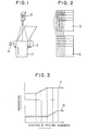
- a line sensor camera 2 scans a printed image 1 in the widthwise direction as shown in FIG. 1 so that image information is derived.
- the angle of rotation of a transfer cylinder 3 is detected by a rotary encoder 4 attached thereto so that in response to the output from the encoder 4, the scanning by the camera 2 is synchronized so that a sample image 5 (See FIG. 2) is divided into a plurality of picture elements in the form of a matrix.
- a reference image 6 (See FIG. 2) is also divided into a plurality of picture elements in the form of a matrix. The density of each picture element of the sample image 5 is compared with the density of each picture element of the reference image 6, whereby whether the sample image 5 has defective picture elements or not is detected.
- the graduation 7 of three picture elements (marked by 0) of the sample image 5 are different from the graduation 8 of the corresponding picture elements of the sample image 5 .
- the sample image 5 has no defective picture element, it is detected as unacceptable or as having defective picture elements.
- One of the methods to overcome this problem is to provide a large degree of graduation difference tolerance; that is, the tolerance in graduation between the reference and sample images 6 and 5, but this method is not satisfactory in practice because the defects of the sample image cannot be detected with a satisfactorily high degree of accuracy.
- the present invention was made to overcome the above and other problems encountered in the prior art methods and devices for inspecting printed images arid has for its object to provide a method and device for inspecting printed images, whereby even when a printed image is deviated in any direction, it may be inspected with-a high degree of accuracy.
- Another object of the present invention is to provide a device for inspecting printed images which is inexpensive to manufacture yet highly reliable and dependable in operation.
- a method and device for inspecting printed images in which when widthwise image graduation data of a sample image (to be referred to as “the sample row datum or data” in this specification) is compared with the corresponding widthwise image graduation data of a reference image (to be referred to as “the reference row datum or data” in this specification) so as to detect the defective picture elements of the sample image, each sample row datum is compared with a plurality of reference row data which are shifted within a predetermined tolerance range so that the sample row data are compared with the reference row data which are most similar in phase with the sample row data.
- FIGS. 4a, 4b and 4c are shown a sample row data and a reference row data.
- FIG. 4a shows the fundamental relationship between the sample row data and the reference row data;
- FIG. 4b shows the relationship between the deviation in position between the sample and reference row data;
- FIG. 4c shows the relationship between the sample and reference row data at the edge of an image or other special portion thereof.
- one sample row datum 9 is compared with a plurality of reference row data 10-16 which are obtained by shifting to the right and left the reference row datum 13 by a distance corresponding to one picture element based upon a deviation in position expected to result from the tolerance of a transport system.
- the datum 12 which is most similar in phase to the sample row datum 9 is compared in density with the sample row datum 9, whereby a defect can be detected.
- a method for choosing the reference row datum from the reference row data which is most similar in phase to the sample row datum is as follows.
- the reference row datum which is most similar in phase to the sample row datum finds the least number of defects as shown in FIG. 4b. That is, the reference row datum which finds the least number of defects during one horizontal scanning period is one which is most similar in phase to the sample row datum.
- FIG. 4b shows an image with a relatively low degree of contrast and if an image has a relatively high degree of contrast, the curve would become steeper.
- a sample row datum 17 is compared with a reference row datum 18 which is most similar in phase to the sample row datum 17.
- a large graduation tolerance is given. Therefore, the defects at an edge at which the graduation difference is high can be suitably detected. That is, the reference row datum 18 is most similar in phase to the sample row datum 17 so that the phase difference between them is one half of a picture element. Therefore, a tolerance for a picture element at an edge is the graduation difference between the reference and sample row data which are spaced apart from each other by one half of a picture element.
- FIG. 5 a first embodiment of the present invention based upon the underlying principle described with reference to FIG. 4.
- a camera 2 scans a print 1, whereby image information can be derived.
- a rotary . encoder 4 detects the angle of rotation of a transport cylinder 3 and applies its output to a sync circuit 21.
- the output from the sync circuit 21 is applied to the camera 2, an A/ D converter 22 and an address circuit 24 so that the scanning by the camera 2 can be synchronized; and A/D conversion of the image information derived from the camera 2 can be synchronized; and the addressing to a reference picture element data memory 25 and a picture element control data memory 26 can be carried out.
- the writing of the reference row data into the reference picture element data memory 25 and the readout of the data from the reference picture element data memory 25 and the picture element control data memory 26 in order to activate a decision circuit .23 so as to detect the sample row data can be synchronized.
- the picture element data memory 26 stores a tolerance for each picture element.
- the decision circuit 23 compares the sample row data with the reference row data, it takes into consideration a tolerance supplied from the picture element control data memory 26.
- each shift circuit carries out the shift operation. To this end, one clock CLK is generated for each picture element.
- the sample row datum TD1 is sequentially shifted in synchronism with the scanning by the camera 2 by the latches L 4 , L 5 and L 6 so that TD 2, TD3 and TD4 may be derived.
- the reference row datum SD; and the picture element control datum MD1 are sequentially shifted by the latches L 1 , L 2 and L 3 so that MD2, MD3, MD4, SD2, SD3 and SD4 are derived.
- the sample row datum TD1 is applied to the decision elements JEl, JE2, JE3 and JE4 and compared with the reference row datum and the picture element control datum. That is, the decision element JE4 compares the sample row datum TD1 with the reference row datum SD1 and the picture element control datum MDl.
- the decision element JEl compares TDl with SD2 and MD2; the decision element JE2 compares TD1 with SD3 and MD3; and the decision element JE3 compares TD1 with SD4 and MD 4. Therefore, the decision is made when the reference row datum and the picture element control datum are delayed with respect to the sample row datum.
- the decision elements JE5, JE6 and JE7 make decisions when the sample row data are delayed with respect to the reference row data and the picture element control data.
- each of the decision elements JEl - JE7 compares the sample row datum 9 with each of the reference row data 10 - 16 (See FIG. 4a).
- the outputs from the decision elements JEl - JE7 are applied to an overall decision circuit TJU which selects the least output and compares it with a predetermined threshold value. That is, depending upon whether the least output is higher or lower than the threshold value, the printed image is rejected or accepted.
- each of decision elements JE comprising a detector DA for detecting the absolute value of a difference, a comparator CP and a counter CT.
- the absolute value /TD - SD/ between the sample row datum TD and the reference row datum SD is derived from the detector DA and the absolute value /TD - SD/ is compared with a picture element control data MD, which is a tolerance for /TD - SD/, in the comparator CP the output of which is applied to the counter CT, whereby the number of picture elements in which /TD - SD/ > MD is counted.
- FIG. 8 is shown in detail the construction of the detector DA shown in FIG. 7.
- the detector DA comprises two adders AD1 and AD2, an exclusive-or circuit EX and an inverter INV. Inputs TD and SD are applied to the first adder AD1 and the output TD - SD is derived from the second adder AD2.
- the detector DA of this type is well known in the art so that no further detailed explanation shall be made in this specification.
- F IG. 9 is shown in detail the construction of the overall decision circuit TJU comprising six low-or minimum-value detectors MINI - MIN6 so that the least or minimum output is detected from the outputs Jl - J7 from the decision elements JEl - JE7 (See FIG. 6).
- the low- or minimum-value detector MIN comprising a selector SE and a comparator CP.
- the detector MIN is adapted to detect whether the input A is lower than the input B or the input B is lower than the input A. Therefore, in the overall deci- / sion circuit TJU, the first detector MINI detects whether the input Jl is lower than the input J2, the second detector MIN2 detects whether the input J3 is lower than the input J4 or the input J4 is lower than the input J3 and the third detector MIN3 detects whether the input J5 is lower than the input J6 or the input J6 is lower than J5.
- the fourth detector MIN4 detects whether the output from the detector MIN1 is lower than the output from the detector MIN2 or vice versa and the fifth detector MIN5 detects whether the output from the third detector MIN3 is lower than the input J7 or vice versa. Finally the sixth detector MIN6 detects whether the output from the fourth detector MIN4 is lower than the output from the fifth detector MIN5 or vice versa. Thus, the least or minimum output among the inputs Jl through J7 is derived from the sixth detector MIN6.
- the reference row data are compared with the sample row data so that the inspection can be carried out with a higher degree of accuracy as compared with the case in which the whole sample print is compared with the whole reference print.
- FIG. 11 is shown a circuit diagram which is capable of compensating for the deviation in position in the direction of the transportation of the'print.
- the circuit comprises decision circuits JCl - JC7, shift registers SRl - SR6 and an overall decision circuit TJU.
- Each of the shift registers SR has the number of bits equal to the number of bits of the sensor array of the camera 2 (See FIG. 1).
- the shift registers SRl - SR6 are similar in function to the latches Ll - L6 as shown in FIG. 6.
- FIG. 12 is shown another embodiment of the present invention.
- the camera 2 scans the printed image 1 so that printed image information is derived.
- the rotary encoder 4 detects the angle of rotation of the transport cylinder 3 and the output from the rotary encoder 4 is applied to a sync circuit 121.
- the output from the sync circuit 121 is applied to the camera 2, an A/ D converter 122 and an address circuit 124 so that the scanning by the camera 2 can be synchronized; the A/D con- vertions of the image information derived from the camera 2 can be synchronized; and the addressing of a reference data memory 125 and a picture element control data memory 126 is accomplished.
- a switch SW is so actuated that a reference datum S is read out from the reference data memory 125 for each sample datum T and a picture element control datum M is read out from the picture element control memory 126.
- the picture element control datum M represents a tolerance for each picture element.
- the reference datum S derived from the memory 125, the picture element control datum M derived from the memory 126 and the sample datum T derived from the A/D converter 122 are applied to a positional deviation correction circuit 123 so that S', M' and T' are derived and applied to a decision circuit 127.
- the decision circuit 127 detects the defects of the image on the sample print.
- FIG. 13 is shown in detail the construction of a correlator which constitutes the positional deviation correction circuit 123 (FIG. 14).
- a correction circuit (FIG. 15) corrects a positional deviation.
- the correlator 130 may comprise, for example, TDC 1023J, the product of TRW Corp.
- the correlator 130 comprises two 64-bit shift registers 131 and 132, one 64 -bit latch 133, exclusive-nor gates ENOR 1 - ENOR 64 and an adder 134.
- One-bit serial input B IN (64 bits) and clock CLKB for effecting the serial input are applied to the shift register 132 and each bit output is applied to the latch 133 (R1 - R64) which in turn is latched in response to the latch signal LDR.
- One-bit serial input A IN (64 bits) and clock CLKA for effecting the serial input are applied to the shift register 131.
- Each bit output is applied to one input terminal of each of exclusive-or gates ENOR 1 - ENOR 64 .
- the bit output from the latch 133 (R 1 - R 64 ) is applied to the other input of the exclusive-or gate.
- the sample data A l -A 64 are applied to the shift register 131 and to the exclusive-NOR gates ENOR 1 - ENOR 64 to which are also applied the reference data R 1 - R 64 from the latch 133.
- An equals Rn
- the output from the exclusive-NOR gate ENOR n is "1"
- An is not equal to Rn
- the output is "0”.
- the number of the exclusive-NOR gates which delivers "1” are derived from the adder 134 as the correlated value. Therefore the maximum value of the correlated value is "64".
- the correlated value varies. That fact that the sample data A are in phase with the reference data R means that the correlated value has a miximum value. It follows therefore that positional deviation can be detected by determining the phase at which the correlated value has a maximum value.
- FIG. 14 is shown in detail the construction of the positional deviation detector which utilizes the correlator 130 as shown in FIG. 13.
- the positional deviation range which can be detected can be easily expanded as will be described hereinafter.
- the correlationship between the time serial l/ ⁇ patterns of MSBS 7 and T 7 is determined by the correlator 130.
- the mode of operation of the circuit as shown in FIG. 14 will be described in more detail hereinafter. It is assumed that the reference datum S and the sample datum T both having the same address be simultaneously applied. In order to detect that sample datum T is advanced, the sample datum T 7 is applied to an 8-bit shift register 141 and is delayed in phase by 8 bits.
- the camera scanning clock CLK may be used to shift the shift register 141.
- the counter 142 delivers the latch signal LDR for latching the pattern.
- the latch 144 holds the correlated value Corr.
- the initial value of the latch 144 is ⁇ when the scanning by the camera 2 is started and is reset in response to the scanning start signal S ZERO produced by a system. Whenever a high correlated value Corr is delivered from the correlator 130, it is latched in the latch 144 in response to the output from the comparator 145.
- the counter 143 counts the camera scanning clock CLK and the count or result (4 bits representative of the numbers from 0 - 15) is stored in the latch 146.
- the content in the latch 146 is varied everytime when a high correlated value Corr is delivered in response to the output from the comparator 145 so that the phase when the correlated value has a maximum value is stored in the latch 146.
- the positional deviation D (-8 - +7) can be obtained by subtracting "8" from the maximum correlated value Corr latched in the latch 146 by a subtractor 147. The subtraction of "8" is made in order to correct the delay in the shift register 141 corresponding to 8 clocks CLK counted by the counter 143.
- the counter 143 and the latch 144 are reset so that the positional deviation D representative of the positional difference between the reference datum S and the sample datum T is derived. That is, if the total number of picture elements scanned by the camera is 512, the correction of the positional deviation between the reference datum S and the sample datum T can be carried out for every 8 blocks each consisting of 64 picture elements.
- a 16-bit shift register 145 is used and the counter 143 is so modified that it delivers the output consisting of 8 bits. And "16" is subtracted by the subtractor 147.
- the positional deviation D (-16 +15) can be obtained.
- the range of the positional deviation D which can be detected can be expanded.
- FIG. 15a and FIG. 15b is shown in detail a positional deviation correction circuit which is adapted to correct a positional deviation in response to the output D from the positional deviation detector as shown in FIG. 14.
- FIG. 15a shows a circuit which processes the sample datum T
- the reference datum S; the sample datum T; and the picture element control datum M' whose positional deviations are corrected can be derived.
- the corrected S', T' and M' are applied to the decision circuit 127 (See FIG. 12) so that defects can be detected.
- FIG. 16 is shown one example of the decision circuit 127.
- 157 - 162 are 8-bit latches; 163, an OR gate array which is adapted to receive 8 bits; 164, a shift register; 165, a selector; 166 and 169, adders; 167, an inverter; 168, an exclusive OR gate; and 170, a comparator.
- the datum D is applied from the latch 162 to one input terminal B of the comparator 170.
- the reference datum S' derived from the latch 158 is applied to the shift register 164 in which the reference datum S' is shifted by a predetermined number of bits and is multiplied by a coefficient K (which is less than unity) so that KS' is applied to one input terminal B of the selector 165.
- the picture-element control datum M' is applied through the latch 157 to the other input terminal A of the selector 165 and through the OR gate 163 to the selection terminal S of the selector 165.
- the selector 165 is adapted to deliver the datum applied to the input terminal B when the signal applied to the selection terminal S is at a high level, but when the signal applied to the selection terminal S is at a low level, the datum applied to the input terminal A is delivered as the output.
- the comparator 170 compares the datum JL applied to the input terminal A with the datum D applied to the input terminal B and delivers a high-level output J only when the datum applied to the input terminal B is greater than the datum applied to the input terminal A. That is, the datum JL applied to the input terminal A is used as a reference level and the output J is derived in the manner described above.
- sample data memory may be provided.
- the sample data may be displaced by one picture element in the direction in which the print is transported.
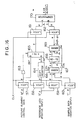
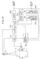
- FIG. 17 is shown a third embodiment of the present invention.
- the rotary encoder 4 detects the angle of rotation of the transport cylinder 3 which transports the print 1 and the output from the encoder is applied to a sync circuit 221.
- the scanning position signal from the camera 2 is also applied to the sync circuit 221 so that a position on the print 1 is detected.
- an A/D converter 222 converts the analog output from the camera 2 into a digital signal.
- an address correction circuit 224 addresses the print 1. The most important function of the address correction circuit 224 is to determine an optimum address of the next row in response to the feedback of the output from a decision circuit 223 regarding to the reference row patten which is most similar in phase to the sample row pattern.
- a digital quantity is detected and the information for each picture element is stored in a reference picture element data memory 225.
- the decision circuit 223 compares with sample row data with the shift row data derived from the reference picture element data memory 225 in a real time.
- a decision level setting circuit 227 obtains a decision level in a real time and the output from the decision level setting circuit 227 is applied to the decision circuit 223.
- the signal (which is indicated by the broken line) which is applied from the address correction circuit 224 to the decision circuit 223 is used to obtain an optimum address of the sample picture element datum derived from the camera 2.
- the decision circuit 223 must be provided with a shift register or the like so that the sample picture element data must be shifted one picture element by one picture element.
- FIG. 18 is shown in detail the construction of the decision circuit 223 when the shift is ⁇ 3 picture elements and one line consists of 512 picture elements.
- the decision circuit 223 consists of a shift circuit consisting of latches L l - L 3 for shifting by one picture element the reference row datum SD and the decision level datum MD and another shift circuit consisting of latches L 4 - L 6 for shifting by one picture element the sample row datum TD. These shift circuits are combined with decision elements JE 1 - JE 7 .
- the sample row datum TD1 is shifted by the latches L 4 , L 5 and L 6 in synchronism with the camera scanning, whereby TD2, TD3 and TD4 are derived.
- the reference row datum SD1 and the decision level datum MD1 are shifted by the latches L 1 , L 2 and L 3 so that the MD2, MD3 and MD4 and SD2, SD3 and SD4 are derived.
- the sample row datum TD1 is applied to the decision elements JE1, JE2, JE3 and JE4 and is compared with the reference row datum and the decision level datum. That is, the decision element JE4 compares the sample row datum TD1 with the reference row datum SD1 and the decision level datum MDl; the decision element JEl compares TD1 with SD2 and MD2; the decision element JE2 compares TD1 with SD3 and MD3; and the decision element JE3 compares TD1 with SD4 and MD4. Therefore the decision is made when the reference row datum and the decision level datum are delayed with respect to the sample row datum.
- the decision elements JEl - JE7 compare the sample row datum 9 with the reference row data 10 - 16 (See FIG. 4a). In this case the outputs from the decision elements JEl - JE7 represent the number of defects detected during one scanning by the camera 2.
- the outputs from these seven decision elements JE1 - JE7 are applied to an overall decision circuit TJU which selects the minium number of defects from the numbers of defects derived from the decision elements JEl - JE7 and compares the selected minimum number of defects with a threshold value, thereby making the decision whether good or bad. That is, the sample row datum and the reference row datum which is most similar in phase to the sample row datum are compared.
- the decision element which gives the minimum number of defects is detected. As a result, it can be detected how many picture elements the sample row datum being inspected is spaced or deviated from the reference row datum.
- the discrimination datum is applied from the output terminal ST to the address correction circuit 224 so that the first address of the next camera scanning is determined.
- FIG. 19 is shown in detail the construction of a decision element JE used in the decision circuit as shown in FIG. 18.
- the decision element JE comprises a detector DA for detecting the absolute value of a difference, a comparator CP, a counter CT and a latching circuit LA.
- the detector DA is substantially similar in construction to that as shown in FIG. 8. That is, the detector DA obtains the absolute value of the difference /TD - SD/ between the sample row datum TD(TD 1 - TD 4 ) and the reference row datum SD(SD . - SD 4 ).
- the comparator CP compares /TD - SD/ with the decision level MD(MD 1 - MD 4 ) derived from the decision level setting circuit 227.
- a picture element in excess of a decision level is applied as a defect signal to the counter CT.
- the counter CT is reset everytime when the scanning start signal SZERO is produced when one scanning by the camera 2 is started. Therefore the counter CP counts only when the defect signals are produced.
- the clock CLK applied to the counter CT is the clock which is used to attain the timing in the inspection device in accordance with the present invention.
- One clock corresponds to one picture element being scanned. That is, the counter CP counts the number of defective picture elements detected during one scanning time period by the camera 2.
- the latch LA responds to the scanning end signal SEND produced every time when one scanning is accomplished and delivers to the overall decision circuit TJU the number of defective picture elements detected during one scanning time period as a signal FN (FNl - FN7).
- FIG. 20 is shown in detail the construction of the overall decision circuit TJU comprising six low- or minimum-value detectors MIN1 -MIN6, a comparator CP and a decision element descrimination circuit JA.
- the comparator CP compares the thus detected minimum defect number with a given defect tolerance number.
- the row which has defects in excess of a predetermined defect tolerance number is detected as a defective row and the detection signal is derived from the output terminal OUTPUT.
- a predetermined defect tolerance number consists of a maximum number of defects below which the quantity of a print is judged acceptable, plus a predetermined marginal number which is added in order to prevent the misjudgement due to noise or the like.
- the overall decision circuit TJU includes the decision element discrimination circuit JA in order to detect which sample row datum is most similar in phase (has a minimum number of defects) to reference row data.
- the output ST from the discrimination circuit JA therefore represents how many picture elements the point being scanned is deviated from the reference row datum applied to the inspection device.
- FIG. 22 is shown in detail the construction of the decision element discrimination circuit JA comprising inverters INVl - INV6, OR gates ORl - OR6 and an encoder EN.
- the method for setting a decision level (See Japanese Patent Application No. 179,599/1981 filed by the same applicant) has been further improved so that the decision circuit makes a decision in a real time and makes no wrong decision at all.
- the first decision level is called “a fixed level” and assigned with a minimum value representing a shadow portion (the lowest density portion) of an image or with a maximum value (8 bits, 255) representing a portion (margin) which is not needed to be inspected.
- the first decision level is stored in the decision level data memory 226.
- the second decision level is called “a proportional level” and is a value of a datum derived from the reference picture element data memory 225 which is multiplied by K (K ⁇ 1). The second decision level serves to improve the inspection.
- the third decision level is called "edge level" and represents the difference between the adjacent picture elements in the reference picture element data memory 225. It serves to prevent erratic operations when the density changes rapidly.
- the second and third decision levels are calculated in real time from data derived from the reference picture element data memory 225.
- the maximum level is assigned, whereby the erratic detection can be avoided. That is, when the differences in level between picture elements in the reference picture element datum SD are small, the first decision level is used. When the differences in level between the picture elements are high due to graduation, the second decision level is used. When the differences in level between the picture elements are remarkably high because of an edge portion, the third decision level is used. Thus, misjudgement can be avoided.
- FIG. 23 is shown in detail the construction of the decision level setting circuit 227.
- the difference between the adjacent picture elements can be obtained by means of latching circuits LA3 and LA4, an inverter INV and detectors DA2 and DA3 each for obtaining or determining the absolute value of a difference.
- the higher one of the adjacent picture elements is applied through a high-value detector HL1 to the B input terminal of a high-value detector HL2 as a level for determining "the edge level". Therefore, when one picture element is compared with the right or left picture element, one decision level may be assigned even when the position of a picture element is deviated to the right or left.
- the reference picture element datum SD is multiplied with K (K ⁇ 1) by a proportional level setting circuit RS and applied to the-input terminal C of the high-value detector HLC2 as a level for determining a proportional level.
- the reference picture element datum SD is derived as the ouput from the latching circuit LA4 so that "the edge level” may coincide in phase with a picture element.
- latching circuits L A1 and LA2 are used to coincide phases and the output from the latch LA2 is applied to the input terminal A of the high-value detector HL2.
- the high-value detector HL 2 detects the highest level of the inputs A, B and C; that is, an optimum level obtained from the difference in level between the picture elements in the region of the reference picture element datum SD. The highest or optimum level is applied to the decision circuit 227 as a decision level MD of that-picture element.
- the above operation is carried out in synchronism with the timing clock CLK of the inspection device so that the decision level is applied in real time to the decision circuit which compares the picture elements of the sample row datum with those of the reference row datum.
- the detectors DA2 and DA3 are substantially similar in construction to that as shown in FIG. 8.
- the high-value detectors HL1 and HL2 have the function opposite to the function of the low-value priority circuit MIN so that the circuit diagram of the high-value detector HLl or HL2 is now shown in the drawing.
- FIG. 24 is shown in detail the construction of the proportional level setting circuit RS.
- no multiplier is used.
- a decoder DE is used to select gates Gl - G4 so that a specific decision level may be obtained.
- the proportional level setting value consists of two bits. Of the inputs to the gate Gl, the most significant bit is connected to LOW while the lower seven bits are connected to the upper seven bits of the reference picture element datum SD (the remaining one bit being not connected). Therefore, when the gate Gl is selected, 50% of the reference picture element datum SD is derived. In like manner, when G2 is selected, 25% of the reference picture element data SD is derived; when G3 is selected, 12.5% of the reference picture element data SD is derived; and when G4 is selected, 6.25% of the reference picture element datum SD is derived.
- the address at which the scanning is started is so shifted that the misalignment between the scanning lines may be reduced to a minimum.
- the load imposed on the hardware may be considerably decreased. This will be described in detail with reference to FIG. 26.
- the address correction is made based upon the point at which the scanning is started and the point at which the scanning is terminated.
- the angle of rotation of the cylinder 3 is divided based on the signal derived from the rotary encoder 4.
- the points at which the scanning is started are designated by N1 and N2 while the points at which the scanning is terminated are designated by ED1 and ED2. Every time when the scanning is started from the point N1 or N2, the scanning start signal SZERO is generated and every time when the scanning is terminated at the point ED1 or ED2, the scanning end signal SEND is generated.
- the camera accumulates light and the inspection device is disabled or does not perform any calculation.
- the next address at which the next scanning is started is corrected so that the positional deviation can be corrected in real time.
- FIG. 27 explains the definition of the positional deviation of the ST signal derived from the decision circuit 223.
- Gl represents the positions of picture elements when the reference row datum is received.
- G2 and G3 are curves obtained by shifting the curve Gl in order to make the reference row datum coincide in phase with the sample row data.
- the curve G2 is called the shift in the negative direction while the curve G2, the shift in the positive direction. That is, according to the present invention, when the three-bit ST signal is decoded, it can be detected that the sample row datum is most closely located with respect to the reference row datum within 3 picture elements. This may be tabulated as follows:
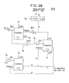
- FIG. 28 is shown in detail the construction of the address correction circuit 224 comprising three counters Cl - C3, a latching circuit LA5, an inverter I NV , an AND gate AND and OR gates OR.
- the signal SCLK is derived from the camera and in response to one clock, one picture element information is applied to the inspection device. Within the inspection device in response to the signal SCLK, the signal CLK for controlling the interior circuit components is generated.
- the signal SC L K is generated by the camera so that it is generated even when no address is generated; that is, during the time when SEND is generated to the time when SZERO is generated. However, the signal CLK is generated within the inspection device so that it is not produced between the time when the signal SZERO is produced and the time when the signal SEND is generated. It follows therefore that only the signal SCLK can be used as a timing signal for address correction.
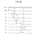
- FIG. 29 shows a timing chart of clock pulses ⁇ 1 - ⁇ 7 .
- the correct address correction may be accomplished between the time when signal SEND is produced and the time when the signal SZERO is generated.
- Each of the counters Cl - C3 is provided with a preset function.
- the preset data is derived.
- Cl is preset with the signal ST derived from the decision circuit 223 and counts the number of picture elements which are deviated.
- C2 is an up/down counter and is preset with the address at which the preceding scanning has terminated.
- C2 presets the internal address generating counter C with the address which is obtained by counting up or down the signal SCLK as the address which is most similar in phase with the present sample row datum.
- C3 produces an internal address which is an optimumly corrected scanning start address.
- the internal address consists of 16 bits. The output is used as an address for writing data into a memory or reading data therefrom.
- the clock pulses ⁇ 1 - ⁇ 7 will be described.
- the signal ST is produced.
- the data is stored into the latch LA5.
- the most significant bit of the output from the latch LA5 is applied to the up/down counter C2 as a signal representing the direction in which the sample row datum is shifted.
- the counter C2 delivers the preset data (that is, the address at which the preceding scanning has terminated).
- the clock is LOW (preset mode)
- no counting is carried out.
- the lower two bits of the output from the latching circuit LA5 are applied through the inverter INV as the preset data to the counter Cl which counts the number of picture elements which are deviated in position.
- the counter Cl counts how many picture elements in which the sample row datum deviates from the reference row datum and delivers the clock pulse ⁇ 7 .
- the signal ⁇ 4 is produced and the signal SCLK which corresponds to the number of picture elements deviated is applied to the clock input of the up/down counter C7. Therefore, the counter C2 shifts the internal address in response to the deviation so that the scanning start address may be corrected in such a way that the scanning start address is as closely in phase with the present camera scanning as possible.
- the clocks ⁇ 5 and ⁇ 6 are used to replace the corrected address with the internal address.
- FIG. 30 is shown in detail the construction of a clock generator which is adapted to generate the clocks ⁇ 1 - ⁇ 6 as shown in FIG. 29.
- the clock generator comprises D flip-flops DFl - DF5, counters C4 and C5 and inverters INV.
- the flip-flop DFl drives the counters C4 and C5 into the count mode so that the clocks ⁇ 2 and ⁇ 3 are produced.
- the clock ⁇ 3 is applied to the flip-flops DF2 and DF3 so that the clock 1 is produced.
- the clock ⁇ 1 is obtained by inverting the clock ⁇ 3 by the inverter INV.
- the output ⁇ 7 from the counter Cl is applied to the flip-flop DF4 and DF5, whereby clocks ⁇ 5 and $6 are derived.
- the reference row data are compared with the sample row data so that the inspection can be made with a higher degree of accuracy as compared with the case in which the whole reference and sample images are compared with each other.
- the circuit comprises decision elements JCl - JC7, shift registers S R l - SR6 and an overall decision circuit TJU.
- Each of the shift registers has the bits equal in number to those of the sensor array of the camera 2 (see FIG. 1).
- the reference row datum SD, decision level MD and the sample row datum TD are delayed by one picture element and applied to the decision elements JC1 - JC 7.
- the outputs from the decision elements JCl - J C7 are applied to the overall decision circuit TJU, whereby a minimum number or value is detected.
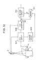
- FIG. 31 is shown a fourth embodiment of the printed image inspection device in accordance with the present invention.
- some allowance or tolerance must be provided so that a normal printed sheet may not be misjudged as spoilage. The reasons are as follows. Firstly, even a normal printed sheet has some variations in density. Secondly, the same images are not printed at the same position in a strict sense. Thirdly, noise cannot be avoided. Therefore, some suitable tolerance must be provided for the reflected-light graduation difference between the sample and reference images or picture elements.
- Tolerances vary depending upon images or their picture elements. For instance, a large degree of tolerance must be provided for a picture element adjacent to an edge of an image because the graduation difference becomes great due to the deviation caused by a printed image transport system. (see Japanese Patent Application No. 179,599/1981). Furthermore, the graduation difference due to the deviation is small at a flat portion of an image so that some tolerance must be provided in such a way that a normal printed image is misjudged as a spoilage because of variations and noise. Therefore a tolerable number of defects is determined for the total number of defective picture elements in excess of the above-described tolerance.
- the number of defective picture elements is in excess of the tolerable number of defective picture elements, a printed image is rejected, but if the number of defective picture elements is lower than the tolerable number of defective picture elements, a printed image is accepted. That is, the images are inspected based on the combination of a tolerable or allowable number of defective picture elements and the graduation difference tolerance for each picture element.
- FIG. 32 is shown the relationship between a tolerable or allowable number of defective picture elements and the graduation difference decision tolerance (%) for each picture element.
- FIG. 32 shows the following characteristics. In order to detect a spot-like stain which is caused by the scatter of ink and which has a high contrast, the decision level allowance or tolerance must be made great, but the tolerable or allowable number of defective picture elements must be made small. Furthermore, in order to detect delicate tone mismatching between the whole reference and sample prints due to the failures of color matching, the graduation difference tolerance or allowance must be made small while the tolerable or allowable number of defective picture elements must be made high. In FIG.
- the hatched area shows the area which can be inspected, but the area which is not hatched shows that a normal printed sheet is misjudged as a spoilage.
- an area at the lower right side of the characteristic curve In order to detect an ink stain, therefore, an area at the lower right side of the characteristic curve must be selected. In order to detect the color or tone mismatching, an area at the top left side of the characteristic curve must be selected.
- the camera 2 scans the printed image 1 so that the image information is derived.
- the angle of rotation of the transport cylinder 3 is detected by the rotary encoder 4, the output of which is applied to the sync circuit 307.
- the outputs from the sync circuit 307 are applied to the camera 2, an A/D converter 308 and an address circuit 309. Therefore, the scanning by the camera 2 can be synchronized; the analog-to-digital conversion of the image information derived from the camera 2 can be synchronized; and an address in an address memory 311 is accessed.
- a switch SW is inserted between the output of the A/D converter 308 on the one hand and the inputs of the memory 311 and a decision circuit 310 on the other hand.
- the output from the A/D converter 308 may be selectively applied to either the decision circuit 310 or the memory 311. More particularly, when the camera 2 is scanning a reference image 1, the movable contact of the switch SW is in the position indicated by the broken line so that the reference image information (to be referred to as “the reference data” in this specification) may be applied to the memory 311, but when the camera 2 is scanning a sample image, the movable contact of the switch SW is in the position indicated by the solid line so that the sample image information (to be referred to as "the sample data” in this specification) may be applied to the decision circuit 310 and compared with the reference data so as to find out image defects.
- T represents sample data while S, reference data.
- FIG. 33 is shown in detail the construction of the decision circuit shown in FIG. 31, comprising a number of n decision elements JEl - JEn and an OR gate OR. Both the reference and sample data S and T are applied to the decision elements JEl - JEn the outputs of which are in turn applied to the OR gate OR which in turn delivers the overall decision signal TJ.
- Each of the decision elements JEl - JEn is set with a graduation difference tolerance and a tolerable or allowable number of defective picture elements. Different graduation difference tolerances and tolerable or allowable numbers of defective picture elements are assigned to respective decision elements JEl - JEn. For instance the first decision element JEl is assigned with a relatively high graduation difference tolerance and a relatively low tolerable number of defective picture elements so that the decision element JEl can detect a spot like stain. On the other hand, the last decision element JEn is assigned with a relatively small graduation tolerance and a relatively high tolerable or allowable number of defective picture elements so that the decision element JEn can detect delicate tone differences between the whole reference and sample images.
- the decision elements JE2 - JEn-1 are assigned with graduation difference tolerances and tolerable or allowable numbers of defective picture elements between the those assigned to the first and last decision elements JEl and JEn. Therefore the decision elements JEl and JEn detect extreme image defects while the decision elements JE2 - JEn-1 detect intermediate image defects.
- the output from each of the decision elements JEl - JEn represents a spoilage and is applied to the OR gate so that the output from the OR gate represents the detection of a spoilage.
- FIG. 34 is shown in detail the construction of the decision element shown in FIG. 33.
- Sample data and reference data T and S are applied to a detector 322 (which is substantially similar in construction to that shown in FIG. 8) so that /S - T/ is derived and applied to the input terminal B of a comparator 323.
- the output E from a tolerance generator 321 is applied to the input terminal A of the comparator 323.
- the tolerance E may be generated in various ways. For instance, one tolerance may be assigned to each picture element. According to the present invention, the graduation of a picture element of the reference image is multiplied by a predetermined constant (0 - 1) and the product is a tolerance to be applied to the picture element of the sample image corresponding to the picture element of the reference image. Thus the tolerance generator 311 generates a graduation tolerance E which is obtained by multiplying reference data by a predetermined constant (0 - 1).
- the comparator 323 detects that the absolute value /S - T/ is greater than the graduation tolerance E (/S - T/ > E), it delivers an output to a counter 324. That is, the counter 324 counts the defect signals which in turn represent a number of defective picture elements.
- the output from the comparator 324 is compared with a tolerable or allowable number of defective picture elements derived from a latching circuit 326 by another comparator 325. When the number of defective picture elements (that is, the output from the counter 324) is greater than the tolerable or allowable number of defective picture elements (that is, the output from the latching circuit 326), the comparator 325 delivers a spoilage signal J .
- the tolerance generator 311 comprising a plurality of buffers B equal in number to the bits of the input signal S.
- the reference data comprise 8 bits so that eight buffers B are provided. The inputs of two of the eight buffers B are grounded and the outputs from these two buffers B are designated by MSB. The upper six bits including MSB of the sample data S are derived through the buffers B. The lowest significant bit and the next lowest significant bit of the data S are not connected so that the reference data S is shifted down by two bits and consequently the graduation tolerance E of 12.5% is obtained. In like manner, the reference data S is shifted down so that the graduation tolerance E of 50%, 25%, 6.25% or 3.125% may be obtained. In order to obtain the graduation tolerances other than described above, a multiplier such as TTL may be used.
Landscapes
- Engineering & Computer Science (AREA)
- Quality & Reliability (AREA)
- Physics & Mathematics (AREA)
- General Physics & Mathematics (AREA)
- Theoretical Computer Science (AREA)
- Computer Vision & Pattern Recognition (AREA)
- Toxicology (AREA)
- Health & Medical Sciences (AREA)
- General Health & Medical Sciences (AREA)
- Multimedia (AREA)
- Investigating Materials By The Use Of Optical Means Adapted For Particular Applications (AREA)
- Image Analysis (AREA)
- Length Measuring Devices By Optical Means (AREA)
Applications Claiming Priority (8)
| Application Number | Priority Date | Filing Date | Title |
|---|---|---|---|
| JP57151118A JPS5940241A (ja) | 1982-08-31 | 1982-08-31 | 印刷物の絵柄を検査する方法および装置 |
| JP151118/82 | 1982-08-31 | ||
| JP57185063A JPS5973758A (ja) | 1982-10-21 | 1982-10-21 | 印刷物の絵柄検査方法およびその装置 |
| JP185063/82 | 1982-10-21 | ||
| JP57208850A JPS5999592A (ja) | 1982-11-29 | 1982-11-29 | 印刷物の絵柄検査方法および装置 |
| JP208850/82 | 1982-11-29 | ||
| JP58108224A JPH0625657B2 (ja) | 1983-06-16 | 1983-06-16 | 印刷物の絵柄検査方法および装置 |
| JP108224/83 | 1983-06-16 |
Publications (3)
| Publication Number | Publication Date |
|---|---|
| EP0104477A2 true EP0104477A2 (de) | 1984-04-04 |
| EP0104477A3 EP0104477A3 (en) | 1987-01-14 |
| EP0104477B1 EP0104477B1 (de) | 1989-12-20 |
Family
ID=27469612
Family Applications (1)
| Application Number | Title | Priority Date | Filing Date |
|---|---|---|---|
| EP83108547A Expired EP0104477B1 (de) | 1982-08-31 | 1983-08-30 | Verfahren zur Bilduntersuchung |
Country Status (3)
| Country | Link |
|---|---|
| US (1) | US4677680A (de) |
| EP (1) | EP0104477B1 (de) |
| DE (1) | DE3380997D1 (de) |
Cited By (5)
| Publication number | Priority date | Publication date | Assignee | Title |
|---|---|---|---|---|
| EP0129768A3 (en) * | 1983-06-23 | 1985-09-11 | Siemens Aktiengesellschaft | Colour density measuring device |
| EP0533306A3 (en) * | 1991-09-19 | 1994-05-18 | Komori Printing Mach | Method and apparatus for recognizing meandering of web |
| DE4321177A1 (de) * | 1993-06-25 | 1995-01-05 | Heidelberger Druckmasch Ag | Vorrichtung zur parallelen Bildinspektion und Farbregelung an einem Druckprodukt |
| WO1995000337A1 (en) * | 1993-06-17 | 1995-01-05 | The Analytic Sciences Corporation | Automated system for print quality control |
| DE102005001091B3 (de) * | 2005-01-06 | 2006-04-06 | Lpcon Gmbh | Verfahren und Anordnung zur Fehlererkennung an Druckbildern während der Bahnbeobachtung von gedrucktem Material |
Families Citing this family (52)
| Publication number | Priority date | Publication date | Assignee | Title |
|---|---|---|---|---|
| US4882764A (en) * | 1985-03-29 | 1989-11-21 | Quad/Tech, Inc. | Cutoff control system |
| DE3623294A1 (de) * | 1985-07-10 | 1987-02-05 | Fuji Electric Co Ltd | System zum binaeren codieren eines bildes |
| JPH0621769B2 (ja) * | 1985-12-13 | 1994-03-23 | 大日本スクリ−ン製造株式会社 | パタ−ン欠陥検出方法およびその装置 |
| WO1988003091A1 (en) * | 1986-10-31 | 1988-05-05 | Quad/Tech, Inc. | Improved cutoff control system |
| US4847510A (en) * | 1987-12-09 | 1989-07-11 | Shell Oil Company | Method for comparison of surfaces |
| US5033378A (en) * | 1988-01-05 | 1991-07-23 | Komori Corporation | Defective print detecting device |
| JPH03223976A (ja) * | 1990-01-29 | 1991-10-02 | Ezel Inc | 画像照合装置 |
| JPH03224073A (ja) * | 1990-01-30 | 1991-10-03 | Ezel Inc | 位置合わせ装置 |
| JPH03260782A (ja) * | 1990-03-09 | 1991-11-20 | Eastman Kodak Japan Kk | パターン認識装置 |
| DE4012608A1 (de) * | 1990-04-20 | 1991-10-24 | Roland Man Druckmasch | Verfahren und vorrichtung zur bestimmung von passerdifferenzen an druckbildstellen eines mehrfarbenoffsetdruckes |
| US5144566A (en) * | 1990-06-14 | 1992-09-01 | Comar, Inc. | Method for determining the quality of print using pixel intensity level frequency distributions |
| DE4142481A1 (de) * | 1991-08-12 | 1993-02-18 | Koenig & Bauer Ag | Qualitaetskontrolle einer bildvorlage z. b. eines gedruckten musters |
| US5257325A (en) * | 1991-12-11 | 1993-10-26 | International Business Machines Corporation | Electronic parallel raster dual image registration device |
| US10361802B1 (en) | 1999-02-01 | 2019-07-23 | Blanding Hovenweep, Llc | Adaptive pattern recognition based control system and method |
| US8352400B2 (en) | 1991-12-23 | 2013-01-08 | Hoffberg Steven M | Adaptive pattern recognition based controller apparatus and method and human-factored interface therefore |
| CA2100324C (en) * | 1992-08-06 | 2004-09-28 | Christoph Eisenbarth | Method and apparatus for determining mis-registration |
| US5757981A (en) * | 1992-08-20 | 1998-05-26 | Toyo Ink Mfg. Co., Ltd. | Image inspection device |
| US5436979A (en) * | 1992-08-21 | 1995-07-25 | Eastman Kodak Company | Process for detecting and mapping dirt on the surface of a photographic element |
| DE19516354A1 (de) * | 1995-05-04 | 1996-11-07 | Heidelberger Druckmasch Ag | Verfahren zur Bildinspektion und Farbführung an Druckprodukten einer Druckmaschine |
| DE19613083A1 (de) * | 1996-04-02 | 1997-10-09 | Koenig & Bauer Albert Ag | Verfahren zur qualitativen Beurteilung von bearbeitetem Material |
| IT1306266B1 (it) | 1998-07-24 | 2001-06-04 | Gd Spa | Metodo di controllo di un oggetto stampato |
| IT1306267B1 (it) * | 1998-07-24 | 2001-06-04 | Gd Spa | Metodo e dispositivo di controllo di banconote |
| US7057732B2 (en) * | 1999-01-25 | 2006-06-06 | Amnis Corporation | Imaging platform for nanoparticle detection applied to SPR biomolecular interaction analysis |
| US8885913B2 (en) | 1999-01-25 | 2014-11-11 | Amnis Corporation | Detection of circulating tumor cells using imaging flow cytometry |
| US7450229B2 (en) * | 1999-01-25 | 2008-11-11 | Amnis Corporation | Methods for analyzing inter-cellular phenomena |
| US20060257884A1 (en) * | 2004-05-20 | 2006-11-16 | Amnis Corporation | Methods for preparing and analyzing cells having chromosomal abnormalities |
| US8131053B2 (en) | 1999-01-25 | 2012-03-06 | Amnis Corporation | Detection of circulating tumor cells using imaging flow cytometry |
| US6975400B2 (en) * | 1999-01-25 | 2005-12-13 | Amnis Corporation | Imaging and analyzing parameters of small moving objects such as cells |
| US8406498B2 (en) * | 1999-01-25 | 2013-03-26 | Amnis Corporation | Blood and cell analysis using an imaging flow cytometer |
| US7904187B2 (en) | 1999-02-01 | 2011-03-08 | Hoffberg Steven M | Internet appliance system and method |
| US8364136B2 (en) | 1999-02-01 | 2013-01-29 | Steven M Hoffberg | Mobile system, a method of operating mobile system and a non-transitory computer readable medium for a programmable control of a mobile system |
| IT1309271B1 (it) | 1999-05-27 | 2002-01-16 | Gd Spa | Metodo di controllo di banconote |
| DE19940879A1 (de) * | 1999-08-27 | 2001-03-08 | Innomess Elektronik Gmbh | Verfahren und Vorrichtung zum automatisierten Vergleich von Druckbildern an Druckmaschinen |
| US6875973B2 (en) * | 2000-08-25 | 2005-04-05 | Amnis Corporation | Auto focus for a flow imaging system |
| US6934408B2 (en) * | 2000-08-25 | 2005-08-23 | Amnis Corporation | Method and apparatus for reading reporter labeled beads |
| AU2001297843A1 (en) | 2000-10-12 | 2002-12-23 | Amnis Corporation | Imaging and analyzing parameters of small moving objects such as cells |
| CA2445960A1 (en) * | 2001-02-21 | 2002-12-19 | Amnis Corporation | Method and apparatus for labeling and analyzing cellular components |
| CA2445044C (en) * | 2001-04-25 | 2011-02-15 | Amnis Corporation | Method and apparatus for correcting crosstalk and spatial resolution for multichannel imaging |
| US6832552B2 (en) * | 2001-06-26 | 2004-12-21 | Creo Inc. | Method of automated setting of imaging and processing parameters |
| US7190832B2 (en) * | 2001-07-17 | 2007-03-13 | Amnis Corporation | Computational methods for the segmentation of images of objects from background in a flow imaging instrument |
| WO2004065544A2 (en) * | 2003-01-15 | 2004-08-05 | Amnis Corporation | Cell suspension rotating fluidic pump |
| US8307765B2 (en) * | 2004-02-06 | 2012-11-13 | Ahlstrom Corporation | Process and equipment for printing on non-woven-fabric |
| NL1025711C2 (nl) * | 2004-03-12 | 2005-09-13 | Q I Press Controls Holding B V | Werkwijze en systeem voor het controleren van door een drukpers vervaardigd drukwerk. |
| US8953866B2 (en) | 2004-03-16 | 2015-02-10 | Amnis Corporation | Method for imaging and differential analysis of cells |
| US8103080B2 (en) * | 2004-03-16 | 2012-01-24 | Amnis Corporation | Method for imaging and differential analysis of cells |
| WO2005098430A2 (en) | 2004-03-16 | 2005-10-20 | Amnis Corporation | Image based quantitation of molecular translocation |
| DE102004052181B3 (de) * | 2004-07-23 | 2006-01-19 | Koenig & Bauer Ag | Verfahren zur Erkennung eines Bahnrisses einer in einer Rollendruckmaschine bedruckten Materialbahn |
| WO2007067999A2 (en) * | 2005-12-09 | 2007-06-14 | Amnis Corporation | Extended depth of field imaging for high speed object analysis |
| US20070250008A1 (en) * | 2006-04-20 | 2007-10-25 | Gelblum Eugene A | Fluid injection apparatus and adaptor pump therefor |
| US8451524B2 (en) * | 2009-09-29 | 2013-05-28 | Amnis Corporation | Modifying the output of a laser to achieve a flat top in the laser's Gaussian beam intensity profile |
| US8817115B1 (en) | 2010-05-05 | 2014-08-26 | Amnis Corporation | Spatial alignment of image data from a multichannel detector using a reference image |
| CN109900274B (zh) * | 2019-03-25 | 2022-09-16 | 哈尔滨工业大学 | 一种图像匹配方法及系统 |
Family Cites Families (9)
| Publication number | Priority date | Publication date | Assignee | Title |
|---|---|---|---|---|
| US3944369A (en) * | 1974-05-24 | 1976-03-16 | Bell Telephone Laboratories, Incorporated | Optical comparator system to separate unacceptable defects from acceptable edge aberrations |
| US3987244A (en) * | 1975-12-31 | 1976-10-19 | United Technologies Corporation | Programmable image processor |
| US4136332A (en) * | 1976-01-30 | 1979-01-23 | Hitachi, Ltd. | Device for detecting displacement between patterns |
| US4179685A (en) * | 1976-11-08 | 1979-12-18 | Abbott Coin Counter Company, Inc. | Automatic currency identification system |
| US4197584A (en) * | 1978-10-23 | 1980-04-08 | The Perkin-Elmer Corporation | Optical inspection system for printing flaw detection |
| US4459021A (en) * | 1978-11-03 | 1984-07-10 | The Perkin-Elmer Corporation | Memory registration system |
| US4344146A (en) * | 1980-05-08 | 1982-08-10 | Chesebrough-Pond's Inc. | Video inspection system |
| DE3248928T1 (de) * | 1981-07-29 | 1983-07-07 | Dai Nippon Insatsu K.K., Tokyo | Druck-inspektionsverfahren und vorrichtung zur durchfuehrung des verfahrens |
| US4545031A (en) * | 1981-09-17 | 1985-10-01 | Kita Electrics Co., Ltd. | Photo-electric apparatus for monitoring printed papers |
-
1983
- 1983-08-30 EP EP83108547A patent/EP0104477B1/de not_active Expired
- 1983-08-30 US US06/527,947 patent/US4677680A/en not_active Expired - Lifetime
- 1983-08-30 DE DE8383108547T patent/DE3380997D1/de not_active Expired - Fee Related
Cited By (8)
| Publication number | Priority date | Publication date | Assignee | Title |
|---|---|---|---|---|
| EP0129768A3 (en) * | 1983-06-23 | 1985-09-11 | Siemens Aktiengesellschaft | Colour density measuring device |
| EP0533306A3 (en) * | 1991-09-19 | 1994-05-18 | Komori Printing Mach | Method and apparatus for recognizing meandering of web |
| US5559896A (en) * | 1991-09-19 | 1996-09-24 | Komori Corporation | Method and apparatus for recognizing meandering of web |
| WO1995000337A1 (en) * | 1993-06-17 | 1995-01-05 | The Analytic Sciences Corporation | Automated system for print quality control |
| US5712921A (en) * | 1993-06-17 | 1998-01-27 | The Analytic Sciences Corporation | Automated system for print quality control |
| DE4321177A1 (de) * | 1993-06-25 | 1995-01-05 | Heidelberger Druckmasch Ag | Vorrichtung zur parallelen Bildinspektion und Farbregelung an einem Druckprodukt |
| US5724437A (en) * | 1993-06-25 | 1998-03-03 | Heidelberger Druckmaschinen Ag | Device for parallel image inspection and inking control on a printed product |
| DE102005001091B3 (de) * | 2005-01-06 | 2006-04-06 | Lpcon Gmbh | Verfahren und Anordnung zur Fehlererkennung an Druckbildern während der Bahnbeobachtung von gedrucktem Material |
Also Published As
| Publication number | Publication date |
|---|---|
| US4677680A (en) | 1987-06-30 |
| EP0104477A3 (en) | 1987-01-14 |
| DE3380997D1 (de) | 1990-01-25 |
| EP0104477B1 (de) | 1989-12-20 |
Similar Documents
| Publication | Publication Date | Title |
|---|---|---|
| US4677680A (en) | Method and device for inspecting image | |
| EP0467149B1 (de) | Verfahren und Vorrichtung zur Prüfung eines Musters einer gedruckten Leiterplatte | |
| US4806780A (en) | Image correction method and apparatus with partial detector array sampling | |
| US4668982A (en) | Misregistration/distortion correction scheme | |
| US6317512B1 (en) | Pattern checking method and checking apparatus | |
| US5293430A (en) | Automatic image segmentation using local area maximum and minimum image signals | |
| US4707734A (en) | Coarse flaw detector for printed circuit board inspection | |
| US4578810A (en) | System for printed circuit board defect detection | |
| US4197584A (en) | Optical inspection system for printing flaw detection | |
| US4791586A (en) | Method of and apparatus for checking geometry of multi-layer patterns for IC structures | |
| US4131879A (en) | Method and apparatus for determining the relative positions of corresponding points or zones of a sample and an orginal | |
| US4242702A (en) | Apparatus for automatically checking external appearance of object | |
| EP0466013B1 (de) | Verfahren und Vorrichtung zur Musterprüfung gedrukter Schaltungsplatten | |
| EP0217414B1 (de) | Verfahren und Vorrichtung zur Mustermaskierung | |
| US4442542A (en) | Preprocessing circuitry apparatus for digital data | |
| US5185811A (en) | Automated visual inspection of electronic component leads prior to placement | |
| US5200841A (en) | Apparatus for binarizing images | |
| US5440650A (en) | Image processing system for inspection of overprinted matter | |
| EP0468371B1 (de) | Verfahren und Gerät zur Kompensation von Lese-Positionsfehlern eines Bildsensors | |
| US4349880A (en) | Inspection system for detecting defects in regular patterns | |
| US7142238B1 (en) | Image pick-up device | |
| US5912985A (en) | Pattern detection method | |
| EP0311990B1 (de) | Verfahren und Vorrichtung zum Nachweis von Ungleichheiten in der zyklischen Länge von gedruckten Mustern | |
| JP2696000B2 (ja) | プリント基板のパターン検査方法 | |
| JP3204876B2 (ja) | 印刷物検査装置 |
Legal Events
| Date | Code | Title | Description |
|---|---|---|---|
| PUAI | Public reference made under article 153(3) epc to a published international application that has entered the european phase |
Free format text: ORIGINAL CODE: 0009012 |
|
| AK | Designated contracting states |
Designated state(s): DE GB |
|
| RAP1 | Party data changed (applicant data changed or rights of an application transferred) |
Owner name: DAI NIPPON INSATSU KABUSHIKI KAISHA |
|
| PUAL | Search report despatched |
Free format text: ORIGINAL CODE: 0009013 |
|
| AK | Designated contracting states |
Kind code of ref document: A3 Designated state(s): DE GB |
|
| 17P | Request for examination filed |
Effective date: 19870415 |
|
| 17Q | First examination report despatched |
Effective date: 19880620 |
|
| GRAA | (expected) grant |
Free format text: ORIGINAL CODE: 0009210 |
|
| AK | Designated contracting states |
Kind code of ref document: B1 Designated state(s): DE GB |
|
| REF | Corresponds to: |
Ref document number: 3380997 Country of ref document: DE Date of ref document: 19900125 |
|
| PLBI | Opposition filed |
Free format text: ORIGINAL CODE: 0009260 |
|
| 26 | Opposition filed |
Opponent name: GAO GESELLSCHAFT FUER AUTOMATION UND ORGANISATION Effective date: 19900920 |
|
| PLAB | Opposition data, opponent's data or that of the opponent's representative modified |
Free format text: ORIGINAL CODE: 0009299OPPO |
|
| R26 | Opposition filed (corrected) |
Opponent name: GAO GESELLSCHAFT FUER AUTOMATION UND ORGANISATION Effective date: 19900920 |
|
| PLBN | Opposition rejected |
Free format text: ORIGINAL CODE: 0009273 |
|
| STAA | Information on the status of an ep patent application or granted ep patent |
Free format text: STATUS: OPPOSITION REJECTED |
|
| 27O | Opposition rejected |
Effective date: 19940711 |
|
| PGFP | Annual fee paid to national office [announced via postgrant information from national office to epo] |
Ref country code: DE Payment date: 20010820 Year of fee payment: 19 |
|
| PGFP | Annual fee paid to national office [announced via postgrant information from national office to epo] |
Ref country code: GB Payment date: 20010830 Year of fee payment: 19 |
|
| REG | Reference to a national code |
Ref country code: GB Ref legal event code: IF02 |
|
| PG25 | Lapsed in a contracting state [announced via postgrant information from national office to epo] |
Ref country code: GB Free format text: LAPSE BECAUSE OF NON-PAYMENT OF DUE FEES Effective date: 20020830 |
|
| PG25 | Lapsed in a contracting state [announced via postgrant information from national office to epo] |
Ref country code: DE Free format text: LAPSE BECAUSE OF NON-PAYMENT OF DUE FEES Effective date: 20030301 |
|
| GBPC | Gb: european patent ceased through non-payment of renewal fee |
Effective date: 20020830 |
|
| APAH | Appeal reference modified |
Free format text: ORIGINAL CODE: EPIDOSCREFNO |