EP0102614A2 - Verfahren und Gerät zur Regelung eines pulsbreitenmodulierten Wechselrichters - Google Patents
Verfahren und Gerät zur Regelung eines pulsbreitenmodulierten Wechselrichters Download PDFInfo
- Publication number
- EP0102614A2 EP0102614A2 EP83108555A EP83108555A EP0102614A2 EP 0102614 A2 EP0102614 A2 EP 0102614A2 EP 83108555 A EP83108555 A EP 83108555A EP 83108555 A EP83108555 A EP 83108555A EP 0102614 A2 EP0102614 A2 EP 0102614A2
- Authority
- EP
- European Patent Office
- Prior art keywords
- signal
- pwm inverter
- pwm
- current
- signals
- Prior art date
- Legal status (The legal status is an assumption and is not a legal conclusion. Google has not performed a legal analysis and makes no representation as to the accuracy of the status listed.)
- Granted
Links
Images


Classifications
-
- H—ELECTRICITY
- H02—GENERATION; CONVERSION OR DISTRIBUTION OF ELECTRIC POWER
- H02M—APPARATUS FOR CONVERSION BETWEEN AC AND AC, BETWEEN AC AND DC, OR BETWEEN DC AND DC, AND FOR USE WITH MAINS OR SIMILAR POWER SUPPLY SYSTEMS; CONVERSION OF DC OR AC INPUT POWER INTO SURGE OUTPUT POWER; CONTROL OR REGULATION THEREOF
- H02M7/00—Conversion of ac power input into dc power output; Conversion of dc power input into ac power output
- H02M7/42—Conversion of dc power input into ac power output without possibility of reversal
- H02M7/44—Conversion of dc power input into ac power output without possibility of reversal by static converters
- H02M7/48—Conversion of dc power input into ac power output without possibility of reversal by static converters using discharge tubes with control electrode or semiconductor devices with control electrode
- H02M7/505—Conversion of dc power input into ac power output without possibility of reversal by static converters using discharge tubes with control electrode or semiconductor devices with control electrode using devices of a thyratron or thyristor type requiring extinguishing means
- H02M7/515—Conversion of dc power input into ac power output without possibility of reversal by static converters using discharge tubes with control electrode or semiconductor devices with control electrode using devices of a thyratron or thyristor type requiring extinguishing means using semiconductor devices only
- H02M7/525—Conversion of dc power input into ac power output without possibility of reversal by static converters using discharge tubes with control electrode or semiconductor devices with control electrode using devices of a thyratron or thyristor type requiring extinguishing means using semiconductor devices only with automatic control of output waveform or frequency
- H02M7/527—Conversion of dc power input into ac power output without possibility of reversal by static converters using discharge tubes with control electrode or semiconductor devices with control electrode using devices of a thyratron or thyristor type requiring extinguishing means using semiconductor devices only with automatic control of output waveform or frequency by pulse width modulation
-
- H—ELECTRICITY
- H02—GENERATION; CONVERSION OR DISTRIBUTION OF ELECTRIC POWER
- H02M—APPARATUS FOR CONVERSION BETWEEN AC AND AC, BETWEEN AC AND DC, OR BETWEEN DC AND DC, AND FOR USE WITH MAINS OR SIMILAR POWER SUPPLY SYSTEMS; CONVERSION OF DC OR AC INPUT POWER INTO SURGE OUTPUT POWER; CONTROL OR REGULATION THEREOF
- H02M7/00—Conversion of ac power input into dc power output; Conversion of dc power input into ac power output
- H02M7/42—Conversion of dc power input into ac power output without possibility of reversal
- H02M7/44—Conversion of dc power input into ac power output without possibility of reversal by static converters
- H02M7/48—Conversion of dc power input into ac power output without possibility of reversal by static converters using discharge tubes with control electrode or semiconductor devices with control electrode
Definitions
- This invention relates to a method and apparatus for controlling a PWM (pulse width modulation) inverter, in which higher harmonic components included in the output currents of the PWM inverter driving an AC motor are reduced so as to reduce magnetic noise (acoustic noise) generated from the AC motor.
- PWM pulse width modulation
- An instantaneous-value control system and a mean-value control system are generally used for the control of a PWM inverter.
- turn-on control of the PWM inverter is made by PWM pulse which is modulated on the basis of differences of magnitude and polarity between a current command pattern signal (a sinusoidal wave signal), and a detected current signal at the inverter output.
- This instantaneous-value control system is advantageous over the mean-value control system.
- a voltage command pattern signal is used as a modulation signal and is compared with a carrier wave signal (a triangular wave signal) to generate a PWM pulse signal for each phase.
- the current control response of the former system is better than that of the latter system.
- the former proposal is defective in that magnetic noise cannot-be reduced in the rated-load operating condition of the motor when the magnetic flux density attains its rating, although such magnetic noise can successfully be reduced in the no-loaded (or light-loaded) operating condition of the motor: Also, the latter proposal is defective in that the current control response is lowered in the operation range (the low-speed operation range) controlled by the mean-value control system, and that a torque variation occurs at the time of switch- over between the control systems.
- a method for controlling a PWM inverter which drives an AC motor and which is turned on under control of pulse width modulation means comparing a detected current signal with a current command pattern signal for each of the individual phases to find a current error in each phase, and, on the basis of the magnitude and polarity of the current error, generating a PWM pulse signal for each phase, the method comprising applying an AC signal from signal generating means to the pulse width modulation means so that the PWM pulse signals generated from the pulse width modulation means act to increase the effective value of the neutral voltage of the output of the PWM inverter.
- a PWM inverter control apparatus comprising a PWM inverter driving an AC motor, current command means generating current command pattern signals for commanding output currents of the PWM inverter in the individual phases, current detection means detecting the output currents of the PWM inverter, pulse width modulation means for generating PWM pulse signals based on the magnitude and polarity of current errors between the current command pattern signals and the detected current signals of the individual phases, and signal generating means for generating an AC signal and applying it to the pulse width modulation means so that the PWM pulse signals generated from the pulse width modulation means act to increase the effective value of the neutral voltage of the output of the PWM inverter.
- an AC voltage applied from a commercial AC power source AC is converted into a DC voltage by a diode rectifier circuit 1.
- the DC voltage from the rectifier circuit 1 is applied to a PWM inverter 3 after being smoothed by a smoothing capacitor 2.
- the PWM inverter 3 includes self-extinguish elements S up , S , ..., S WN of G raetz connection and feedback diodes D u p, D VP , ..., D WN connected in inverse-parallel relation to the associated self-extinguish elements respectively.
- These self-extinguish elements are switching'elements such as gate turn-off thyristors or transistors.
- An induction motor 4 is connected at its input terminals to the U-phase, V-phase and W-phase AC output terminals of the PWM inverter 3.
- a speed detector 5 is mechanically coupled to the induction motor 4.
- the U-phase and V-phase primary currents i U and i V (the output currents of the inverter 3) supplied to the induction motor 4 are detected by current detectors 8U and 8V respectively.
- Signals indicative of the currents i U and i V detected by the current detectors 8U and 8V are applied in illustrated polarity to adders 9U and 9V respectively and are also applied in illustrated polarity to another adder 9W which generates a signal indicative of the detected W-phase primary current i w of the induction motor 4.
- a speed command signal N from a speed command circuit 13 and a detected speed signal N from the speed detector 5 are compared in illustrated polarities in a comparator 14, and the comparator output signal indicative of the speed error AN is amplified by a speed error amplifier 15.
- the output signal from the speed error amplifier 15 is applied as a torque command signal ⁇ to a current command circuit 6 and to an adder 16.
- a voltage-frequency (V-F) converter 17 generates a frequency command signal f 1 proportional to the sum of the rotation frequency proportional to the detected speed signal N and the slip frequency proportional to the torque command signal ⁇ .
- the frequency command signal f 1 determines the output frequency of the PWM inverter 3 (the primary frequency of the induction motor 4).
- the current command circuit 6 generates current command pattern signals i U and i V which have an amplitude proportional to the value of the * torque command signal ⁇ , a frequency proportional to the value of the frequency command signal f 1 * and a phase difference of 120°.
- the current command pattern signals i U and i v are applied to comparators 10U and 10V having a hysteresis characteristic respectively.
- these two current command * * signals i u and i v are added in illustrated polarity in an adder 7 to be subjected to vector addition.
- the adder 7 generates a W-phase current command pattern signal i W which is applied to a comparator 10W having a hysteresis characteristic.
- a signal generator 12 generates an AC signal e c of triangular waveform which is applied in illustrated polarity to the adders 9U, 9V and 9W.
- the comparators 10U, 10V and 10W compare the output signals i OU , i OV and i OW .from the adders 9U, 9V and 9W with the current command pattern signals i U * , i V * and i W * respectively and generate pulse width modulation (PWM) pulse signals P U , P v and P W for turning on/off the switching elements S UP , S VP , ..., S WN constituting the PWM inverter 3.
- PWM pulse width modulation
- gate circuits 11U, 11V and 11W apply gate signals to the switching elements SUP, S VP , ..., S WN .
- the output currents i U , i v and i W of the PWM inverter 3 have a positive polarity when they flow in the direction shown by the arrows in Fig. 1.
- the currents i U , i v and i w increase in the positive direction when the switching elements SUP, S VP and S WP are turned on, but increase in the negative direction when the switching elements S UN , S VN and S WN are turned on.
- the currents i U , i v and i W of positive polarity decrease by flowing through the diodes D UN ' D VN and D WN when the switching elements S UP , S VP and S WP are turned off respectively
- the currents i U , i v and i W of negative polarity decrease by flowing through the diodes D UP , DV p and D WN when the-switching elements S UN' S VN and S WN are turned off respectively.
- the switching elements S UP , S VP , ..., S WN are turned on/off by the PWM pulse signals P U' P v and P W generated from the comparators 10U, 10V and 10W.
- the relation between the current command pattern signal i U and the detected current signal i u (the output signal i OU of the adder 9U) applied to the comparator 10U is shown in Fig. 2(a).
- the PWM pulse signal P U of "1" level appears from the comparator 10U as shown in Fig. 2(e).
- the gate circuit llU applies the gate signal to the switching element S UP . Since the polarity of the U-phase current i U in the period T 1 is positive, the U-phase current i U increases when the switching element S UP is turned on.
- the polarity of the U-phase current i U in the period T 1 is positive. Therefore, when the switching element S UP is turned off, the U-phase current i U decreases by flowing through the diode D UN . When the U-phase current i U decreases until its level becomes lower than the current command pattern signal i U by the hysteresis deviation - ⁇ I, the PWM pulse signal P U of "1" level is generated from the comparator 10U again, and the aforementioned operation is repeated. The U-phase current i U flows through the switching element S UN and diode D UP when the polarity of this current i U is negative.
- the U-phase current i U of the PWM inverter 3 is controlled to follow the pattern provided by the current command pattern signal i U . It is apparent that the V-phase current i V and W-phase current i w of the PWM inverter 3 are also similarly controlled by the PWM pulse signals P v and P W generated from the respective comparators 10V and 10W.
- the relation between the V-phase current command pattern signal i V and the V-phase current i V is shown in Fig. 2(b), and the PWM pulse signal P V generated from the comparator 10V is shown in Fig. 2(f).
- the relation between the W-phase current command pattern signal i W and the W-phase current i w is shown in Fig. 2(c), and the PWM pulse signal P W generated from the comparator 10W is shown in Fig. 2(g).
- the instantaneous-value control of the PWM inverter 3 is carried out in the manner above described. That is, the instantaneous-value control of the PWM inverter 3 is such that the instantaneous values of the output currents i U , i V and i w are detected and compared with the current command pattern signals i U , i v and i W respectively for switching the required switching elements in the PWM inverter 3 depending on the results of comparison.
- the output currents i U , i V and i W of the PWM inverter 3 can be controlled with a high response.
- the PWM inverter 3 Since the PWM inverter 3 is on-off controlled by the PWM pulse signals P U , P V and P W in the manner above described, its output voltages (phase voltages) change in synchronism with the PWM pulse signals P U , P V and P W .
- Line voltages e u-v '. e v-w and e w-u corresponding to the differences between the U-phase voltage e U , V-phase voltage e V and W-phase voltage e W in the period T 1 shown in Fig. 2 are as shown in Figs. 3(i), 3(j) and 3(k) respectively.
- each of the line voltages shown in Figs. 3(i), 3(j) and 3(k) changes in the positive and negative directions with a period shorter than that of the fundamental wave in the period T l , many higher harmonic voltage components are included in these line voltages. Therefore, many higher harmonic current components flow to the induction motor 4 to increase the amount of magnetic noise.
- the triangular wave signal e C having a waveform as shown in Fig. 2(d) is added to the detected current signals i U , i V and i W in the adders 9 U , 9 V and 9W respectively.
- the signals i OU , i OV and i OW obtained by addition of the triangular wave signal e C to the detected current signals i U , i v and i W are applied from the adders 9U, 9V and 9W to the comparators 10U, 10V and 10W to be compared with the current command pattern signals i U * , i V * and i W respectively.
- the comparators 10U, 10V and 10W act to turn the PWM pulse signals p U , P V and P W from the "1" level to the "-1" level when the following relation holds:
- the PWM pulse signals P U , P V and P w are turned from the "-1" level to the "1” level when the following relation holds:
- the comparators 10U, 10V and 10W generate such PWM pulse signals P U , P v and P W on the basis of the magnitude and polarity of current errors ⁇ i U , ⁇ i V and ⁇ i W between the current command pattern signals i U *, i V * , i W and the sum signals i OU . i OV' i OW respectively.
- addition of the triangular wave signal e c to the detected current signals i U , i v and i w is equivalent to changing of the hysteresis deviations ⁇ I of the comparators 10U, 10V and 10W by the triangular wave signal e C .
- the waveforms representing the results of addition of the triangular wave signal e C to the current command pattern signals i U *, i V * and i W * are quite complex when illustrated. In the period T 2 in Fig. 2, therefore, the waveforms representing the changed hysteresis deviations ⁇ I are merely shown to avoid complexity.
- the voltage e N at the neutral point has a -waveform as shown in Fig. 2(h). It will be seen in Fig. 2(h) that the effective value of the neutral voltage e N in the period T 2 is larger than that in the period T 1 .
- the triangular wave signal e C is added to the detected current signals i U , i v and i w in a relation which increases the effective value of the neutral voltage e N .
- the PWM pulse signals P U , P v and P W applied to the PWM inverter 3 act to increase the effective value of the neutral voltage e N .
- Fig. 4 shows another embodiment of the present invention in which an AC signal (a rectangular wave signal) is superposed on current command pattern signals.
- a signal generator 20 generates an AC signal e S of rectangular waveform which is applied to adders 21U, 21V and 21 W .
- Current command pattern signals i U , i V and i w from the current command circuit 6 are applied in positive polarity to the adders 21U and 21V respectively and are also applied in negative polarity to the adder 21W.
- the adder 21W generates a W-phase current command pattern signal i w which * * represents the vector sum of the signals i U and i V .
- Detected current signals i U and i V from the respective current detectors 8U and 8V are applied to an adder 22, and a W-phase detected current signal i w representative of the vector sum of the signals i U and i v is generated from the adder 22.
- Fig. 5(a) shows the detected current signal i U and a sum signal i PU applied as inputs to the comparator 10U.
- the sum signal i PU is representative of the sum of the current command pattern signal i U and the rectangular wave signal e s having a waveform as shown in Fig. 5(d).
- the comparator 10U generates a PWM pulse signal P U having a waveform as shown in Fig. 5(e).
- the polarity of the PWM pulse signal P U generated from the comparator 10U is inverted when the error ⁇ i U of the detected current signal i U relative to the sum signal i PU applied from the adder 21U exceeds the hysteresis deviation + ⁇ I or -AI of the comparator 10U.
- the one-dot chain curves in Fig. 5(a) represent the hysteresis deviations ⁇ AI of the comparator 10U.
- the rectangular wave signal e S is not added to or superposed on the current command pattern signal i U * .
- the comparators 10V and 10W operate also in a manner similar to the comparator 10U and generate PWM pulse signals P V and P W having waveforms as shown in Figs. 5(f) and 5(g) respectively.
- the rectangular wave signal e S is applied to the adders 21U, 21V and 21 W .
- the PWM pulse signals P U , P V and P W generated from the comparators 10U, 10V and 10W have waveforms as shown in Figs. 5(e), 5(f) and 5(g) respectively.
- the U-V line voltage e u-v has a waveform as shown in Fig. 5(h). It will be seen in Fig. 5(h) that the effective value of the line voltage e U-V in the period T 2 is smaller than that in the period T 1 in which the rectangular wave signal e S is not added, and the higher harmonic voltage components are correspondingly decreased.
- Fig. 4 is as effective as the embodiment shown in Fig. 1 in that the higher harmonic currents can be decreased to reduce undesirable magnetic noise.
- Fig. 5(i) shows the waveform of the neutral voltage e N in the embodiment shown in Fig. 4.
- the function of this second embodiment is the same as that of the first embodiment shown in Fig. 1 in that the rectangular wave signal e s , in lieu of the triangular wave signal e C' is added to the current command pattern signals i U *, i V * and i w * so that the PWM pulse signals P U , P V and P W applied to the PWM inverter 3 act to increase the effective value of the neutral voltage e N of the inverter output voltages.
- Fig. 6 shows still another embodiment of the present invention in which a triangular wave signal is applied to comparators so as to change the hysteresis deviations of the comparators.
- a hysteresis deviation adjusting circuit 23 adjusts the hysteresis deviations ⁇ I of the comparators 10U, 10V and 10W in response to the application of a triangular wave signal e C generated from the signal generator 12.
- Fig. 7 shows in detail the structure of the comparator 10U and hysteresis deviation adjusting circuit 23.
- a current command pattern signal i U * and a detected current signal i U are applied through respective resistors 36 and 37 to the inverted input negative terminal of a comparing amplifier 35 in the comparator 10U.
- the output voltage of the comparing amplifier 35 is divided by resistors 38 and 39, and such a divided voltage signal is applied to the non-inverted input positive terminal of the comparing amplifier 35.
- the resistance values of these resistors 38 and 39 determine the hysteresis deviations ⁇ I of the comparator 10U.
- Diodes 40 and 41 are provided for limiting the output voltage of the comparing amplifier 35, and the voltage limit can be adjusted by associated resistors 42 and 43.
- the parts 35 to 43 described above constitute the comparator 10U.
- the hysteresis deviation adjusting circuit 23 includes a limit command circuit 30 which commands the standard limit IS of the output voltage of the comparing amplifier 35.
- the signal indicative of the standard limit IS is applied in illustrated polarity to adders 31 and 32 to be added to the triangular wave signal e C applied in illustrated polarity to the adders 31 and 32, and the output signals from the adders 31 and 32 are amplified by amplifiers 33 and 34 respectively.
- the output signals from the amplifiers 33 and 34 are applied to the associated terminals of the resistors 42 and 43 respectively.
- the output signals from the amplifiers 33 and 34 are applied also to the comparators 10V and 10W.
- the divided voltage signal provided by dividing the output voltage of the comparing amplifier 35 by the resistors 38 and 39 is fed back to the non-inverted input positive terminal of the comparing amplifier 35, so that the comparing amplifier 35 operates with a hysteresis characteristic.
- the hysteresis deviations ⁇ AI can be adjusted by the level of the voltage signal fed back to the non-inverted input positive terminal of the comparing amplifier 35, and the level of the feedback voltage can be changed by the amplitude of the output voltage of the comparing amplifier 35.
- the diodes 40, 41 and the resistors 42, 43 constitute a known limiter circuit so that the limit is variable depending on the levels of the output voltages of the amplifiers 33 and 34.
- the diode 41 is turned on when the comparing amplifier 3.5 generates a negative voltage which exceeds a predetermined value in relation to the output voltage of the amplifier 34 applied through the resistor 43. Consequently, the absolute value of the output voltage (negative) of the comparing amplifier 35 decreases, and the output voltage of the comparing amplifier 35 is limited to a value corresponding to the output voltage of the amplifier 34. Similarly, the positive output voltage of the comparing amplifier 35 is limited by the function of the diode 40 to a value corresponding to the output voltage of the amplifier 33.
- the output voltages of the amplifiers 33 and 34 have constant values proportional to the standard limit IS. Therefore, the hysteresis deviations ⁇ I of the comparing amplifier 35 are also constant.
- the output voltages of the amplifiers 33 and 34 change in synchronism with the triangular wave signal e C . Since the output voltage of the comparing amplifier 35 is limited by the output voltages of the amplifiers 33 and 34, the hysteresis deviations ⁇ I change in synchronism with the triangular wave signal e C .
- the line voltages can be decreased to reduce undesirable magnetic noise generated from the induction motor 4, as in the case.of the embodiment shown in Fig. 1.
- Fig. 8 shows yet another embodiment of the present invention in which a voltage signal indicative of the voltage at the neutral point of the primary windings of an induction motor is added to current command pattern signals i U *, i V * and i w *.
- a speed control circuit 45 includes the combination of the current command circuit 6, the comparator 14, the speed error amplifier 15, the adder 16 and the V-F converter 17 shown in Fig. 1.
- a neutral voltage detection circuit 46 generates a neutral voltage signal e N which represents the sum of PWM pulse signals P U , P v and P w applied from the comparators 10U, 10V and 10W thereto in illustrated polarity and which is applied to the adders 21U, 21V and 21W in illustrated polarity.
- Figs. 9 and 10 show operating waveforms of the embodiment shown in Fig. 8.
- the signals shown in Figs. 9(d) to 9(g) are the same as those shown in Figs. 10(d) to 10(g) respectively.
- the neutral voltage signal e N is not applied to the adders 21U, 21V and 21W from the neutral voltage detection circuit 46, while, in another period T 2 , the signal e N is applied to the adders 21U, 21V and 21W.
- Figs. 9(a), 9(b) and 9(c) show the relation between current command pattern signals i U *, i V * and i W * and U-phase, V-phase and W-phase detected current signals i U , i v and i W respectively.
- Figs. 9(d), 9(e) and 9(f) show the waveforms of the PWM pulse signals P U , P V and P W generated from the comparators 10U, 10V and 10W respectively.
- the PWM inverter 3 is on-off controlled by the PWM pulse signals P U , P v and P W applied through the gate circuits 11U, 11V and 11W from the comparators 10U, 10V and 10W respectively, and, in this case, the voltage signal e N indicative of the voltage at the neutral point of the primary windings of the induction motor 4 has a waveform as shown in Fig. 9(g). Also, line voltages e U - V' e V-W and e W-U have waveforms as shown in Figs. 10 (h) , 10(i) and 10(j) respectively.
- Fig. 8 The operation of the embodiment shown in Fig. 8 is similar to that of the embodiment shown in Fig. 1.
- the neutral voltage signal e N is added to the current command pattern signals i U * , i V * and i W * in Fig. 8,
- Figs. 9(a), 9(b) and 9(c) illustrate that the hysteresis deviations ⁇ AI of the comparators 10U, 10V and 10W are changed by application of the signal e N .
- the neutral voltage signal e N is added to the current command pattern signals i U *, i V * and i W * in the embodiment of Fig. 8 so that the PWM pulse signals P U , PV and P W applied to the PWM inverter 3 act to increase the effective value of the neutral voltage e N , as in the case of the embodiment shown in Fig. 1.
- the neutral voltage signal e N * is added to the current command pattern signals i in the embodiment shown in Fig. 8, the operation is also the same when the signal e N is added to the detected current signals i in the same polarity. Also, the hysteresis deviations ⁇ I of the comparators 10U, 10V and 10W may be directly changed by application of the neutral voltage signal e N , as in the case of the embodiment shown in Fig. 6. This is readily apparent from the expressions (1) and (2).
- the neutral voltage signal e N is provided by the sum of the U-phase, V -phase and W-phase PWM pulse signals P U , P v and P w in the embodiment of Fig. 8, it is apparent that it may be provided by the sum of the detected U-phase, V-phase and W-phase output voltages of the P W M inverter 3 or it may be detected from the neutral point of the primary windings of the induction motor 4.
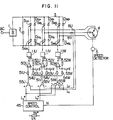
- Fig. 11 shows a further embodiment of the present invention in which the neutral voltage signal e N is applied directly to the positive input terminals of comparing amplifiers constituting the individual comparators 10U, 10V and 10W.
- adders 55U, 55V and 55W generate output signals indicative of U-phase, V-phase and W-phase current errors ⁇ i V , ⁇ i V and ⁇ i W respectively in response to the application of current command pattern signals i U *, i V * and detected current signals i U , i V .
- the signals indicative of the U-phase, V-phase and W-phase current errors ⁇ i U , ⁇ i V and ⁇ i W are applied through input resistors 51U, 51V and 51W to the negative input terminals of comparing amplifiers 50U, 50V and 50W respectively.
- PWM pulse signals P U , P vand P W (proportional to phase voltages e U , e v and e W ) generated from the comparing amplifiers 50U, 50V and 50W are voltage-divided by feedback resistors 52U, 53U; 52V, 53V; and 52W, 53W, and such divided voltage signals are fed back to the positive input terminals of the comparing amplifiers 50U, 50V and 50W respectively.
- the comparing amplifiers 50 and the resistors 51, 52, 53 constitute the comparators 10 having the hysteresis characteristic.
- the hysteresis deviations ⁇ I of each of these comparators 10 are determined by the ratio between the resistance values of the associated resistors 52 and 53.
- the hysteresis deviations ⁇ I of each of the comparators 10 become larger with the increase of the feedback voltage applied to its positive input terminal.
- the positive input terminals of the U-phase, V-phase and W-phase comparing amplifiers 50U, 50V and 50W are interconnected through resistors 54U, 54V and 54W respectively.
- the first term in the parentheses on the right-hand side of the equation (3) represents the value of the output voltage signal e 0 of the comparing amplifier 50
- the second term represents the value of the neutral voltage signal e N
- the output voltage signal e 0 of the comparing amplifier 50 is a binary signal having either a positive polarity or a negative polarity, and the application of such a signal e o to the positive input terminal of the comparing amplifier 50 provides the hysteresis characteristic.
- the embodiment of Fig. 11 operates in a manner similar to that of the embodiment of Fig. 8 to exhibit the effect of magnetic noise reduction.
- the positive input terminals of the comparing amplifiers 50U, 50V and 50W are interconnected through the resistors 54U, 54V and 54W.
- the positive input terminals of the comparing amplifiers 50U, 50V and 50W may be directly interconnected to exhibit substantially the same effect.
- the feedback voltage e f applied to the positive input terminal of the comparing amplifier 50 is expressed as follows:
- the feedback voltage e f given by the equation (4) is proportional to the neutral voltage e N only, and the hysteresis characteristic provided in relation to the voltage e 0 disappears.
- the comparing amplifiers 50U, 50V and 50 W can satisfactorily operate to generate the required PWM pulse signals P U , P V and P W . This arrangement can achieve the desired function without increasing the number of resistors.
- an AC signal such as a triangular wave signal, a rectangular wave signal, a sinusoidal wave signal or a neutral voltage signal is applied in common to U-phase, V-phase and W-phase comparators a hysteresis characteristic and which have generate PWM pulse signals for the purpose of turn-on control of a PWM inverter, so that these PWM pulse signals act to increase the effective value of the neutral voltage thereby reducing undesirable magnetic noise.
- Figs. 12 to 14 are graphs showing experimental results for illustrating the effect of the present invention.
- An induction motor having a capacity of 5.5 kW was used in the experiments.
- Fig. 12 is a graph showing the relation between the rotation speed of the induction motor and noise when an AC signal of 200 Hz was applied.
- the broken line a in Fig. 12 represents the level of background noise, and the curve b represents the relation between the motor rotation speed and noise in the absence of the AC signal.
- the curves c, d and e represent the same relations when a triangular wave signal, a sinusoidal wave signal and a rectangular wave signal are applied as the AC signal respectively. It will be apparent from Fig. 12 that the noise level is generally reduced by application of the AC signal and, especially, the noise level can be greatly reduced at low rotation speeds of the induction motor.
- Figs. 13 and 14 are-graphs showing the relation between the voltage of the AC signal and noise when a rectangular wave signal was applied as the AC signal and its frequency was set at 50 Hz, 200 Hz and 500 Hz.
- the rotation speed of the induction motor is 0 rpm
- the rotation speed is 50 rpm. It will be seen from Figs. 13 and 14 that the higher the voltage of the applied AC signal, the lower is the noise level, and the lower the frequency of the applied AC signal, the greater is the effect of noise reduction when the AC voltage is the same.
- an AC signal is applied in common to U-phase, V-phase and W-phase comparators which have a hysteresis characteristic and generate PWM pulse signals for the purpose of turn-on control of a PWM inverter, so that these PWM pulse signals act to increase the effective value of the neutral voltage of the PWM inverter output voltages, whereby magnetic noise generated from an AC motor driven by the PWM inverter can be reduced regardless of the load, and the desired current control with a high response can be achieved.
- the AC signal may be applied to the U-phase, V-phase and W-phase comparators only when the induction motor rotates at low speeds where generation of magnetic noise therefrom is not ignorable.
Landscapes
- Engineering & Computer Science (AREA)
- Power Engineering (AREA)
- Inverter Devices (AREA)
- Control Of Ac Motors In General (AREA)
Applications Claiming Priority (2)
| Application Number | Priority Date | Filing Date | Title |
|---|---|---|---|
| JP152622/82 | 1982-09-03 | ||
| JP57152622A JPS5944975A (ja) | 1982-09-03 | 1982-09-03 | Pwmインバ−タの制御方法および装置 |
Publications (3)
| Publication Number | Publication Date |
|---|---|
| EP0102614A2 true EP0102614A2 (de) | 1984-03-14 |
| EP0102614A3 EP0102614A3 (en) | 1984-12-27 |
| EP0102614B1 EP0102614B1 (de) | 1987-07-15 |
Family
ID=15544398
Family Applications (1)
| Application Number | Title | Priority Date | Filing Date |
|---|---|---|---|
| EP83108555A Expired EP0102614B1 (de) | 1982-09-03 | 1983-08-30 | Verfahren und Gerät zur Regelung eines pulsbreitenmodulierten Wechselrichters |
Country Status (4)
| Country | Link |
|---|---|
| US (1) | US4629959A (de) |
| EP (1) | EP0102614B1 (de) |
| JP (1) | JPS5944975A (de) |
| DE (1) | DE3372560D1 (de) |
Cited By (11)
| Publication number | Priority date | Publication date | Assignee | Title |
|---|---|---|---|---|
| DE3231945A1 (de) * | 1982-08-11 | 1984-02-16 | Bbc Brown Boveri & Cie | Zweipulsiger wechselrichter mit einer vorrichtung zur toleranzbandsteuerung |
| EP0117558A2 (de) * | 1983-02-28 | 1984-09-05 | Hitachi, Ltd. | Verfahren und Gerät zur Regelung eines pulsbreitenmodulierten Wechselrichters |
| GB2187312A (en) * | 1986-02-06 | 1987-09-03 | Hymatic Eng Co Ltd | Switching bridge circuit |
| FR2595885A1 (fr) * | 1986-03-11 | 1987-09-18 | Renault | Procede de commande d'un onduleur a modulation de largeur par impulsions associe a un moteur a n phases et dispositif de mise en oeuvre du procede |
| GB2188173A (en) * | 1986-02-27 | 1987-09-23 | Derritron Group | Switching bridge electrical power supply |
| EP0358225A2 (de) * | 1988-09-08 | 1990-03-14 | Kabushiki Kaisha Toshiba | Leistungsumwandlungseinrichtung mit Schwebungsunterdrückung |
| GB2201815B (en) * | 1987-02-27 | 1991-03-27 | Gen Electric | Ac motor speed controller. |
| EP0625821A2 (de) * | 1993-05-21 | 1994-11-23 | Heidelberger Druckmaschinen Aktiengesellschaft | Schaltungsanordnung für eine induktive Last |
| GB2310770A (en) * | 1996-02-28 | 1997-09-03 | Hitachi Ltd | Control device for controlling an ac motor such as that driving an elevator |
| KR101279956B1 (ko) * | 2005-06-29 | 2013-07-05 | 인드스펙 케미칼 코포레이션 | 페닐렌 디옥시디아세트산의 제조 방법 및 그의 용도 |
| US10594223B1 (en) | 2013-07-02 | 2020-03-17 | Vlt, Inc. | Power distribution architecture with series-connected bus converter |
Families Citing this family (22)
| Publication number | Priority date | Publication date | Assignee | Title |
|---|---|---|---|---|
| US5023527A (en) | 1974-06-24 | 1991-06-11 | General Electric Company | Control circuits, electronically commutated motor systems and methods |
| US4763347A (en) * | 1983-02-02 | 1988-08-09 | General Electric Company | Control system, electronically commutated motor system, blower apparatus and methods |
| US5123080A (en) * | 1987-03-20 | 1992-06-16 | Ranco Incorporated Of Delaware | Compressor drive system |
| US4965504A (en) * | 1988-09-20 | 1990-10-23 | Hitachi, Ltd. | Control apparatus for inverter for driving AC motor |
| US5126642A (en) * | 1991-01-31 | 1992-06-30 | Ranco Incorporated Of Delaware | Variable speed motor control |
| US5287051A (en) * | 1992-02-14 | 1994-02-15 | General Electric Company | Method and apparatus for improved efficiency in a pulse-width-modulated alternating current motor drive |
| US5650709A (en) * | 1995-03-31 | 1997-07-22 | Quinton Instrument Company | Variable speed AC motor drive for treadmill |
| JPH08340691A (ja) * | 1995-06-08 | 1996-12-24 | Nippondenso Co Ltd | インバータ制御装置 |
| US7269034B2 (en) | 1997-01-24 | 2007-09-11 | Synqor, Inc. | High efficiency power converter |
| JP4674942B2 (ja) * | 2000-09-08 | 2011-04-20 | ローム株式会社 | ブラシレスモータ用駆動制御装置 |
| US20040085034A1 (en) * | 2002-11-01 | 2004-05-06 | Kuras Brian D. | System and method for controlling a motor |
| EP1501186B1 (de) * | 2003-07-18 | 2018-08-22 | III Holdings 10, LLC | Steuergerät für einen Motor |
| JP3951975B2 (ja) * | 2003-07-22 | 2007-08-01 | 株式会社日立製作所 | 交流電動機の制御装置,交流電動機の制御方法及びモジュール |
| TWI342663B (en) * | 2004-02-25 | 2011-05-21 | Rohm Co Ltd | Phase adjustment circuit, motor driving control circuit, and motor apparatus |
| GB0415153D0 (en) * | 2004-07-06 | 2004-08-11 | Newage Int Ltd | Electrical machine rotor position identification |
| JP4320743B2 (ja) * | 2007-03-02 | 2009-08-26 | 株式会社デンソー | 回転機の制御装置 |
| AU2008305125B2 (en) * | 2007-09-25 | 2013-03-21 | Daihen Corporation | PWM signal generator, and inverter equipped with this PWM signal generator |
| EP2166664B1 (de) * | 2008-09-17 | 2020-02-12 | Siemens Gamesa Renewable Energy A/S | Asynchroner Stromgenerator für eine Windturbine |
| BR112016003749B1 (pt) * | 2013-08-21 | 2021-06-22 | Toyota Jidosha Kabushiki Kaisha | Aparelho de controle de motor elétrico |
| DE102015205691A1 (de) * | 2015-03-30 | 2016-10-06 | Siemens Aktiengesellschaft | Verfahren zur Geräuschreduzierung eines elektrischen Motors |
| RU2679831C1 (ru) * | 2018-06-14 | 2019-02-13 | федеральное государственное бюджетное образовательное учреждение высшего образования "Национальный исследовательский университет "МЭИ" (ФГБОУ ВО "НИУ "МЭИ") | Способ управления током асинхронного двигателя при питании от автономного инвертора напряжения |
| DE102020123352B4 (de) | 2020-09-08 | 2022-06-30 | Iav Gmbh Ingenieurgesellschaft Auto Und Verkehr | Verfahren und Vorrichtung zum Betreiben eines mechatronischen Systems mit einem Stromrichter |
Citations (5)
| Publication number | Priority date | Publication date | Assignee | Title |
|---|---|---|---|---|
| JPS51130827A (en) * | 1975-05-08 | 1976-11-13 | Mitsubishi Electric Corp | Power supply controlling system for alternating current |
| DE2900976A1 (de) * | 1978-01-18 | 1979-07-19 | Toshiba Machine Co Ltd | Schaltungsanordnung zur steuerung des drehmomentes eines mehrphaseninduktionsmotors |
| EP0010981A1 (de) * | 1978-11-04 | 1980-05-14 | Fanuc Ltd. | Vorrichtung zum Antrieb eines Induktionsmotors |
| EP0030462A2 (de) * | 1979-12-11 | 1981-06-17 | Fanuc Ltd. | Induktionsmotorantrieb |
| DE3105792A1 (de) * | 1980-02-19 | 1981-12-17 | Tokyo Shibaura Electric Co | Steuervorrichtung fuer wechselrichter |
Family Cites Families (6)
| Publication number | Priority date | Publication date | Assignee | Title |
|---|---|---|---|---|
| US4227138A (en) * | 1978-04-10 | 1980-10-07 | General Electric Company | Reversible variable frequency oscillator for smooth reversing of AC motor drives |
| JPS5928151B2 (ja) * | 1978-11-04 | 1984-07-11 | ファナック株式会社 | 電動機駆動用インバ−タ回路の保護方式 |
| US4230974A (en) * | 1979-04-16 | 1980-10-28 | Teletype Corporation | Cathode ray tube deflection circuit having display format selection |
| US4320331A (en) * | 1979-10-01 | 1982-03-16 | General Electric Company | Transistorized current controlled pulse width modulated inverter machine drive system |
| US4314190A (en) * | 1980-04-22 | 1982-02-02 | General Electric Company | Controlled current inverter with angle command limit |
| DE3103630A1 (de) * | 1981-02-04 | 1982-08-19 | Philips Patentverwaltung Gmbh, 2000 Hamburg | Antriebseinrichtung fuer eine drehanoden-roentgenroehre |
-
1982
- 1982-09-03 JP JP57152622A patent/JPS5944975A/ja active Pending
-
1983
- 1983-08-30 EP EP83108555A patent/EP0102614B1/de not_active Expired
- 1983-08-30 DE DE8383108555T patent/DE3372560D1/de not_active Expired
-
1985
- 1985-08-19 US US06/766,686 patent/US4629959A/en not_active Expired - Lifetime
Patent Citations (5)
| Publication number | Priority date | Publication date | Assignee | Title |
|---|---|---|---|---|
| JPS51130827A (en) * | 1975-05-08 | 1976-11-13 | Mitsubishi Electric Corp | Power supply controlling system for alternating current |
| DE2900976A1 (de) * | 1978-01-18 | 1979-07-19 | Toshiba Machine Co Ltd | Schaltungsanordnung zur steuerung des drehmomentes eines mehrphaseninduktionsmotors |
| EP0010981A1 (de) * | 1978-11-04 | 1980-05-14 | Fanuc Ltd. | Vorrichtung zum Antrieb eines Induktionsmotors |
| EP0030462A2 (de) * | 1979-12-11 | 1981-06-17 | Fanuc Ltd. | Induktionsmotorantrieb |
| DE3105792A1 (de) * | 1980-02-19 | 1981-12-17 | Tokyo Shibaura Electric Co | Steuervorrichtung fuer wechselrichter |
Cited By (21)
| Publication number | Priority date | Publication date | Assignee | Title |
|---|---|---|---|---|
| DE3231945A1 (de) * | 1982-08-11 | 1984-02-16 | Bbc Brown Boveri & Cie | Zweipulsiger wechselrichter mit einer vorrichtung zur toleranzbandsteuerung |
| EP0117558A2 (de) * | 1983-02-28 | 1984-09-05 | Hitachi, Ltd. | Verfahren und Gerät zur Regelung eines pulsbreitenmodulierten Wechselrichters |
| EP0117558A3 (en) * | 1983-02-28 | 1985-08-07 | Hitachi, Ltd. | Method and apparatus for controlling pwm inverter |
| GB2187312A (en) * | 1986-02-06 | 1987-09-03 | Hymatic Eng Co Ltd | Switching bridge circuit |
| GB2188173A (en) * | 1986-02-27 | 1987-09-23 | Derritron Group | Switching bridge electrical power supply |
| GB2188173B (en) * | 1986-02-27 | 1990-03-07 | Derritron Group | Electric power source |
| FR2595885A1 (fr) * | 1986-03-11 | 1987-09-18 | Renault | Procede de commande d'un onduleur a modulation de largeur par impulsions associe a un moteur a n phases et dispositif de mise en oeuvre du procede |
| EP0241326A1 (de) * | 1986-03-11 | 1987-10-14 | Telemecanique | Verfahren zur Regelung eines Pulsbreitenmodulierten Wechselrichters mit n-phasigem Motor und Gerät zur Realisierung des Verfahrens |
| GB2201815B (en) * | 1987-02-27 | 1991-03-27 | Gen Electric | Ac motor speed controller. |
| EP0358225A3 (en) * | 1988-09-08 | 1990-12-19 | Kabushiki Kaisha Toshiba | Power converting apparatus including beat suppressor |
| EP0358225A2 (de) * | 1988-09-08 | 1990-03-14 | Kabushiki Kaisha Toshiba | Leistungsumwandlungseinrichtung mit Schwebungsunterdrückung |
| EP0625821A2 (de) * | 1993-05-21 | 1994-11-23 | Heidelberger Druckmaschinen Aktiengesellschaft | Schaltungsanordnung für eine induktive Last |
| DE4317044A1 (de) * | 1993-05-21 | 1994-11-24 | Heidelberger Druckmasch Ag | Schaltungsanordnung für eine induktive Last |
| EP0625821A3 (de) * | 1993-05-21 | 1995-05-17 | Heidelberger Druckmasch Ag | Schaltungsanordnung für eine induktive Last. |
| US5579216A (en) * | 1993-05-21 | 1996-11-26 | Heidelberger Druckmaschinen Ag | Circuit arrangement for an inductive load |
| GB2310770A (en) * | 1996-02-28 | 1997-09-03 | Hitachi Ltd | Control device for controlling an ac motor such as that driving an elevator |
| GB2310770B (en) * | 1996-02-28 | 1998-02-04 | Hitachi Ltd | Control device for controlling AC motor such as that in elevator with high driving efficiency |
| SG89247A1 (en) * | 1996-02-28 | 2002-06-18 | Hitachi Building Syst Eng | Control device for controlling ac motor such as that in elevator with high driving efficiency |
| KR101279956B1 (ko) * | 2005-06-29 | 2013-07-05 | 인드스펙 케미칼 코포레이션 | 페닐렌 디옥시디아세트산의 제조 방법 및 그의 용도 |
| US10594223B1 (en) | 2013-07-02 | 2020-03-17 | Vlt, Inc. | Power distribution architecture with series-connected bus converter |
| US11075583B1 (en) | 2013-07-02 | 2021-07-27 | Vicor Corporation | Power distribution architecture with series-connected bus converter |
Also Published As
| Publication number | Publication date |
|---|---|
| EP0102614B1 (de) | 1987-07-15 |
| DE3372560D1 (en) | 1987-08-20 |
| EP0102614A3 (en) | 1984-12-27 |
| US4629959A (en) | 1986-12-16 |
| JPS5944975A (ja) | 1984-03-13 |
Similar Documents
| Publication | Publication Date | Title |
|---|---|---|
| US4629959A (en) | Method and apparatus for controlling PWM inverter | |
| EP0293915B1 (de) | Wechselrichtersteuerungseinrichtung | |
| US7068526B2 (en) | PWM inverter device | |
| US5680299A (en) | Electric power conversion equipment | |
| US4611158A (en) | Method and apparatus for controlling PWM inverter | |
| JP3250329B2 (ja) | インバータの二相pwm制御装置 | |
| JPS6022490A (ja) | Pwmインバ−タの制御装置 | |
| KR870001023Y1 (ko) | 에레베이터의 제어장치 | |
| US4694236A (en) | Control for AC motor drive | |
| KR920010235B1 (ko) | 펄스폭 변조승압 변환기의 제어장치 | |
| JP3755089B2 (ja) | 電気車の制御装置 | |
| US5151853A (en) | Cycloconverter and the method of controlling the same | |
| KR900001792B1 (ko) | 동기 전동기의 제어방법 및 장치 | |
| JP2005348597A (ja) | 電気車の制御装置 | |
| JP3747259B2 (ja) | 電気車の制御装置 | |
| JPH0779570A (ja) | 電力変換装置 | |
| JP3873221B2 (ja) | 電気車の制御装置 | |
| JP2005176600A (ja) | 電気車の制御装置 | |
| JP3263962B2 (ja) | 直流制動方式 | |
| JPH07236294A (ja) | インバータ装置 | |
| JP4277360B2 (ja) | 3レベルインバータの制御装置 | |
| US5852356A (en) | DC/AC inverter for power supply to an electrical motor for the traction of a vehicle | |
| JPH0452719B2 (de) | ||
| JPH10164845A (ja) | Pwm式順変換装置 | |
| JPS59185188A (ja) | Pwmインバ−タの制御方法および装置 |
Legal Events
| Date | Code | Title | Description |
|---|---|---|---|
| PUAI | Public reference made under article 153(3) epc to a published international application that has entered the european phase |
Free format text: ORIGINAL CODE: 0009012 |
|
| AK | Designated contracting states |
Designated state(s): CH DE FR GB IT LI NL SE |
|
| PUAL | Search report despatched |
Free format text: ORIGINAL CODE: 0009013 |
|
| AK | Designated contracting states |
Designated state(s): CH DE FR GB IT LI NL SE |
|
| 16A | New documents despatched to applicant after publication of the search report | ||
| 17P | Request for examination filed |
Effective date: 19841220 |
|
| GRAA | (expected) grant |
Free format text: ORIGINAL CODE: 0009210 |
|
| AK | Designated contracting states |
Kind code of ref document: B1 Designated state(s): CH DE FR GB IT LI NL SE |
|
| PG25 | Lapsed in a contracting state [announced via postgrant information from national office to epo] |
Ref country code: NL Effective date: 19870715 Ref country code: IT Free format text: LAPSE BECAUSE OF FAILURE TO SUBMIT A TRANSLATION OF THE DESCRIPTION OR TO PAY THE FEE WITHIN THE PRESCRIBED TIME-LIMIT;WARNING: LAPSES OF ITALIAN PATENTS WITH EFFECTIVE DATE BEFORE 2007 MAY HAVE OCCURRED AT ANY TIME BEFORE 2007. THE CORRECT EFFECTIVE DATE MAY BE DIFFERENT FROM THE ONE RECORDED. Effective date: 19870715 |
|
| PG25 | Lapsed in a contracting state [announced via postgrant information from national office to epo] |
Ref country code: SE Effective date: 19870731 |
|
| REF | Corresponds to: |
Ref document number: 3372560 Country of ref document: DE Date of ref document: 19870820 |
|
| EN | Fr: translation not filed | ||
| NLV1 | Nl: lapsed or annulled due to failure to fulfill the requirements of art. 29p and 29m of the patents act | ||
| PG25 | Lapsed in a contracting state [announced via postgrant information from national office to epo] |
Ref country code: FR Free format text: LAPSE BECAUSE OF NON-PAYMENT OF DUE FEES Effective date: 19880531 |
|
| GBPC | Gb: european patent ceased through non-payment of renewal fee | ||
| PLBE | No opposition filed within time limit |
Free format text: ORIGINAL CODE: 0009261 |
|
| STAA | Information on the status of an ep patent application or granted ep patent |
Free format text: STATUS: NO OPPOSITION FILED WITHIN TIME LIMIT |
|
| REG | Reference to a national code |
Ref country code: FR Ref legal event code: ST |
|
| 26N | No opposition filed | ||
| PG25 | Lapsed in a contracting state [announced via postgrant information from national office to epo] |
Ref country code: GB Free format text: LAPSE BECAUSE OF NON-PAYMENT OF DUE FEES Effective date: 19881122 |
|
| PGFP | Annual fee paid to national office [announced via postgrant information from national office to epo] |
Ref country code: CH Payment date: 20020628 Year of fee payment: 20 |
|
| PGFP | Annual fee paid to national office [announced via postgrant information from national office to epo] |
Ref country code: DE Payment date: 20020916 Year of fee payment: 20 |
|
| PG25 | Lapsed in a contracting state [announced via postgrant information from national office to epo] |
Ref country code: LI Free format text: LAPSE BECAUSE OF EXPIRATION OF PROTECTION Effective date: 20030829 Ref country code: CH Free format text: LAPSE BECAUSE OF EXPIRATION OF PROTECTION Effective date: 20030829 |
|
| REG | Reference to a national code |
Ref country code: CH Ref legal event code: PL |