EP0101997A1 - Dispositif de mesure de l'épaisseur d'une couche déposée sur un substrat transparent - Google Patents
Dispositif de mesure de l'épaisseur d'une couche déposée sur un substrat transparent Download PDFInfo
- Publication number
- EP0101997A1 EP0101997A1 EP83107844A EP83107844A EP0101997A1 EP 0101997 A1 EP0101997 A1 EP 0101997A1 EP 83107844 A EP83107844 A EP 83107844A EP 83107844 A EP83107844 A EP 83107844A EP 0101997 A1 EP0101997 A1 EP 0101997A1
- Authority
- EP
- European Patent Office
- Prior art keywords
- output
- thickness
- logarithmic amplifier
- sent
- signal
- Prior art date
- Legal status (The legal status is an assumption and is not a legal conclusion. Google has not performed a legal analysis and makes no representation as to the accuracy of the status listed.)
- Withdrawn
Links
- 239000000758 substrate Substances 0.000 title claims abstract description 6
- 230000005693 optoelectronics Effects 0.000 claims abstract description 10
- 239000000463 material Substances 0.000 claims abstract description 7
- 230000031700 light absorption Effects 0.000 claims abstract description 4
- 238000009434 installation Methods 0.000 description 8
- 238000010586 diagram Methods 0.000 description 5
- 230000003287 optical effect Effects 0.000 description 3
- RTAQQCXQSZGOHL-UHFFFAOYSA-N Titanium Chemical group [Ti] RTAQQCXQSZGOHL-UHFFFAOYSA-N 0.000 description 2
- 238000010521 absorption reaction Methods 0.000 description 2
- 230000008021 deposition Effects 0.000 description 2
- 235000021183 entrée Nutrition 0.000 description 2
- 238000005259 measurement Methods 0.000 description 2
- 229910052719 titanium Inorganic materials 0.000 description 2
- 239000010936 titanium Substances 0.000 description 2
- 101100161175 Caenorhabditis elegans sur-6 gene Proteins 0.000 description 1
- 230000001133 acceleration Effects 0.000 description 1
- 239000000654 additive Substances 0.000 description 1
- 230000000996 additive effect Effects 0.000 description 1
- 239000003990 capacitor Substances 0.000 description 1
- 238000005530 etching Methods 0.000 description 1
- 230000004907 flux Effects 0.000 description 1
- 239000011521 glass Substances 0.000 description 1
- CPBQJMYROZQQJC-UHFFFAOYSA-N helium neon Chemical compound [He].[Ne] CPBQJMYROZQQJC-UHFFFAOYSA-N 0.000 description 1
- -1 polyethylene terephthalate Polymers 0.000 description 1
- 229920000139 polyethylene terephthalate Polymers 0.000 description 1
- 239000005020 polyethylene terephthalate Substances 0.000 description 1
- 230000005855 radiation Effects 0.000 description 1
- 239000007921 spray Substances 0.000 description 1
Images
Classifications
-
- G—PHYSICS
- G01—MEASURING; TESTING
- G01B—MEASURING LENGTH, THICKNESS OR SIMILAR LINEAR DIMENSIONS; MEASURING ANGLES; MEASURING AREAS; MEASURING IRREGULARITIES OF SURFACES OR CONTOURS
- G01B11/00—Measuring arrangements characterised by the use of optical techniques
- G01B11/02—Measuring arrangements characterised by the use of optical techniques for measuring length, width or thickness
- G01B11/06—Measuring arrangements characterised by the use of optical techniques for measuring length, width or thickness for measuring thickness ; e.g. of sheet material
- G01B11/0616—Measuring arrangements characterised by the use of optical techniques for measuring length, width or thickness for measuring thickness ; e.g. of sheet material of coating
Definitions
- the present invention relates to an opto-electronic device for measuring the thickness of a thin layer of a material deposited on a transparent substrate.
- the device is based on the absorption by the material of light radiation and applies to materials for which there is a light absorption law of the type
- the thickness e is then equal to 1 / a Log (Ito / It).
- An object of the invention is to provide an optical device for measuring the thickness of a sample which directly provides a value for the thickness.
- Another object of the invention is to provide an optical measurement device the result of which is insensitive to possible fluctuations in the intensity of the light source used.
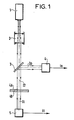
- the reference 1 designates a monochromatic light source such as a helium-neon laser.
- the width of the light beam is adjusted by means of an expander 2.
- a separator 3 for example a thin blade of semi-reflecting glass, separates the light beam into two parts.
- a first part of the light beam, of intensity Io is sent to a first linear opto-electronic converter 4 which can be a photodiode.
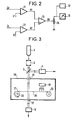
- FIG. 2 represents a block diagram of the electronic circuit forming part of the measuring device of the invention.
- Logarithmic amplifiers are attacked by current, which allows them to be linear over six decades to the nearest 0.1%, for example from 1 mA to 1nA.
- the outputs of the logarithmic amplifiers 11 and 12 are sent to a subtractor circuit 13 which outputs a signal
- An output potentiometer 15 makes it possible to supply a display member 16 directly graduated in unit of length.
- the taring is done in a known manner with a standard sample.
- a threshold circuit 17 When the device is used in an installation for engraving electronic circuits by plasma attack, a threshold circuit 17, receiving a set value, provides an end of attack signal, when the desired thickness is obtained.
- the invention advantageously applies to the control of the thickness of a layer deposited on a film.
- the material of the layer is titanium deposited on a film of polyethylene terephthalate.
- the layer must for example have a thickness of 400 angstroms.
- FIG. 3 shows, very schematically, the installation.
- the film 20 is stretched between a take-up reel 21 driven by a motor 22 and a supply reel 23.
- the assembly is placed in a sealed vacuum enclosure 25, comprising two portholes 26 and 27 facing each other.
- the incident light beam passes through the window 26, the film 20, the window 27 and is received by the converter 5.
- a device 30 for deposition under vacuum of known type sprays a layer of titanium on the film.
- the consistency of the thickness is ensured for example by a permanent adjustment of the speed of unwinding of the film, all the other parameters being kept constant.
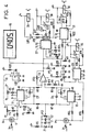
- FIG. 4 A detailed embodiment of the corresponding electronic circuit is given in FIG. 4.
- the references common to FIGS. 1 to 4 have been given the same reference number.
- Logarithmic amplifiers 11 and 12 are LOG 100 BURR - BROWN circuits.
- Circuit P1, R3 includes an IG switch with indications LEDs LD7 (green) and LD8 (red).
- the 7-segment diode display circuit is symbolized by the rectangle 16.
- Circuit 27 is a comparator with two thresholds, one lower (390 angstroms for example) controlling a relay 28 which closes a motor acceleration circuit, the other upper (410 angstroms) controlling a relay 29 which closes a circuit engine slowdown.
- the circuit 31 is a comparator circuit adjusted with a very high threshold, detecting the end of the unwinding of the strip which for this purpose carries, at its end, a portion made opaque.
- the circuit 31 controls a relay 32, the operation of which causes the installation to stop.
- the circuit 33 is a comparator set to a low threshold making it possible to control the operation of the laser and receiving the signal from the converter 5 as input. It controls a relay for protecting the installation in the event of a laser failure.
- the invention applies to all kinds of layer thickness control, in deposition as in etching, whenever the layer can be crossed by a light ray.
Landscapes
- Physics & Mathematics (AREA)
- General Physics & Mathematics (AREA)
- Length Measuring Devices By Optical Means (AREA)
Applications Claiming Priority (2)
| Application Number | Priority Date | Filing Date | Title |
|---|---|---|---|
| FR8214035A FR2531775A1 (fr) | 1982-08-12 | 1982-08-12 | Dispositif de mesure de l'epaisseur d'une couche deposee sur un substrat transparent |
| FR8214035 | 1982-08-12 |
Publications (1)
| Publication Number | Publication Date |
|---|---|
| EP0101997A1 true EP0101997A1 (fr) | 1984-03-07 |
Family
ID=9276825
Family Applications (1)
| Application Number | Title | Priority Date | Filing Date |
|---|---|---|---|
| EP83107844A Withdrawn EP0101997A1 (fr) | 1982-08-12 | 1983-08-09 | Dispositif de mesure de l'épaisseur d'une couche déposée sur un substrat transparent |
Country Status (3)
| Country | Link |
|---|---|
| EP (1) | EP0101997A1 (enExample) |
| JP (1) | JPS5948605A (enExample) |
| FR (1) | FR2531775A1 (enExample) |
Cited By (3)
| Publication number | Priority date | Publication date | Assignee | Title |
|---|---|---|---|---|
| WO1996033387A1 (de) * | 1995-04-21 | 1996-10-24 | Optikzentrum Nrw Gmbh (Oz) | Verfahren und vorrichtung zum messen der dicke dünner farbiger schichten |
| EP0749000A3 (en) * | 1995-06-16 | 1998-06-17 | International Business Machines Corporation | Method and apparatus for color thickness testing |
| CN107687815A (zh) * | 2017-07-31 | 2018-02-13 | 深港产学研基地 | 透光薄膜厚度测量方法、系统及终端设备 |
Families Citing this family (2)
| Publication number | Priority date | Publication date | Assignee | Title |
|---|---|---|---|---|
| RU2210558C2 (ru) * | 2001-01-19 | 2003-08-20 | Федеральное государственное унитарное предприятие "Муромский приборостроительный завод" | Устройство контроля сплошности напыления взрывчатого вещества на поверхность канала ударно-волновой трубки |
| JP2006300811A (ja) * | 2005-04-22 | 2006-11-02 | Hitachi Displays Ltd | 薄膜の膜厚測定方法、多結晶半導体薄膜の形成方法、半導体デバイスの製造方法、およびその製造装置、並びに画像表示装置の製造方法 |
Citations (2)
| Publication number | Priority date | Publication date | Assignee | Title |
|---|---|---|---|---|
| US3743429A (en) * | 1970-05-18 | 1973-07-03 | Kyoto Daiichi Kogaku Kk | Colorimeter for measuring concentration and indicating the concentration as a digital quantity |
| FR2356191A1 (fr) * | 1976-06-21 | 1978-01-20 | Leybold Heraeus Gmbh & Co Kg | Montage et photometre pour la mesure et la commande de l'epaisseur de couches minces optiques |
Family Cites Families (2)
| Publication number | Priority date | Publication date | Assignee | Title |
|---|---|---|---|---|
| JPS52153468A (en) * | 1976-06-15 | 1977-12-20 | Fujitsu Ltd | Thickness measuring method of substrates |
| JPS5674607A (en) * | 1979-11-26 | 1981-06-20 | Diafoil Co Ltd | Film thickness measuring device |
-
1982
- 1982-08-12 FR FR8214035A patent/FR2531775A1/fr active Granted
-
1983
- 1983-08-09 EP EP83107844A patent/EP0101997A1/fr not_active Withdrawn
- 1983-08-11 JP JP14726783A patent/JPS5948605A/ja active Pending
Patent Citations (2)
| Publication number | Priority date | Publication date | Assignee | Title |
|---|---|---|---|---|
| US3743429A (en) * | 1970-05-18 | 1973-07-03 | Kyoto Daiichi Kogaku Kk | Colorimeter for measuring concentration and indicating the concentration as a digital quantity |
| FR2356191A1 (fr) * | 1976-06-21 | 1978-01-20 | Leybold Heraeus Gmbh & Co Kg | Montage et photometre pour la mesure et la commande de l'epaisseur de couches minces optiques |
Cited By (3)
| Publication number | Priority date | Publication date | Assignee | Title |
|---|---|---|---|---|
| WO1996033387A1 (de) * | 1995-04-21 | 1996-10-24 | Optikzentrum Nrw Gmbh (Oz) | Verfahren und vorrichtung zum messen der dicke dünner farbiger schichten |
| EP0749000A3 (en) * | 1995-06-16 | 1998-06-17 | International Business Machines Corporation | Method and apparatus for color thickness testing |
| CN107687815A (zh) * | 2017-07-31 | 2018-02-13 | 深港产学研基地 | 透光薄膜厚度测量方法、系统及终端设备 |
Also Published As
| Publication number | Publication date |
|---|---|
| FR2531775B1 (enExample) | 1985-01-25 |
| FR2531775A1 (fr) | 1984-02-17 |
| JPS5948605A (ja) | 1984-03-19 |
Similar Documents
| Publication | Publication Date | Title |
|---|---|---|
| EP0291394B1 (fr) | Capteur de déplacement à fibres optiques décalées | |
| EP0243447A1 (en) | Nondispersive gas analyzer having no moving parts | |
| CA1279203C (fr) | Appareil de spectro-colorimetrie a fibres optiques | |
| EP0027763B1 (fr) | Procédé et appareil de mesure de distance par interférométrie laser à deux longueurs d'ondes | |
| FR2484639A1 (fr) | Dispositif de mesure de temperature a fibres optiques | |
| FR2532427A1 (fr) | Procede et dispositif pour la mesure de l'encrassement d'un detecteur capacitif de point de rosee | |
| EP0015820A1 (fr) | Dispositif pour la mesure des vitesses linéaires sans contact et sans marquage | |
| EP0029777A1 (fr) | Atténuateur optique à atténuation contrôlée | |
| FR2593604A1 (fr) | Procede et dispositif pour mesurer a distance la distribution d'un parametre physico-chimique dans un milieu | |
| FR2512545A1 (fr) | Procede et dispositif photometrique pour mesurer et regler l'epaisseur de couches a effet optique pendant leur formation sous vide | |
| EP0101997A1 (fr) | Dispositif de mesure de l'épaisseur d'une couche déposée sur un substrat transparent | |
| FR2356191A1 (fr) | Montage et photometre pour la mesure et la commande de l'epaisseur de couches minces optiques | |
| US3804532A (en) | Transparent film uniformity gauge | |
| FR2748562A1 (fr) | Procede et dispositif a deux cameras d'observation pour des mesures tridimensionnelles d'une structure complexe | |
| FR2591764A1 (fr) | Systeme optique de multiplexage et procede d'utilisation de ce systeme | |
| EP0670487B1 (fr) | Procédé et dispositif de détermination de l'absorption d'un rayonnement électromagnétique par un gaz | |
| EP0466598A1 (fr) | Procédé et installation de dépôt de couches antireflet et de contrôle de leur épaisseur | |
| EP0101049B1 (fr) | Dispositif de contrôle d'épaisseur de couches minces faiblement absorbantes | |
| FR2632403A1 (fr) | Pyrometre optique a au moins une fibre | |
| US4730109A (en) | Apparatus and method for measuring electric field by electroreflectance | |
| EP0246130A1 (fr) | Capteur de mesure linéaire sans contact de la distance d'une cible par rayonnement rétrodiffusé | |
| EP0515273B1 (fr) | Dispositif optique pour la reconnaissance de teintes de vitres | |
| EP0027758A1 (fr) | Dispositif de contrôle automatique de gain à action optique dans un système de transmission de signaux électriques par liaison optique | |
| FR2632723A1 (fr) | Systeme de detection pour photometre | |
| JPS61223541A (ja) | 表面検査方法および装置 |
Legal Events
| Date | Code | Title | Description |
|---|---|---|---|
| PUAI | Public reference made under article 153(3) epc to a published international application that has entered the european phase |
Free format text: ORIGINAL CODE: 0009012 |
|
| AK | Designated contracting states |
Designated state(s): AT BE CH DE FR GB IT LI LU NL SE |
|
| 17P | Request for examination filed |
Effective date: 19840906 |
|
| STAA | Information on the status of an ep patent application or granted ep patent |
Free format text: STATUS: THE APPLICATION IS DEEMED TO BE WITHDRAWN |
|
| 18D | Application deemed to be withdrawn |
Effective date: 19851127 |
|
| RIN1 | Information on inventor provided before grant (corrected) |
Inventor name: CANTELOUP, JEAN |