EP0101997A1 - Device for measuring the thickness of a film deposited on a transparent substrate - Google Patents
Device for measuring the thickness of a film deposited on a transparent substrate Download PDFInfo
- Publication number
- EP0101997A1 EP0101997A1 EP83107844A EP83107844A EP0101997A1 EP 0101997 A1 EP0101997 A1 EP 0101997A1 EP 83107844 A EP83107844 A EP 83107844A EP 83107844 A EP83107844 A EP 83107844A EP 0101997 A1 EP0101997 A1 EP 0101997A1
- Authority
- EP
- European Patent Office
- Prior art keywords
- output
- thickness
- logarithmic amplifier
- sent
- sample
- Prior art date
- Legal status (The legal status is an assumption and is not a legal conclusion. Google has not performed a legal analysis and makes no representation as to the accuracy of the status listed.)
- Withdrawn
Links
Images
Classifications
-
- G—PHYSICS
- G01—MEASURING; TESTING
- G01B—MEASURING LENGTH, THICKNESS OR SIMILAR LINEAR DIMENSIONS; MEASURING ANGLES; MEASURING AREAS; MEASURING IRREGULARITIES OF SURFACES OR CONTOURS
- G01B11/00—Measuring arrangements characterised by the use of optical techniques
- G01B11/02—Measuring arrangements characterised by the use of optical techniques for measuring length, width or thickness
- G01B11/06—Measuring arrangements characterised by the use of optical techniques for measuring length, width or thickness for measuring thickness ; e.g. of sheet material
- G01B11/0616—Measuring arrangements characterised by the use of optical techniques for measuring length, width or thickness for measuring thickness ; e.g. of sheet material of coating
Abstract
Description
La présente invention concerne un dispositif opto-électronique de mesure de l'épaisseur d'une couche mince d'un matériau déposé sur un substrat transparent.The present invention relates to an opto-electronic device for measuring the thickness of a thin layer of a material deposited on a transparent substrate.
Le dispositif est fondé sur l'absorption, par le matériau d'un rayonnement lumineux et s'applique aux matériaux pour lesquels il existe une loi d'absorption lumineuse du typeThe device is based on the absorption by the material of light radiation and applies to materials for which there is a light absorption law of the type
It = Ito exp ( - a e) (Loi de Beer-Lambert) où :
- Ito = est l'intensité lumineuse envoyée normalement sur l'échantillon
- It = est l'intensité lumineuse transmise
- e = l'épaisseur de l'échantillon
- a = le coefficient d'absoption de l'échantillon.
- Ito = is the light intensity normally sent to the sample
- It = is the transmitted light intensity
- e = the thickness of the sample
- a = the absorption coefficient of the sample.
L'épaisseur e est alors égale à 1/a Log (Ito / It).The thickness e is then equal to 1 / a Log (Ito / It).
Un but de l'invention est de réaliser un dispositif optique de mesure de l'épaisseur d'un échantillon qui fournisse directement une valeur de l'épaisseur.An object of the invention is to provide an optical device for measuring the thickness of a sample which directly provides a value for the thickness.
Un autre but de l'invention est de réaliser un dispositif optique de mesure dont le résultat soit insensible aux fluctuations éventuelles de l'intensité de la source lumineuse utilisée.Another object of the invention is to provide an optical measurement device the result of which is insensitive to possible fluctuations in the intensity of the light source used.
L'invention a pour objet un dispositif pour la mesure de l'épaisseur d'une couche déposée sur un substrat transparent, le matériau de la ' couche ayant une loi d'absorption lumineuse du type exponentiel, caractérisé en ce qu'il comprend
- - une source de lumière monochromatique,
- - un séparateur de lumière partageant le faisceau émis par la source en deux parties, une première partie envoyée sur un premier convertisseur opto-électronique fournissant en sortie un premier signal électrique envoyé sur un premier amplificateur logarithmique, une seconde partie envoyée normalement à l'échantillon, le faisceau transmis étant reçu sur un second convertisseur opto-électronique fournissant en sortie un second signal électrique envoyé sur un second amplificateur logarithmique, les sorties des deux amplificateurs étant reliées à l'entrée d'un circuit soustracteur fournissant en sortie un signal proportionnel à la différence entre le signal de sortie du second amplificateur logarithmique et le signal de sortie du premier amplificateur logarithmique, cette différence étant représentative de l'épaisseur de l'échantillon.
- - a monochromatic light source,
- - a light splitter dividing the beam emitted by the source into two parts, a first part sent to a first opto-electronic converter providing as output a first electrical signal sent to a first logarithmic amplifier, a second part normally sent to the sample , the transmitted beam being received on a second opto-electronic converter providing at output a second electrical signal sent on a second logarithmic amplifier, the outputs of the two amplifiers being connected to the input of a subtractor circuit providing at output a signal proportional to the difference between the output signal of the second logarithmic amplifier and the output signal of the first logarithmic amplifier, this difference being representative of the thickness of the sample.
L'invention sera bien comprise par la description donnée ci-après d'un mode préféré de réalisation de l'invention en référence au dessin annexé dans lequel :
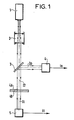
- - la figure 1 est un schéma de la partie optique du dispositif de mesure de l'invention,
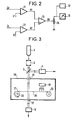
- - la figure 2 est un schéma de la partie électronique du dispositif de mesure de l'invention,
- - la figure 3 est un schéma d'une installation faisant application du dispositif de l'invention pour le contrôle de l'épaisseur d'une couche déposée sur un film,
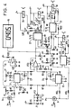
- - la figure 4 est un schéma détaillé d'un mode préféré de réalisation de la partie électronique de l'installation de la figure 3.
- FIG. 1 is a diagram of the optical part of the measuring device of the invention,
- FIG. 2 is a diagram of the electronic part of the measuring device of the invention,
- FIG. 3 is a diagram of an installation applying the device of the invention for controlling the thickness of a layer deposited on a film,
- FIG. 4 is a detailed diagram of a preferred embodiment of the electronic part of the installation of FIG. 3.
Dans la figure 1, la référence 1 désigne une source de lumière monochromatique telle qu'un laser hélium-néon. La largeur du faisceau lumineux est ajustée au moyen d'un expanseur 2. Un séparateur 3, par exemple une mince lame de verre semi-réfléchissante, sépare le faisceau lumineux en deux parties. Une première partie du faisceau lumineux, d'intensité Io, est envoyée sur un premier convertisseur opto-électronique linéaire 4 qui peut être une photodiode.In FIG. 1, the reference 1 designates a monochromatic light source such as a helium-neon laser. The width of the light beam is adjusted by means of an
Ce convertisseur fournit en sortie un signal électrique io = S2 Io, ou S2 est un coefficient de proportionnalité.This converter supplies an electrical signal io = S2 Io, where S2 is a proportionality coefficient.
Une seconde partie du faisceau lumineux d'intensité I2 traverse l'échantillon comprenant, sur un substrat transparent 4B, une couche 4A dont on veut mesurer l'épaisseur ; le faisceau lumineux issu de l'échantillon, d'intensité It, est envoyé sur un second convertisseur opto-électronique linéaire 5 du même type que le convertisseur 4. Il fournit en sortie un signal électrique it = S1 It, où S1 est un coefficient de proportionnalité.A second part of the light beam of intensity I2 passes through the sample comprising, on a
La figure 2 représente un schéma par blocs du circuit électronique faisant partie du dispositif de mesure de l'invention.FIG. 2 represents a block diagram of the electronic circuit forming part of the measuring device of the invention.
Les signaux io et it sont reçus sur des amplificateurs opérationnels (respectivement 11 et 12) effectuant le logarithme des signaux d'entrée, à une constante additive près. Les signaux de sortie V1 et V2 des amplificateurs 11 et 12 sont liés par les relations :
- V1 = K1 Log (S1 It/ir) + A1
- V2 = K2 Log (S2 Io/ir) + A2
où K1, K2 sont des coefficients de proportionnalité égaux à une même valeur K si les amplificateurs 11 et 12 sont identiques,
ir est le courant commun de référence appliqué aux amplificateurs 11 et 12,
A1 et A2 sont les valeurs d'off set des deux amplificateurs 11 et 12.The signals io and it are received on operational amplifiers (respectively 11 and 12) carrying out the logarithm of the input signals, to the nearest additive constant. The output signals V1 and V2 of
- V1 = K1 Log (S1 It / ir) + A1
- V2 = K2 Log (S2 Io / ir) + A2
where K1, K2 are coefficients of proportionality equal to the same value K if the
ir is the common reference current applied to
A1 and A2 are the off set values of the two
Les amplificateurs logarithmiques sont attaqués en courant, ce qui leur permet d'être linéaire sur six décades à 0,1% près, par exemple de 1 mA à 1nA.Logarithmic amplifiers are attacked by current, which allows them to be linear over six decades to the nearest 0.1%, for example from 1 mA to 1nA.
Les sorties des amplificateurs logarithmiques 11 et 12 sont envoyés à un circuit soustracteur 13 qui fournit en sortie un signal
Un potentiomètre de sortie 15 permet d'alimenter un organe d'affichage 16 directement gradué en unité de longueur. Le tarage est fait de manière connue avec un échantillon étalon.An
Lorsque le dispositif est utilisé dans une installation de gravure de circuits électroniques par attaque de plasma, un circuit à seuil 17, recevant une valeur de consigne, fournit un signal de fin d'attaque, lorsque l'épaisseur recherchée est obtenue.When the device is used in an installation for engraving electronic circuits by plasma attack, a threshold circuit 17, receiving a set value, provides an end of attack signal, when the desired thickness is obtained.
Le dispositif de l'invention présente divers avantages :
- - le résultat de la mesure est indépendant des fluctuations de la source lumineuse,
- - le choix d'amplificateurs logarithmiques permet d'obtenir une linéarité de la réponse au signaux d'entrées sur une vaste échelle s'étendant sur 6 décades,
- - le temps de réponse est très faible, de l'ordre de la milliseconde,
- - l'emploi d'un laser associé à un expanseur permet de focaliser le
- - the result of the measurement is independent of fluctuations in the light source,
- - the choice of logarithmic amplifiers makes it possible to obtain a linearity of the response to the input signals on a large scale extending over 6 decades,
- - the response time is very low, of the order of a millisecond,
- - the use of a laser associated with an expander makes it possible to focus the
faisceau à la surface de l'échantillon avec une grande souplesse associée à une grande précision.beam at the surface of the sample with great flexibility combined with high precision.
L'invention s'applique avantageusement au contrôle de l'épaisseur d'une couche déposée sur un film.The invention advantageously applies to the control of the thickness of a layer deposited on a film.
A titre d'exemple, le matériau de la couche est du titane déposé sur un film de polytéréphtalate d'éthylène-glycol.As an example, the material of the layer is titanium deposited on a film of polyethylene terephthalate.
La couche doit avoir par exemple une épaisseur de 400 angströms.The layer must for example have a thickness of 400 angstroms.
La figure 3 montre, très schématiquement, l'installation.Figure 3 shows, very schematically, the installation.
On reconnaît le laser 1, l'expanseur de faisceau 2, le séparateur 3, le premier convertisseur opto-électronique 4.We recognize the laser 1, the
Le film 20 est tendue entre une bobine réceptrice 21 entraînée par un moteur 22 et une bobine débitrice 23.The film 20 is stretched between a take-
L'ensemble est placée dans une enceinte étanche sous vide 25, comprenant deux hublots 26 et 27 se faisant face. Le faisceau lumineux incident traverse le hublot 26, le film 20, le hublot 27 et est reçu par le convertisseur 5.The assembly is placed in a sealed
Un dispositif 30 de dépôt sous vide de type connu pulvérise une couche de titane sur le film.A device 30 for deposition under vacuum of known type sprays a layer of titanium on the film.
La constance de l'épaisseur est assurée par exemple par un réglage permanent de la vitesse de déroulement du film, tous les autres paramètres étant maintenus constants.The consistency of the thickness is ensured for example by a permanent adjustment of the speed of unwinding of the film, all the other parameters being kept constant.
Un mode détaillé de réalisation du circuit électonique correspondant est donné dans la figure 4. Les références communes aux figures 1 à 4 ont reçu le même numéro de référence.A detailed embodiment of the corresponding electronic circuit is given in FIG. 4. The references common to FIGS. 1 to 4 have been given the same reference number.
On distingue dans la figure 4 les deux convertisseurs 4 et 5 recevant les flux lumineux Io et It. Les amplificateurs logarithmiques 11 et 12 sont des circuits LOG 100 BURR - BROWN. La référence courant est donné par le circuit Z1, C1, C2, P12, R6, R7, avec les significations suivantes des lettres : C = condensateur, R = résistance, Z = diode . Zener, P potentiomètre.We distinguish in Figure 4 the two
Ces symboles se retrouvent dans la suite avec également :
- LD = Led (diode électroluminescente)
- RL = relais
- V+, v- tensions continues de commande des circuits.
- LD = Led (light emitting diode)
- RL = relay
- V + , v - continuous control voltages for circuits.
Le circuit P1, R3 comprend un interrupteur IG avec indications visuelles par les diodes LD7 (verte) et LD8 (rouge).Circuit P1, R3 includes an IG switch with indications LEDs LD7 (green) and LD8 (red).
Le circuit d'affichage à diodes 7 segments est symbolisé par le rectangle 16.The 7-segment diode display circuit is symbolized by the
Le circuit 27 est un comparateur à deux seuils, l'un inférieur (390 angstroms par exemple) commandant un relais 28 qui ferme un circuit d'accélération du moteur, l'autre supérieur (410 angströms) commandant un relais 29 qui ferme un circuit de ralentissement du moteur.
Le circuit 31 est un circuit comparateur réglé avec un seuil très élevé, détectant la fin du déroulement de la bande qui porte à cet effet, à son extrémité, une portion rendue opaque.The
Le circuit 31 commande un relais 32 dont le fonctionnement provoque un arrêt de l'installation.The
Le circuit 33 est un comparateur réglé à un seuil bas permettant de contrôler le fonctionnement du laser et recevant en entrée le signal du convertisseur 5. Il commande un relais de protection de l'installation en cas de défaillance du laser.The
L'application qui vient d'être décrite n'est qu'un exemple.The application which has just been described is only an example.
L'invention s'applique pour toutes sortes de contrôle d'épaisseurs de couches, en dépôt comme en gravure, toutes les fois que la couche peut être traversée par un rayon lumineux.The invention applies to all kinds of layer thickness control, in deposition as in etching, whenever the layer can be crossed by a light ray.
Claims (1)
Applications Claiming Priority (2)
| Application Number | Priority Date | Filing Date | Title |
|---|---|---|---|
| FR8214035 | 1982-08-12 | ||
| FR8214035A FR2531775A1 (en) | 1982-08-12 | 1982-08-12 | DEVICE FOR MEASURING THE THICKNESS OF A LAYER DEPOSITED ON A TRANSPARENT SUBSTRATE |
Publications (1)
| Publication Number | Publication Date |
|---|---|
| EP0101997A1 true EP0101997A1 (en) | 1984-03-07 |
Family
ID=9276825
Family Applications (1)
| Application Number | Title | Priority Date | Filing Date |
|---|---|---|---|
| EP83107844A Withdrawn EP0101997A1 (en) | 1982-08-12 | 1983-08-09 | Device for measuring the thickness of a film deposited on a transparent substrate |
Country Status (3)
| Country | Link |
|---|---|
| EP (1) | EP0101997A1 (en) |
| JP (1) | JPS5948605A (en) |
| FR (1) | FR2531775A1 (en) |
Cited By (3)
| Publication number | Priority date | Publication date | Assignee | Title |
|---|---|---|---|---|
| WO1996033387A1 (en) * | 1995-04-21 | 1996-10-24 | Optikzentrum Nrw Gmbh (Oz) | Process and device for measuring the thickness of thin coloured films |
| EP0749000A2 (en) * | 1995-06-16 | 1996-12-18 | International Business Machines Corporation | Method and apparatus for color thickness testing |
| CN107687815A (en) * | 2017-07-31 | 2018-02-13 | 深港产学研基地 | Light transmission film method for measuring thickness, system and terminal device |
Families Citing this family (1)
| Publication number | Priority date | Publication date | Assignee | Title |
|---|---|---|---|---|
| JP2006300811A (en) * | 2005-04-22 | 2006-11-02 | Hitachi Displays Ltd | Method of measuring film thickness of thin film, method of forming polycrystal semiconductor thin film, manufacturing method for semiconductor device, manufacturing apparatus for the same, and manufacture method for image display |
Citations (2)
| Publication number | Priority date | Publication date | Assignee | Title |
|---|---|---|---|---|
| US3743429A (en) * | 1970-05-18 | 1973-07-03 | Kyoto Daiichi Kogaku Kk | Colorimeter for measuring concentration and indicating the concentration as a digital quantity |
| FR2356191A1 (en) * | 1976-06-21 | 1978-01-20 | Leybold Heraeus Gmbh & Co Kg | MOUNTING AND PHOTOMETER FOR MEASUREMENT AND CONTROL OF THE THICKNESS OF OPTICAL THIN LAYERS |
Family Cites Families (2)
| Publication number | Priority date | Publication date | Assignee | Title |
|---|---|---|---|---|
| JPS52153468A (en) * | 1976-06-15 | 1977-12-20 | Fujitsu Ltd | Thickness measuring method of substrates |
| JPS5674607A (en) * | 1979-11-26 | 1981-06-20 | Diafoil Co Ltd | Film thickness measuring device |
-
1982
- 1982-08-12 FR FR8214035A patent/FR2531775A1/en active Granted
-
1983
- 1983-08-09 EP EP83107844A patent/EP0101997A1/en not_active Withdrawn
- 1983-08-11 JP JP14726783A patent/JPS5948605A/en active Pending
Patent Citations (2)
| Publication number | Priority date | Publication date | Assignee | Title |
|---|---|---|---|---|
| US3743429A (en) * | 1970-05-18 | 1973-07-03 | Kyoto Daiichi Kogaku Kk | Colorimeter for measuring concentration and indicating the concentration as a digital quantity |
| FR2356191A1 (en) * | 1976-06-21 | 1978-01-20 | Leybold Heraeus Gmbh & Co Kg | MOUNTING AND PHOTOMETER FOR MEASUREMENT AND CONTROL OF THE THICKNESS OF OPTICAL THIN LAYERS |
Cited By (4)
| Publication number | Priority date | Publication date | Assignee | Title |
|---|---|---|---|---|
| WO1996033387A1 (en) * | 1995-04-21 | 1996-10-24 | Optikzentrum Nrw Gmbh (Oz) | Process and device for measuring the thickness of thin coloured films |
| EP0749000A2 (en) * | 1995-06-16 | 1996-12-18 | International Business Machines Corporation | Method and apparatus for color thickness testing |
| EP0749000A3 (en) * | 1995-06-16 | 1998-06-17 | International Business Machines Corporation | Method and apparatus for color thickness testing |
| CN107687815A (en) * | 2017-07-31 | 2018-02-13 | 深港产学研基地 | Light transmission film method for measuring thickness, system and terminal device |
Also Published As
| Publication number | Publication date |
|---|---|
| FR2531775A1 (en) | 1984-02-17 |
| JPS5948605A (en) | 1984-03-19 |
| FR2531775B1 (en) | 1985-01-25 |
Similar Documents
| Publication | Publication Date | Title |
|---|---|---|
| EP0291394B1 (en) | Displacement sensor with recessed optical fibres | |
| CA1279203C (en) | Optical fiber spectro-colorimetry apparatus | |
| CA1129553A (en) | Apparatus for measuring the sebum secreted by the skin | |
| EP0243447A1 (en) | Nondispersive gas analyzer having no moving parts | |
| FR2484639A1 (en) | OPTICAL FIBER TEMPERATURE MEASURING DEVICE | |
| EP0027763B1 (en) | Process and apparatus for measuring distance by laser interferometry with two wavelengths | |
| EP0029777A1 (en) | Optical attenuator with controlled attenuation | |
| FR2512545A1 (en) | METHOD AND PHOTOMETRIC DEVICE FOR MEASURING AND ADJUSTING THE THICKNESS OF OPTICAL LAYERS DURING THE VACUUM FORMATION THEREOF | |
| FR2593604A1 (en) | METHOD AND DEVICE FOR REMOTELY MEASURING THE DISTRIBUTION OF A PHYSICO-CHEMICAL PARAMETER IN A MEDIUM | |
| FR2356191A1 (en) | MOUNTING AND PHOTOMETER FOR MEASUREMENT AND CONTROL OF THE THICKNESS OF OPTICAL THIN LAYERS | |
| EP0101997A1 (en) | Device for measuring the thickness of a film deposited on a transparent substrate | |
| FR2748562A1 (en) | METHOD AND DEVICE WITH TWO OBSERVATION CAMERAS FOR THREE-DIMENSIONAL MEASUREMENTS OF A COMPLEX STRUCTURE | |
| FR2591764A1 (en) | OPTICAL MULTIPLEXING SYSTEM AND METHOD OF USING THE SAME | |
| EP0670487B1 (en) | Method and device for the determining of the absorption of an electromagnetic radiation by a gas | |
| EP0466598A1 (en) | Method and apparatus for deposition of antireflection coatings and control of their thickness | |
| FR2632403A1 (en) | OPTICAL PYROMETER HAS AT LEAST ONE FIBER | |
| EP0101049B1 (en) | Device for monitoring the thickness of thin, hardly absorbing films | |
| US4730109A (en) | Apparatus and method for measuring electric field by electroreflectance | |
| FR2632723A1 (en) | Detection system for photometer | |
| EP0246130A1 (en) | Detector for the linear, non-contacting measurement of the distance to a target using scattered radiation | |
| FR2676811A1 (en) | OPTICAL DEVICE FOR RECOGNIZING GLASS SHADES. | |
| EP0027758A1 (en) | Automatic gain control device using optical means in a system for transmitting electric signals by an optical link | |
| FR2557997A1 (en) | Interactive display device comprising a scanning screen | |
| FR2518745A1 (en) | DEVICE FOR MEASURING THE TEMPERATURE OF AN OBJECT FROM THE INFRARED RADIATION ISSUED THEREIN | |
| Kim et al. | Post-Calibration Correction for a Rotating-Analyzer Ellipsometer with an Optical Fiber Bundle Detection System |
Legal Events
| Date | Code | Title | Description |
|---|---|---|---|
| PUAI | Public reference made under article 153(3) epc to a published international application that has entered the european phase |
Free format text: ORIGINAL CODE: 0009012 |
|
| AK | Designated contracting states |
Designated state(s): AT BE CH DE FR GB IT LI LU NL SE |
|
| 17P | Request for examination filed |
Effective date: 19840906 |
|
| STAA | Information on the status of an ep patent application or granted ep patent |
Free format text: STATUS: THE APPLICATION IS DEEMED TO BE WITHDRAWN |
|
| 18D | Application deemed to be withdrawn |
Effective date: 19851127 |
|
| RIN1 | Information on inventor provided before grant (corrected) |
Inventor name: CANTELOUP, JEAN |