EP0101374B1 - Embase pour laser à semi-conducteur et son procédé de fabrication - Google Patents
Embase pour laser à semi-conducteur et son procédé de fabrication Download PDFInfo
- Publication number
- EP0101374B1 EP0101374B1 EP83401626A EP83401626A EP0101374B1 EP 0101374 B1 EP0101374 B1 EP 0101374B1 EP 83401626 A EP83401626 A EP 83401626A EP 83401626 A EP83401626 A EP 83401626A EP 0101374 B1 EP0101374 B1 EP 0101374B1
- Authority
- EP
- European Patent Office
- Prior art keywords
- slot
- strip
- support
- base
- pedestal
- Prior art date
- Legal status (The legal status is an assumption and is not a legal conclusion. Google has not performed a legal analysis and makes no representation as to the accuracy of the status listed.)
- Expired
Links
- 239000000758 substrate Substances 0.000 title claims description 10
- 239000004065 semiconductor Substances 0.000 title claims description 9
- 238000000034 method Methods 0.000 title claims description 7
- 238000004519 manufacturing process Methods 0.000 title description 8
- 229910052751 metal Inorganic materials 0.000 claims description 16
- 239000002184 metal Substances 0.000 claims description 16
- 229910045601 alloy Inorganic materials 0.000 claims description 10
- 239000000956 alloy Substances 0.000 claims description 10
- 238000002844 melting Methods 0.000 claims description 7
- 230000008018 melting Effects 0.000 claims description 7
- 238000005498 polishing Methods 0.000 claims description 7
- 239000010949 copper Substances 0.000 claims description 5
- PCHJSUWPFVWCPO-UHFFFAOYSA-N gold Chemical compound [Au] PCHJSUWPFVWCPO-UHFFFAOYSA-N 0.000 claims description 5
- 229910052737 gold Inorganic materials 0.000 claims description 5
- 239000010931 gold Substances 0.000 claims description 5
- 238000003801 milling Methods 0.000 claims description 5
- 238000005096 rolling process Methods 0.000 claims description 5
- RYGMFSIKBFXOCR-UHFFFAOYSA-N Copper Chemical compound [Cu] RYGMFSIKBFXOCR-UHFFFAOYSA-N 0.000 claims description 4
- PXHVJJICTQNCMI-UHFFFAOYSA-N Nickel Chemical compound [Ni] PXHVJJICTQNCMI-UHFFFAOYSA-N 0.000 claims description 4
- PNEYBMLMFCGWSK-UHFFFAOYSA-N aluminium oxide Inorganic materials [O-2].[O-2].[O-2].[Al+3].[Al+3] PNEYBMLMFCGWSK-UHFFFAOYSA-N 0.000 claims description 4
- 229910052802 copper Inorganic materials 0.000 claims description 4
- 238000005520 cutting process Methods 0.000 claims description 3
- 238000003754 machining Methods 0.000 claims description 3
- 238000007650 screen-printing Methods 0.000 claims description 3
- 238000005476 soldering Methods 0.000 claims description 3
- 229910052759 nickel Inorganic materials 0.000 claims description 2
- 229910052709 silver Inorganic materials 0.000 claims description 2
- 239000004332 silver Substances 0.000 claims description 2
- NJPPVKZQTLUDBO-UHFFFAOYSA-N novaluron Chemical compound C1=C(Cl)C(OC(F)(F)C(OC(F)(F)F)F)=CC=C1NC(=O)NC(=O)C1=C(F)C=CC=C1F NJPPVKZQTLUDBO-UHFFFAOYSA-N 0.000 claims 7
- KDLHZDBZIXYQEI-UHFFFAOYSA-N Palladium Chemical compound [Pd] KDLHZDBZIXYQEI-UHFFFAOYSA-N 0.000 claims 2
- 238000000227 grinding Methods 0.000 claims 2
- 238000005552 hardfacing Methods 0.000 claims 1
- 238000009413 insulation Methods 0.000 claims 1
- 229910052763 palladium Inorganic materials 0.000 claims 1
- 239000000945 filler Substances 0.000 description 4
- 239000002904 solvent Substances 0.000 description 4
- VEXZGXHMUGYJMC-UHFFFAOYSA-N Hydrochloric acid Chemical compound Cl VEXZGXHMUGYJMC-UHFFFAOYSA-N 0.000 description 2
- 241000446313 Lamella Species 0.000 description 2
- 229910001128 Sn alloy Inorganic materials 0.000 description 2
- 238000005219 brazing Methods 0.000 description 2
- 239000011248 coating agent Substances 0.000 description 2
- 238000000576 coating method Methods 0.000 description 2
- 238000005238 degreasing Methods 0.000 description 2
- SWELZOZIOHGSPA-UHFFFAOYSA-N palladium silver Chemical compound [Pd].[Ag] SWELZOZIOHGSPA-UHFFFAOYSA-N 0.000 description 2
- 229910052787 antimony Inorganic materials 0.000 description 1
- WATWJIUSRGPENY-UHFFFAOYSA-N antimony atom Chemical compound [Sb] WATWJIUSRGPENY-UHFFFAOYSA-N 0.000 description 1
- 238000005452 bending Methods 0.000 description 1
- 230000004927 fusion Effects 0.000 description 1
- 239000011521 glass Substances 0.000 description 1
- 238000009434 installation Methods 0.000 description 1
- 239000000463 material Substances 0.000 description 1
- 239000000155 melt Substances 0.000 description 1
- 230000005855 radiation Effects 0.000 description 1
- 230000035945 sensitivity Effects 0.000 description 1
- 239000010935 stainless steel Substances 0.000 description 1
- 229910001220 stainless steel Inorganic materials 0.000 description 1
- 238000004381 surface treatment Methods 0.000 description 1
- 235000012431 wafers Nutrition 0.000 description 1
Images
Classifications
-
- H—ELECTRICITY
- H01—ELECTRIC ELEMENTS
- H01S—DEVICES USING THE PROCESS OF LIGHT AMPLIFICATION BY STIMULATED EMISSION OF RADIATION [LASER] TO AMPLIFY OR GENERATE LIGHT; DEVICES USING STIMULATED EMISSION OF ELECTROMAGNETIC RADIATION IN WAVE RANGES OTHER THAN OPTICAL
- H01S5/00—Semiconductor lasers
- H01S5/02—Structural details or components not essential to laser action
- H01S5/022—Mountings; Housings
- H01S5/023—Mount members, e.g. sub-mount members
- H01S5/02315—Support members, e.g. bases or carriers
-
- H—ELECTRICITY
- H01—ELECTRIC ELEMENTS
- H01S—DEVICES USING THE PROCESS OF LIGHT AMPLIFICATION BY STIMULATED EMISSION OF RADIATION [LASER] TO AMPLIFY OR GENERATE LIGHT; DEVICES USING STIMULATED EMISSION OF ELECTROMAGNETIC RADIATION IN WAVE RANGES OTHER THAN OPTICAL
- H01S5/00—Semiconductor lasers
- H01S5/02—Structural details or components not essential to laser action
- H01S5/022—Mountings; Housings
- H01S5/0233—Mounting configuration of laser chips
-
- H—ELECTRICITY
- H01—ELECTRIC ELEMENTS
- H01S—DEVICES USING THE PROCESS OF LIGHT AMPLIFICATION BY STIMULATED EMISSION OF RADIATION [LASER] TO AMPLIFY OR GENERATE LIGHT; DEVICES USING STIMULATED EMISSION OF ELECTROMAGNETIC RADIATION IN WAVE RANGES OTHER THAN OPTICAL
- H01S5/00—Semiconductor lasers
- H01S5/02—Structural details or components not essential to laser action
- H01S5/022—Mountings; Housings
- H01S5/0235—Method for mounting laser chips
-
- H—ELECTRICITY
- H01—ELECTRIC ELEMENTS
- H01S—DEVICES USING THE PROCESS OF LIGHT AMPLIFICATION BY STIMULATED EMISSION OF RADIATION [LASER] TO AMPLIFY OR GENERATE LIGHT; DEVICES USING STIMULATED EMISSION OF ELECTROMAGNETIC RADIATION IN WAVE RANGES OTHER THAN OPTICAL
- H01S5/00—Semiconductor lasers
- H01S5/02—Structural details or components not essential to laser action
- H01S5/024—Arrangements for thermal management
- H01S5/02469—Passive cooling, e.g. where heat is removed by the housing as a whole or by a heat pipe without any active cooling element like a TEC
Definitions
- the subject of the present invention is a base for a semiconductor laser and its manufacturing process.
- a base for semiconductor laser is a part intended to serve as mechanical support for the semiconductor structure seat of the laser effect, to allow dissipation of the heat released in this structure and to facilitate electrical connections with a power source.
- a base for a semiconductor laser comprising a monobloc metal support having a prismatic part formed by two planes also inclined with respect to a plane of symmetry.
- the prismatic part having a polished upper field intended to receive a laser chip whose length is equal to the thickness of the polished upper field.
- a base for a semiconductor laser comprising a monobloc metal support, on which is brazed an interconnection plate of parallelepiped shape, constituted by an insulating substrate covered with a metal layer likely to be connected by a connection to the laser chip.
- the object of the present invention is precisely to remedy these drawbacks by proposing a base for which the part receiving the laser chip is narrow and does not exhibit bending and, which, moreover, leaves the laser mirrors accessible.
- a base comprising a one-piece metal support having a prismatic part formed by two planes also inclined relative to a plane of symmetry, this prismatic part being pierced with a slot made in this plane of symmetry, a metal strip being brazed in the slot, this strip having a polished upper field intended to receive a laser chip whose length is equal to the thickness of the strip, the support further having a flat base on which a interconnection plate of parallelepiped shape, this plate being constituted by an insulating substrate covered with a metallic layer capable of being connected by a connection to the laser chip.
- the support and the strip are made of copper.
- the interconnection plate is constituted by a sintered alumina substrate covered on one side by a conductive layer screen printed with gold, and on the other side (intended to be in contact with the base) by a heat conducting layer produced using a silver-palladium paste.
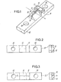
- the base shown in Figure 1 comprises a single piece metal support 10 having a prismatic portion 12 formed by two planes also inclined relative to the plane of symmetry of the assembly. This prismatic part is pierced with a slot 13 formed in the plane of symmetry. A metal strip 14 is brazed in the slot, this strip having a polished upper field intended to receive a laser chip 15. The length of this chip is equal to the thickness of the strip. The laser radiation is therefore directed transversely.
- the base further comprises a base 11 on which is brazed an interconnection plate 16 of parallelepiped shape.
- the support may include fixing holes 18.
- the prismatic shape 12 releases the laser chip and the mirrors without harming the thermal contact which remains established over the entire base of the laser chip.
- the manufacturing process for such a base can include the following operations, in which is only an example of implementation.
- the support is obtained by milling and rectifying a round or drawn copper, for example of the annealed Cu type.
- the part shown in FIG. 2 is obtained, with its base 11 and its prismatic part 12.
- the slot 13 is obtained by sawing on a milling machine using a width milling cutter such that the desired width is obtained in a single pass. This is equal to the thickness of the strip to be mounted, increased from 30 to 40 ⁇ .Lm.
- Deburring is then carried out, followed by degreasing with chlorinated or fluorinated solvents in an ultrasonic tank.
- the strip is then preferably made of annealed copper, as for the support.
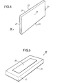
- the material is supplied with sheets from which strips 2.5 mm wide and about 250 mm long are drawn. Each strip is passed through a rolling mill to bring its thickness to that of the strip to ⁇ 1 ⁇ m. The strips coming out of the rolling are cut to a length of 4.5 mm using a saw mill. After cutting, the strips are cleaned using a chlorinated or fluorinated solvent. Each strip then undergoes rectification on three faces, referenced 23, 25, 26 in FIG. 4, the faces 21 and 22 remaining rough from rolling. The strips are then subject to polishing on their face 24 intended to receive the laser chip.
- the interconnection plate is shown in FIG. 5. It consists of a sintered alumina substrate 30 covered with a conductive layer 32 used for interconnection and produced by screen printing of a gold paste without glass. The underside used for fixing to the base of the support is covered with a layer 34 obtained using a silver-palladium paste. Several wafers can be screen-printed simultaneously and baked on an alumina substrate, which is then cut using laser beam machining equipment.
- the strip is fixed by soft soldering in the slot made in the support.
- the filler alloy is chosen according to its melting temperature and the thermal resistance characteristics requested from the base. For example, for resistance to 160 ° C., a 62.5% tin alloy, 36% lead, 1.5% silver can be used, the melting temperature of which is 179 ° C. For a resistance at 200 ° C., it is possible to use a 95% tin alloy 5% antimony whose melting temperature is 240 ° C.
- the lamella mounting operation comprises two phases: coating the faces of the slot with the filler metal, then brazing the lamella.
- the coating of the faces of the slot is carried out using a preform of the chosen filler alloy, which makes it possible to treat only the slot.
- the preform is engaged by centering it in the slot so that it is flush with the upper part.
- the support is brought to a temperature slightly higher than the melting temperature of the preform, for example by placing it on a hot plate.
- the preform melts by flowing over the sides and the bottom of the slot.
- a strip of stainless steel is passed through the slot, the thickness of which is equal to that of the slot minus 100 ⁇ m.
- a longitudinal back and forth movement is applied to the strip, which makes it possible to obtain a deposit without excess thickness.
- the flat part of the support to receive the interconnection plate is coated with the same alloy. The whole is cooled by placing the support on a good heat sink.
- the strip is engaged in the slot by centering it.
- the interconnection plate is placed in position on its support.
- the mounting support is brought to the melting temperature of the preform and pressure is applied to the ends of the strip allowing the latter to be brought into abutment at the bottom of the slot.
- the strip and the interconnection plate are brazed simultaneously.
- the part is cooled, then it is cleaned in a chlorinated solvent.
- the bases are then stored in a dehydrated enclosure.
- the assembled assembly can be subjected to a surface treatment by electrolytic deposits comprising a deposit of shiny nickel 0.5 to 1 ⁇ m thick, itself coated with a gold deposit of 0.4 at 0.6 ⁇ .Lm thick.
Landscapes
- Physics & Mathematics (AREA)
- Condensed Matter Physics & Semiconductors (AREA)
- General Physics & Mathematics (AREA)
- Electromagnetism (AREA)
- Optics & Photonics (AREA)
- Cooling Or The Like Of Semiconductors Or Solid State Devices (AREA)
- Semiconductor Lasers (AREA)
- Ceramic Products (AREA)
- Die Bonding (AREA)
Applications Claiming Priority (2)
| Application Number | Priority Date | Filing Date | Title |
|---|---|---|---|
| FR8214042A FR2531819A1 (fr) | 1982-08-12 | 1982-08-12 | Embase pour laser a semi-conducteur et son procede de fabrication |
| FR8214042 | 1982-08-12 |
Publications (3)
| Publication Number | Publication Date |
|---|---|
| EP0101374A2 EP0101374A2 (fr) | 1984-02-22 |
| EP0101374A3 EP0101374A3 (en) | 1984-04-11 |
| EP0101374B1 true EP0101374B1 (fr) | 1987-01-07 |
Family
ID=9276828
Family Applications (1)
| Application Number | Title | Priority Date | Filing Date |
|---|---|---|---|
| EP83401626A Expired EP0101374B1 (fr) | 1982-08-12 | 1983-08-08 | Embase pour laser à semi-conducteur et son procédé de fabrication |
Country Status (6)
| Country | Link |
|---|---|
| US (1) | US4584688A (OSRAM) |
| EP (1) | EP0101374B1 (OSRAM) |
| JP (1) | JPS5948978A (OSRAM) |
| CA (1) | CA1209235A (OSRAM) |
| DE (1) | DE3369033D1 (OSRAM) |
| FR (1) | FR2531819A1 (OSRAM) |
Families Citing this family (8)
| Publication number | Priority date | Publication date | Assignee | Title |
|---|---|---|---|---|
| US4688076A (en) * | 1983-04-22 | 1987-08-18 | The Charles Stark Draper Laboratory, Inc. | Noise reducing heat sink for semiconductor laser diodes |
| FR2550023B1 (fr) * | 1983-07-25 | 1987-03-27 | Auffret Rene | Source lumineuse infrarouge comprenant un laser a semiconducteur associe a des moyens de selection de mode et d'asservissement en puissance |
| US4820659A (en) * | 1986-07-16 | 1989-04-11 | General Electric Company | Method of making a semiconductor device assembly |
| US4797728A (en) * | 1986-07-16 | 1989-01-10 | General Electric Company | Semiconductor device assembly and method of making same |
| JPH0750813B2 (ja) * | 1988-05-23 | 1995-05-31 | 三菱電機株式会社 | 半導体レーザ素子用サブマウント |
| US6869231B2 (en) * | 2002-05-01 | 2005-03-22 | Jds Uniphase Corporation | Transmitters, receivers, and transceivers including an optical bench |
| US7061949B1 (en) * | 2002-08-16 | 2006-06-13 | Jds Uniphase Corporation | Methods, apparatus, and systems with semiconductor laser packaging for high modulation bandwidth |
| US20060038302A1 (en) * | 2004-08-19 | 2006-02-23 | Kejun Zeng | Thermal fatigue resistant tin-lead-silver solder |
Family Cites Families (5)
| Publication number | Priority date | Publication date | Assignee | Title |
|---|---|---|---|---|
| JPS5314588A (en) * | 1976-07-26 | 1978-02-09 | Mitsubishi Electric Corp | Optical device |
| JPS55148483A (en) * | 1979-05-08 | 1980-11-19 | Canon Inc | Semiconductor laser device |
| JPS56104485A (en) * | 1980-01-23 | 1981-08-20 | Canon Inc | Semiconductor laser device |
| NL180365C (nl) * | 1979-06-11 | 1987-02-02 | Philips Nv | Werkwijze voor het vervaardigen van koelblokken voor halfgeleiderlasers, alsmede halfgeleiderlaser die een volgens deze werkwijze vervaardigd koelblok bevat. |
| NL181963C (nl) * | 1979-06-26 | 1987-12-01 | Philips Nv | Halfgeleiderlaserinrichting. |
-
1982
- 1982-08-12 FR FR8214042A patent/FR2531819A1/fr active Granted
-
1983
- 1983-08-08 CA CA000434081A patent/CA1209235A/en not_active Expired
- 1983-08-08 US US06/521,106 patent/US4584688A/en not_active Expired - Fee Related
- 1983-08-08 DE DE8383401626T patent/DE3369033D1/de not_active Expired
- 1983-08-08 EP EP83401626A patent/EP0101374B1/fr not_active Expired
- 1983-08-11 JP JP58145782A patent/JPS5948978A/ja active Pending
Non-Patent Citations (1)
| Title |
|---|
| JOURNAL OF APPLIED PHYSICS, vol. 46, no. 2, février 1975, American Institute of Physics, NEW YORK (US), W.B. JOYCE et al.: "Thermal resistance of heterostructure lasers", pages 855-862 * |
Also Published As
| Publication number | Publication date |
|---|---|
| US4584688A (en) | 1986-04-22 |
| CA1209235A (en) | 1986-08-05 |
| FR2531819A1 (fr) | 1984-02-17 |
| FR2531819B1 (OSRAM) | 1985-03-08 |
| DE3369033D1 (en) | 1987-02-12 |
| EP0101374A3 (en) | 1984-04-11 |
| JPS5948978A (ja) | 1984-03-21 |
| EP0101374A2 (fr) | 1984-02-22 |
Similar Documents
| Publication | Publication Date | Title |
|---|---|---|
| US5593901A (en) | Monolithic series and parallel connected photovoltaic module | |
| CA1297595C (fr) | Circuit imprime equipe d'un drain thermique | |
| JP4565650B2 (ja) | 電極線材およびその製造方法並びに前記電極線材によって形成された接続用リード線を備えた太陽電池 | |
| FR2501415A1 (fr) | Base conductrice de la chaleur et de l'electricite destinee a recevoir un element semi-conducteur et son procede de fabrication | |
| EP0803949B1 (fr) | Dispositif laser à diodes | |
| EP0101374B1 (fr) | Embase pour laser à semi-conducteur et son procédé de fabrication | |
| US20040075167A1 (en) | Thermoeletrical component and method for production thereof | |
| FR2646018A1 (fr) | Dispositif semiconducteur et son procede de fabrication | |
| EP1005083B1 (fr) | Composant électronique de puissance comportant des moyens de refroidissement | |
| US4425195A (en) | Method of fabricating a diamond heat sink | |
| EP0021894B1 (fr) | Procédé et dispositif d'interconnexions de composants électroniques | |
| EP0228119B1 (fr) | Dispositif de centrage pour la réalisation du brochage d'un boîtier multibroches | |
| EP0482215A1 (en) | Method of manufacturing thermoelectric device | |
| WO2003005771A1 (fr) | Perfectionnements a la structure d'un four a resistance graphite | |
| EP0178977A1 (fr) | Composant semiconducteur monté en boîtier plastique, et procédé de montage correspondant | |
| FR2724495A1 (fr) | Pile de barrettes de diodes laser, et son procede d'assemblage | |
| EP1035573A1 (fr) | Composant électrique de puissance à montage par brasage sur un support et procédé de montage correspondant | |
| FR2601818A1 (fr) | Montage d'un dispositif semiconducteur sur une embase | |
| FR2572852A1 (fr) | Dispositif semi-conducteur en particulier thyristor comportant une electrode d'acces a l'electrode de commande | |
| EP0242667B1 (fr) | Outil de soudage pour dispositifs électroniques | |
| EP0117804A1 (fr) | Procédé de fabrication d'une cavité hyperfréquence, et cavité obtenue par ce procédé | |
| FR2571547A1 (fr) | Circuit hybride reportable sur un support comportant un reseau d'interconnexion a haute densite | |
| EP1645015B1 (fr) | Composant, circuit imprime double face et procede pour realiser une connexion electrique d un circuit imprime double face | |
| JPH10212585A (ja) | 熱電半導体の部分メッキ膜形成方法 | |
| JP2001284502A (ja) | 放熱基板の製造方法 |
Legal Events
| Date | Code | Title | Description |
|---|---|---|---|
| PUAI | Public reference made under article 153(3) epc to a published international application that has entered the european phase |
Free format text: ORIGINAL CODE: 0009012 |
|
| PUAL | Search report despatched |
Free format text: ORIGINAL CODE: 0009013 |
|
| AK | Designated contracting states |
Designated state(s): BE CH DE GB IT LI NL SE |
|
| AK | Designated contracting states |
Designated state(s): BE CH DE GB IT LI NL SE |
|
| 17P | Request for examination filed |
Effective date: 19840921 |
|
| 17Q | First examination report despatched |
Effective date: 19860307 |
|
| GRAA | (expected) grant |
Free format text: ORIGINAL CODE: 0009210 |
|
| AK | Designated contracting states |
Kind code of ref document: B1 Designated state(s): BE CH DE GB IT LI NL SE |
|
| REF | Corresponds to: |
Ref document number: 3369033 Country of ref document: DE Date of ref document: 19870212 |
|
| ITF | It: translation for a ep patent filed | ||
| PG25 | Lapsed in a contracting state [announced via postgrant information from national office to epo] |
Ref country code: SE Effective date: 19870809 |
|
| PG25 | Lapsed in a contracting state [announced via postgrant information from national office to epo] |
Ref country code: LI Effective date: 19870831 Ref country code: CH Effective date: 19870831 |
|
| PLBE | No opposition filed within time limit |
Free format text: ORIGINAL CODE: 0009261 |
|
| STAA | Information on the status of an ep patent application or granted ep patent |
Free format text: STATUS: NO OPPOSITION FILED WITHIN TIME LIMIT |
|
| 26N | No opposition filed | ||
| BERE | Be: lapsed |
Owner name: SIMON JEAN CLAUDE Effective date: 19870831 Owner name: LE ROUZIC JEAN Effective date: 19870831 Owner name: DEMEURE LOIC Effective date: 19870831 |
|
| PG25 | Lapsed in a contracting state [announced via postgrant information from national office to epo] |
Ref country code: NL Effective date: 19880301 |
|
| NLV4 | Nl: lapsed or anulled due to non-payment of the annual fee | ||
| REG | Reference to a national code |
Ref country code: CH Ref legal event code: PL |
|
| GBPC | Gb: european patent ceased through non-payment of renewal fee | ||
| PG25 | Lapsed in a contracting state [announced via postgrant information from national office to epo] |
Ref country code: GB Free format text: LAPSE BECAUSE OF NON-PAYMENT OF DUE FEES Effective date: 19881122 |
|
| PG25 | Lapsed in a contracting state [announced via postgrant information from national office to epo] |
Ref country code: DE Effective date: 19890503 |
|
| PG25 | Lapsed in a contracting state [announced via postgrant information from national office to epo] |
Ref country code: BE Effective date: 19890831 |
|
| EUG | Se: european patent has lapsed |
Ref document number: 83401626.3 Effective date: 19880711 |