EP0101374B1 - Semiconductor laser substrate and process for its production - Google Patents
Semiconductor laser substrate and process for its production Download PDFInfo
- Publication number
- EP0101374B1 EP0101374B1 EP83401626A EP83401626A EP0101374B1 EP 0101374 B1 EP0101374 B1 EP 0101374B1 EP 83401626 A EP83401626 A EP 83401626A EP 83401626 A EP83401626 A EP 83401626A EP 0101374 B1 EP0101374 B1 EP 0101374B1
- Authority
- EP
- European Patent Office
- Prior art keywords
- slot
- strip
- support
- base
- pedestal
- Prior art date
- Legal status (The legal status is an assumption and is not a legal conclusion. Google has not performed a legal analysis and makes no representation as to the accuracy of the status listed.)
- Expired
Links
Images
Classifications
-
- H—ELECTRICITY
- H01—ELECTRIC ELEMENTS
- H01S—DEVICES USING THE PROCESS OF LIGHT AMPLIFICATION BY STIMULATED EMISSION OF RADIATION [LASER] TO AMPLIFY OR GENERATE LIGHT; DEVICES USING STIMULATED EMISSION OF ELECTROMAGNETIC RADIATION IN WAVE RANGES OTHER THAN OPTICAL
- H01S5/00—Semiconductor lasers
- H01S5/02—Structural details or components not essential to laser action
- H01S5/022—Mountings; Housings
- H01S5/023—Mount members, e.g. sub-mount members
- H01S5/02315—Support members, e.g. bases or carriers
-
- H—ELECTRICITY
- H01—ELECTRIC ELEMENTS
- H01S—DEVICES USING THE PROCESS OF LIGHT AMPLIFICATION BY STIMULATED EMISSION OF RADIATION [LASER] TO AMPLIFY OR GENERATE LIGHT; DEVICES USING STIMULATED EMISSION OF ELECTROMAGNETIC RADIATION IN WAVE RANGES OTHER THAN OPTICAL
- H01S5/00—Semiconductor lasers
- H01S5/02—Structural details or components not essential to laser action
- H01S5/022—Mountings; Housings
- H01S5/0233—Mounting configuration of laser chips
-
- H—ELECTRICITY
- H01—ELECTRIC ELEMENTS
- H01S—DEVICES USING THE PROCESS OF LIGHT AMPLIFICATION BY STIMULATED EMISSION OF RADIATION [LASER] TO AMPLIFY OR GENERATE LIGHT; DEVICES USING STIMULATED EMISSION OF ELECTROMAGNETIC RADIATION IN WAVE RANGES OTHER THAN OPTICAL
- H01S5/00—Semiconductor lasers
- H01S5/02—Structural details or components not essential to laser action
- H01S5/022—Mountings; Housings
- H01S5/0235—Method for mounting laser chips
-
- H—ELECTRICITY
- H01—ELECTRIC ELEMENTS
- H01S—DEVICES USING THE PROCESS OF LIGHT AMPLIFICATION BY STIMULATED EMISSION OF RADIATION [LASER] TO AMPLIFY OR GENERATE LIGHT; DEVICES USING STIMULATED EMISSION OF ELECTROMAGNETIC RADIATION IN WAVE RANGES OTHER THAN OPTICAL
- H01S5/00—Semiconductor lasers
- H01S5/02—Structural details or components not essential to laser action
- H01S5/024—Arrangements for thermal management
- H01S5/02469—Passive cooling, e.g. where heat is removed by the housing as a whole or by a heat pipe without any active cooling element like a TEC
Definitions
- the subject of the present invention is a base for a semiconductor laser and its manufacturing process.
- a base for semiconductor laser is a part intended to serve as mechanical support for the semiconductor structure seat of the laser effect, to allow dissipation of the heat released in this structure and to facilitate electrical connections with a power source.
- a base for a semiconductor laser comprising a monobloc metal support having a prismatic part formed by two planes also inclined with respect to a plane of symmetry.
- the prismatic part having a polished upper field intended to receive a laser chip whose length is equal to the thickness of the polished upper field.
- a base for a semiconductor laser comprising a monobloc metal support, on which is brazed an interconnection plate of parallelepiped shape, constituted by an insulating substrate covered with a metal layer likely to be connected by a connection to the laser chip.
- the object of the present invention is precisely to remedy these drawbacks by proposing a base for which the part receiving the laser chip is narrow and does not exhibit bending and, which, moreover, leaves the laser mirrors accessible.
- a base comprising a one-piece metal support having a prismatic part formed by two planes also inclined relative to a plane of symmetry, this prismatic part being pierced with a slot made in this plane of symmetry, a metal strip being brazed in the slot, this strip having a polished upper field intended to receive a laser chip whose length is equal to the thickness of the strip, the support further having a flat base on which a interconnection plate of parallelepiped shape, this plate being constituted by an insulating substrate covered with a metallic layer capable of being connected by a connection to the laser chip.
- the support and the strip are made of copper.
- the interconnection plate is constituted by a sintered alumina substrate covered on one side by a conductive layer screen printed with gold, and on the other side (intended to be in contact with the base) by a heat conducting layer produced using a silver-palladium paste.
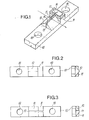
- the base shown in Figure 1 comprises a single piece metal support 10 having a prismatic portion 12 formed by two planes also inclined relative to the plane of symmetry of the assembly. This prismatic part is pierced with a slot 13 formed in the plane of symmetry. A metal strip 14 is brazed in the slot, this strip having a polished upper field intended to receive a laser chip 15. The length of this chip is equal to the thickness of the strip. The laser radiation is therefore directed transversely.
- the base further comprises a base 11 on which is brazed an interconnection plate 16 of parallelepiped shape.
- the support may include fixing holes 18.
- the prismatic shape 12 releases the laser chip and the mirrors without harming the thermal contact which remains established over the entire base of the laser chip.
- the manufacturing process for such a base can include the following operations, in which is only an example of implementation.
- the support is obtained by milling and rectifying a round or drawn copper, for example of the annealed Cu type.
- the part shown in FIG. 2 is obtained, with its base 11 and its prismatic part 12.
- the slot 13 is obtained by sawing on a milling machine using a width milling cutter such that the desired width is obtained in a single pass. This is equal to the thickness of the strip to be mounted, increased from 30 to 40 ⁇ .Lm.
- Deburring is then carried out, followed by degreasing with chlorinated or fluorinated solvents in an ultrasonic tank.
- the strip is then preferably made of annealed copper, as for the support.
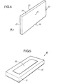
- the material is supplied with sheets from which strips 2.5 mm wide and about 250 mm long are drawn. Each strip is passed through a rolling mill to bring its thickness to that of the strip to ⁇ 1 ⁇ m. The strips coming out of the rolling are cut to a length of 4.5 mm using a saw mill. After cutting, the strips are cleaned using a chlorinated or fluorinated solvent. Each strip then undergoes rectification on three faces, referenced 23, 25, 26 in FIG. 4, the faces 21 and 22 remaining rough from rolling. The strips are then subject to polishing on their face 24 intended to receive the laser chip.
- the interconnection plate is shown in FIG. 5. It consists of a sintered alumina substrate 30 covered with a conductive layer 32 used for interconnection and produced by screen printing of a gold paste without glass. The underside used for fixing to the base of the support is covered with a layer 34 obtained using a silver-palladium paste. Several wafers can be screen-printed simultaneously and baked on an alumina substrate, which is then cut using laser beam machining equipment.
- the strip is fixed by soft soldering in the slot made in the support.
- the filler alloy is chosen according to its melting temperature and the thermal resistance characteristics requested from the base. For example, for resistance to 160 ° C., a 62.5% tin alloy, 36% lead, 1.5% silver can be used, the melting temperature of which is 179 ° C. For a resistance at 200 ° C., it is possible to use a 95% tin alloy 5% antimony whose melting temperature is 240 ° C.
- the lamella mounting operation comprises two phases: coating the faces of the slot with the filler metal, then brazing the lamella.
- the coating of the faces of the slot is carried out using a preform of the chosen filler alloy, which makes it possible to treat only the slot.
- the preform is engaged by centering it in the slot so that it is flush with the upper part.
- the support is brought to a temperature slightly higher than the melting temperature of the preform, for example by placing it on a hot plate.
- the preform melts by flowing over the sides and the bottom of the slot.
- a strip of stainless steel is passed through the slot, the thickness of which is equal to that of the slot minus 100 ⁇ m.
- a longitudinal back and forth movement is applied to the strip, which makes it possible to obtain a deposit without excess thickness.
- the flat part of the support to receive the interconnection plate is coated with the same alloy. The whole is cooled by placing the support on a good heat sink.
- the strip is engaged in the slot by centering it.
- the interconnection plate is placed in position on its support.
- the mounting support is brought to the melting temperature of the preform and pressure is applied to the ends of the strip allowing the latter to be brought into abutment at the bottom of the slot.
- the strip and the interconnection plate are brazed simultaneously.
- the part is cooled, then it is cleaned in a chlorinated solvent.
- the bases are then stored in a dehydrated enclosure.
- the assembled assembly can be subjected to a surface treatment by electrolytic deposits comprising a deposit of shiny nickel 0.5 to 1 ⁇ m thick, itself coated with a gold deposit of 0.4 at 0.6 ⁇ .Lm thick.
Description
La présente invention a pour objet une embase pour laser à semiconducteur et son procédé de fabrication.The subject of the present invention is a base for a semiconductor laser and its manufacturing process.
Une embase pour laser à semiconducteur est une pièce destinée à servir de support mécanique à la structure semiconductrice siège de l'effet laser, à permettre une dissipation de la chaleur dégagée dans cette structure et à faciliter les connexions électriques avec une source d'alimentation.A base for semiconductor laser is a part intended to serve as mechanical support for the semiconductor structure seat of the laser effect, to allow dissipation of the heat released in this structure and to facilitate electrical connections with a power source.
Du document <cJournal of Applied Physics, Vol. 46, No. 2, février 1975, pages 885-862, une embase pour laser à semiconducteur est connue, cette embase comprenant un support métallique monobloc présentant une partie prismatique formée par deux plans également inclinés par rapport à un plan de symétrie. La partie prismatique présentant un champ supérieur poli destiné à recevoir une puce laser dont la longueur est égale à l'épaisseur du champ supérieur poli.From the document <cJournal of Applied Physics, Vol. 46, No. 2, February 1975, pages 885-862, a base for a semiconductor laser is known, this base comprising a monobloc metal support having a prismatic part formed by two planes also inclined with respect to a plane of symmetry. The prismatic part having a polished upper field intended to receive a laser chip whose length is equal to the thickness of the polished upper field.
Du document «GB-A 2 050 896 une embase pour laser à semiconducteur est connue, cette embase comprenant un support métallique monobloc, sur lequel est brasée une plaquette d'interconnexion de forme parallélépipédique, constituée par un substrat isolant recouvert d'une couche métallique susceptible d'être reliée par une connexion à la puce laser.From the document “GB-A 2 050 896 a base for a semiconductor laser is known, this base comprising a monobloc metal support, on which is brazed an interconnection plate of parallelepiped shape, constituted by an insulating substrate covered with a metal layer likely to be connected by a connection to the laser chip.
Etant donné l'extrême sensibilité de lasers à semiconducteur, le problème de la réalisation d'une embase adéquate a toujours été au premier plan des préoccupations des spécialistes de ce domaine. En général, l'embase utilisée est constituée par un support métallique monobloc dont la face supérieure est polie et reçoit la puce laser. Mais une telle structure présente deux inconvénients:
- - la surface supérieure de l'embase se trouve être bombée après polissage, du fait de sa dimension importante, ce qui nuit à un bon contact thermique entre la puce et l'embase;
- - les miroirs du laser, qui encadrent la structure semiconductrice, sont très difficilement accessibles, une fois l'ensemble monté.
- - The upper surface of the base is curved after polishing, due to its large size, which affects good thermal contact between the chip and the base;
- - The laser mirrors, which frame the semiconductor structure, are very difficult to access, once the assembly is mounted.
La présente invention a justement pour but de remédier à ces inconvénients en proposant une embase pour laquelle la partie recevant la puce laser est étroite et ne présente pas de bombage et, qui, en outre, laisse accessibles les miroirs du laser.The object of the present invention is precisely to remedy these drawbacks by proposing a base for which the part receiving the laser chip is narrow and does not exhibit bending and, which, moreover, leaves the laser mirrors accessible.
Ce but est atteint, selon l'invention, par une embase comprenant un support métallique monobloc présentant une partie prismatique formée par deux plans également inclinés par rapport à un plan de symétrie, cette partie prismatique étant percée d'une fente pratiquée dans ce plan de symétrie, une lamelle métallique étant brasée dans la fente, cette lamelle présentant un champ supérieur poli destiné à recevoir une puce laser dont la longueur est égale à l'épaisseur de la lamelle, le support présentant en outre un socle plan sur lequel est brasé une plaquette d'interconnexion de forme parallélépipédique, cette plaquette étant constituée par un substrat isolant recouvert d'une couche métallique susceptible d'être reliée par une connexion à la puce laser.This object is achieved, according to the invention, by a base comprising a one-piece metal support having a prismatic part formed by two planes also inclined relative to a plane of symmetry, this prismatic part being pierced with a slot made in this plane of symmetry, a metal strip being brazed in the slot, this strip having a polished upper field intended to receive a laser chip whose length is equal to the thickness of the strip, the support further having a flat base on which a interconnection plate of parallelepiped shape, this plate being constituted by an insulating substrate covered with a metallic layer capable of being connected by a connection to the laser chip.
De préférence, le support et la lamelle sont en cuivre.Preferably, the support and the strip are made of copper.
De préférence encore, la plaquette d'interconnexion est constituée par un substrat en alumine frittée recouvert sur une face par une couche conductrice sérigraphiée à l'or, et sur l'autre face, (destinée à être en contact avec le socle) par une couche conductrice de la chaleur réalisée à l'aide d'une pâte argent-palladium.More preferably, the interconnection plate is constituted by a sintered alumina substrate covered on one side by a conductive layer screen printed with gold, and on the other side (intended to be in contact with the base) by a heat conducting layer produced using a silver-palladium paste.
La présente invention a également pour objet un procédé de fabrication de l'embase qui vient d'être définie. Ce procédé est caractérisé en ce qu'il comprend les opérations suivantes:
- - usinage d'un support métallique par fraisage et rectification pour former la partie prismatique et le socle,
- - sciage d'une fente dans la partie prismatique et dans le socle,
- - fabrication d'une lamelle par laminage d'une bande métallique, découpage à la longueur désirée, rectification sur trois champs et polissage du quatrième, devant recevoir la puce laser,
- - fabrication d'une plaquette d'interconnexion par sérigraphie d'une pâte métallique sur un substrat isolant,
- - introduction de la lamelle dans la fente, et mise en place de la plaquette d'interconnexion sur le socle,
- - brasage de la lamelle et de la plaquette.
- - machining of a metal support by milling and rectification to form the prismatic part and the base,
- - sawing a slot in the prismatic part and in the base,
- - manufacture of a strip by rolling a metal strip, cutting to the desired length, rectification on three fields and polishing of the fourth, to receive the laser chip,
- - manufacture of an interconnection plate by screen printing of a metallic paste on an insulating substrate,
- - introduction of the strip into the slot, and installation of the interconnection plate on the base,
- - brazing of the coverslip and the plate.
Les caractéristiques de l'invention apparaîtront mieux après la description qui suit, d'exemples de réalisation donnés à titre explicatif et nullement limitatif. Cette description se réfère à des dessins sur lesquels:
- - la fig. 1 représente une vue générale d'une embase conforme à l'invention,
- - la fig. 2 représente le support monobloc,
- - la fig. 3 représente le support après sciage,
- - la fig. 4 représente une lamelle,
- - la fig. 5 représente une plaquette d'interconnexion.
- - fig. 1 represents a general view of a base according to the invention,
- - fig. 2 represents the monobloc support,
- - fig. 3 represents the support after sawing,
- - fig. 4 represents a strip,
- - fig. 5 shows an interconnection plate.
L'embase représentée sur la figure 1 comprend un support métallique monobloc 10 présentant une partie prismatique 12 formée par deux plans également inclinés par rapport au plan de symétrie de l'ensemble. Cette partie prismatique est percée d'une fente 13 pratiquée dans le plan de symétrie. Une lamelle métallique 14 est brasée dans la fente, cette lamelle présentant un champ supérieur poli destiné à recevoir une puce laser 15. La longueur de cette puce est égale à l'épaisseur de la lamelle. Le rayonnement laser est donc dirigé transversalement. L'embase comprend encore un socle 11 sur lequel est brasée une plaquette d'interconnexion 16 de forme parallélépipédique. Le support peut comprendre des trous de fixation 18.The base shown in Figure 1 comprises a single
On conçoit que la forme prismatique 12 dégage la puce laser et les miroirs sans pour autant nuire au contact thermique qui reste établi sur la totalité de la base de la puce laser.It is understood that the
Le procédé de fabrication d'une telle embase peut comporter les opérations suivantes, dans ce qui n'est qu'un exemple de mise en oeuvre.The manufacturing process for such a base can include the following operations, in which is only an example of implementation.
Le support est obtenu par fraisage et rectification d'un rond ou d'un étiré de cuivre, par exemple de type Cu recuit. On obtient la pièce représentée sur la figure 2, avec son socle 11 et sa partie prismatique 12.The support is obtained by milling and rectifying a round or drawn copper, for example of the annealed Cu type. The part shown in FIG. 2 is obtained, with its
La fente 13 est obtenue par sciage sur fraiseuse à l'aide d'une fraise-scie de largeur telle qu'on obtienne en une seule passe la largeur souhaitée. Celle-ci est égale, à l'épaisseur de la lamelle à monter, augmentée de 30 à 40 ¡.Lm.The
Un ébavurage est ensuite effectué, suivi d'un dégraissage aux solvants chlorés ou fluorés dans un bac à ultrasons.Deburring is then carried out, followed by degreasing with chlorinated or fluorinated solvents in an ultrasonic tank.
La pièce obtenue est représentée sur la fig. 3.The part obtained is shown in FIG. 3.
La lamelle est ensuite réalisée de préférence en cuivre recuit, comme pour le support. La matière est approvisionnée en feuilles d'où sont tirées des bandes de largeur 2,5 mm et d'environ 250 mm de longueur. Chaque bande est passée dans un laminoir pour amener son épaisseur à celle de la lamelle à ± 1 µm. Les bandes sortant de laminage sont découpées à une longueur de 4,5 mm à l'aide d'une fraise-scie. Après découpe, les lamelles sont nettoyées à l'aide d'un solvant chloré ou fluoré. Chaque lamelle subit alors une rectification sur trois faces, référencées 23, 25, 26 sur la figure 4, les faces 21 et 22 restant brutes de laminage. Les lamelles font ensuite l'objet d'un polissage sur leur face 24 destinée à recevoir la puce laser. Pour cette opération de polissage, un bloc de lamelles est maintenu dans un montage spécial possédant deux flasques venant en appui sur les faces latérales, respectivement 21 et 22, des deux lamelles d'extrémité du bloc. Après polissage du bloc, les lamelles sont séparées les unes des autres. Cette manière de procéder permet d'obtenir une face 24 poli-miroir sans faire tomber les bords. Seuls les bords du montage enserrant les lamelles présentent un bord abattu. La plaquette d'interconnexion est représentée sur la figure 5. Elle est constituée d'un substrat 30 en alumine frittée recouvert d'une couche conductrice 32 servant à l'interconnexion et réalisée par sérigraphie d'une pâte à l'or sans verre. La face inférieure servant à la fixation sur le socle du support est recouverte d'une couche 34 obtenue à l'aide d'une pâte argent-palladium. Plusieurs plaquettes peuvent être sérigraphiées simultanément et cuites sur un substrat d'alumine, lequel est ensuite découpé à l'aide d'un équipement d'usinage par faisceau laser.The strip is then preferably made of annealed copper, as for the support. The material is supplied with sheets from which strips 2.5 mm wide and about 250 mm long are drawn. Each strip is passed through a rolling mill to bring its thickness to that of the strip to ± 1 µm. The strips coming out of the rolling are cut to a length of 4.5 mm using a saw mill. After cutting, the strips are cleaned using a chlorinated or fluorinated solvent. Each strip then undergoes rectification on three faces, referenced 23, 25, 26 in FIG. 4, the
La lamelle est fixée par brasage tendre dans la fente pratiquée dans le support. L'alliage d'apport est choisi en fonction de sa température de fusion et des caractéristiques de tenue thermique demandée à l'embase. Par exemple pour une tenue à 160°C, on peut utiliser un alliage étain 62,5%, plomb 36%, argent 1,5% dont la température de fusion est 179°C. Pour une tenue à 200°C, on peut utiliser un alliage étain 95% antimoine 5% dont la température de fusion est 240°C.The strip is fixed by soft soldering in the slot made in the support. The filler alloy is chosen according to its melting temperature and the thermal resistance characteristics requested from the base. For example, for resistance to 160 ° C., a 62.5% tin alloy, 36% lead, 1.5% silver can be used, the melting temperature of which is 179 ° C. For a resistance at 200 ° C., it is possible to use a 95% tin alloy 5% antimony whose melting temperature is 240 ° C.
L'opération de montage de la lamelle comprend deux phases: revêtement des faces de la fente par le métal d'apport, puis brasage de la lamelle.The lamella mounting operation comprises two phases: coating the faces of the slot with the filler metal, then brazing the lamella.
Le revêtement des faces de la fente est effectué en utilisant une préforme de l'alliage d'apport choisi, ce qui permet de ne traiter que la fente.The coating of the faces of the slot is carried out using a preform of the chosen filler alloy, which makes it possible to treat only the slot.
La mise en oeuvre de cette méthode se fait de la manière suivante: après dégraissage aux solvants chlorés ou fluorés, on décape le support de la figure 3 dans une solution à 5% d'acide chlorhydrique. On prépare une préforme en alliage d'apport dont les dimensions sont:
- longueur = longueur de la fente
- épaisseur = largeur de la fente
- largeur = entre 400 est 600 µm.
- length = slot length
- thickness = slit width
- width = between 400 and 600 µm.
On engage la préforme en la centrant dans la fente de manière qu'elle affleure à la partie supérieure. On porte le support à une température légèrement supérieure à la température de fusion de la préforme, par exemple en le posant sur une plaque chauffante. La préforme fond en s'écoulant sur les côtés et le fond de la fente. Pendant que l'alliage est en fusion, on passe dans la fente un feuillard d'acier inoxydable dont l'épaisseur est égale à celle de la fente moins 100 ¡.Lm. Un mouvement longitudinal de va et vient est appliqué au feuillard, ce qui permet d'obtenir un dépôt sans surépaisseur. On revêt du même alliage la partie plane du support devant recevoir la plaquette d'interconnexion. On refroidit l'ensemble en plaçant le support sur un bon dissipateur thermique.The preform is engaged by centering it in the slot so that it is flush with the upper part. The support is brought to a temperature slightly higher than the melting temperature of the preform, for example by placing it on a hot plate. The preform melts by flowing over the sides and the bottom of the slot. While the alloy is in fusion, a strip of stainless steel is passed through the slot, the thickness of which is equal to that of the slot minus 100 µm. A longitudinal back and forth movement is applied to the strip, which makes it possible to obtain a deposit without excess thickness. The flat part of the support to receive the interconnection plate is coated with the same alloy. The whole is cooled by placing the support on a good heat sink.
A partir d'un support ainsi préparé, on introduit dans la fente une préforme d'alliage de même nature que celle qui a été utilisée précédemment, mais dont les dimensions sont:
- longueur: 2 mm
- largeur: 0,6 mm
- épaisseur: celle de la largeur de la fente moins 100 µm.
- length: 2 mm
- width: 0.6mm
- thickness: that of the width of the slit minus 100 µm.
On engage la lamelle dans la fente en la centrant. On place en position sur son support la plaquette d'interconnexion. On porte le support de montage à la température de fusion de la préforme et on effectue sur les extrémités de la lamelle une pression permettant d'amener celle-ci en butée au fond de la fente.The strip is engaged in the slot by centering it. The interconnection plate is placed in position on its support. The mounting support is brought to the melting temperature of the preform and pressure is applied to the ends of the strip allowing the latter to be brought into abutment at the bottom of the slot.
Au cours de cette opération, la lamelle et la plaquette d'interconnexion se trouvent brasées simultanément. On refroidit la pièce, puis on nettoie celle-ci dans un solvant chloré. Les embases sont alors stockées en enceinte déshydratée.During this operation, the strip and the interconnection plate are brazed simultaneously. The part is cooled, then it is cleaned in a chlorinated solvent. The bases are then stored in a dehydrated enclosure.
L'ensemble monté peut faire l'objet d'un traitement de surface par dépôts électrolytiques comprenant un dépôt de nickel brillant de 0,5 à 1 µm d'épaisseur, revêtu lui-même d'un dépôt d'or de 0,4 à 0,6 ¡.Lm d'épaisseur.The assembled assembly can be subjected to a surface treatment by electrolytic deposits comprising a deposit of shiny nickel 0.5 to 1 μm thick, itself coated with a gold deposit of 0.4 at 0.6 ¡.Lm thick.
Claims (8)
Applications Claiming Priority (2)
| Application Number | Priority Date | Filing Date | Title |
|---|---|---|---|
| FR8214042 | 1982-08-12 | ||
| FR8214042A FR2531819A1 (en) | 1982-08-12 | 1982-08-12 | EMBASE FOR SEMICONDUCTOR LASER AND METHOD FOR MANUFACTURING THE SAME |
Publications (3)
| Publication Number | Publication Date |
|---|---|
| EP0101374A2 EP0101374A2 (en) | 1984-02-22 |
| EP0101374A3 EP0101374A3 (en) | 1984-04-11 |
| EP0101374B1 true EP0101374B1 (en) | 1987-01-07 |
Family
ID=9276828
Family Applications (1)
| Application Number | Title | Priority Date | Filing Date |
|---|---|---|---|
| EP83401626A Expired EP0101374B1 (en) | 1982-08-12 | 1983-08-08 | Semiconductor laser substrate and process for its production |
Country Status (6)
| Country | Link |
|---|---|
| US (1) | US4584688A (en) |
| EP (1) | EP0101374B1 (en) |
| JP (1) | JPS5948978A (en) |
| CA (1) | CA1209235A (en) |
| DE (1) | DE3369033D1 (en) |
| FR (1) | FR2531819A1 (en) |
Families Citing this family (8)
| Publication number | Priority date | Publication date | Assignee | Title |
|---|---|---|---|---|
| US4688076A (en) * | 1983-04-22 | 1987-08-18 | The Charles Stark Draper Laboratory, Inc. | Noise reducing heat sink for semiconductor laser diodes |
| FR2550023B1 (en) * | 1983-07-25 | 1987-03-27 | Auffret Rene | INFRARED LIGHT SOURCE COMPRISING A SEMICONDUCTOR LASER ASSOCIATED WITH MEANS OF MODE SELECTION AND POWER SUPPLY |
| US4797728A (en) * | 1986-07-16 | 1989-01-10 | General Electric Company | Semiconductor device assembly and method of making same |
| US4820659A (en) * | 1986-07-16 | 1989-04-11 | General Electric Company | Method of making a semiconductor device assembly |
| JPH0750813B2 (en) * | 1988-05-23 | 1995-05-31 | 三菱電機株式会社 | Submount for semiconductor laser device |
| US6869231B2 (en) * | 2002-05-01 | 2005-03-22 | Jds Uniphase Corporation | Transmitters, receivers, and transceivers including an optical bench |
| US7061949B1 (en) * | 2002-08-16 | 2006-06-13 | Jds Uniphase Corporation | Methods, apparatus, and systems with semiconductor laser packaging for high modulation bandwidth |
| US20060038302A1 (en) * | 2004-08-19 | 2006-02-23 | Kejun Zeng | Thermal fatigue resistant tin-lead-silver solder |
Family Cites Families (5)
| Publication number | Priority date | Publication date | Assignee | Title |
|---|---|---|---|---|
| JPS5314588A (en) * | 1976-07-26 | 1978-02-09 | Mitsubishi Electric Corp | Optical device |
| JPS56104485A (en) * | 1980-01-23 | 1981-08-20 | Canon Inc | Semiconductor laser device |
| JPS55148483A (en) * | 1979-05-08 | 1980-11-19 | Canon Inc | Semiconductor laser device |
| NL180365C (en) * | 1979-06-11 | 1987-02-02 | Philips Nv | METHOD FOR MANUFACTURING SEMICONDUCTOR COOLING BLOCKS AND SEMICONDUCTOR LASER CONTAINING A COOLING BLOCK MANUFACTURED BY THIS PROCESS. |
| NL181963C (en) * | 1979-06-26 | 1987-12-01 | Philips Nv | SEMICONDUCTOR LASER DEVICE. |
-
1982
- 1982-08-12 FR FR8214042A patent/FR2531819A1/en active Granted
-
1983
- 1983-08-08 DE DE8383401626T patent/DE3369033D1/en not_active Expired
- 1983-08-08 EP EP83401626A patent/EP0101374B1/en not_active Expired
- 1983-08-08 CA CA000434081A patent/CA1209235A/en not_active Expired
- 1983-08-08 US US06/521,106 patent/US4584688A/en not_active Expired - Fee Related
- 1983-08-11 JP JP58145782A patent/JPS5948978A/en active Pending
Non-Patent Citations (1)
| Title |
|---|
| JOURNAL OF APPLIED PHYSICS, vol. 46, no. 2, février 1975, American Institute of Physics, NEW YORK (US), W.B. JOYCE et al.: "Thermal resistance of heterostructure lasers", pages 855-862 * |
Also Published As
| Publication number | Publication date |
|---|---|
| EP0101374A2 (en) | 1984-02-22 |
| US4584688A (en) | 1986-04-22 |
| CA1209235A (en) | 1986-08-05 |
| FR2531819B1 (en) | 1985-03-08 |
| JPS5948978A (en) | 1984-03-21 |
| EP0101374A3 (en) | 1984-04-11 |
| FR2531819A1 (en) | 1984-02-17 |
| DE3369033D1 (en) | 1987-02-12 |
Similar Documents
| Publication | Publication Date | Title |
|---|---|---|
| US5593901A (en) | Monolithic series and parallel connected photovoltaic module | |
| CA1297595C (en) | Printed circuit with thermal dissipator | |
| JP4565650B2 (en) | ELECTRODE WIRE, ITS MANUFACTURING METHOD, AND SOLAR CELL HAVING CONNECTION LEAD FORMED BY THE ELECTRODE WIRE | |
| FR2501415A1 (en) | HEAT AND ELECTRIC CONDUCTING BASE FOR RECEIVING SEMICONDUCTOR ELEMENT AND METHOD FOR MANUFACTURING THE SAME | |
| US20050139249A1 (en) | Thermoelectric module and a method of manufacturing the same | |
| EP0803949B1 (en) | Laser diode device | |
| WO1998028801A1 (en) | Thermoelectric piece and process of making the same | |
| EP0101374B1 (en) | Semiconductor laser substrate and process for its production | |
| CA2422471A1 (en) | Thermoelectric element and process for the manufacture thereof as well as process and device for separating and transferring layer materials for manufacturing such a thermoelectric element | |
| FR2646018A1 (en) | SEMICONDUCTOR DEVICE AND MANUFACTURING METHOD THEREOF | |
| US4425195A (en) | Method of fabricating a diamond heat sink | |
| EP1005083B1 (en) | High-power electronic device comprising cooling system | |
| EP0021894B1 (en) | Method and device for interconnecting electronic components | |
| EP0228119B1 (en) | Centering device for the realization of the pin insertion of a multipin case | |
| EP0178977A1 (en) | Semiconductor component mounted in a plastic housing, and method for its manufacture | |
| FR2826541A1 (en) | IMPROVEMENTS ON THE STRUCTURE OF A GRAPHITE RESISTANCE OVEN | |
| EP0038243B1 (en) | Profiled metallic bar for producing a conductive element, method for producing the element, and the element so produced | |
| EP1333481B1 (en) | Process for soldering leads on substrates | |
| FR2790905A1 (en) | POWER ELECTRICAL COMPONENT MOUNTED BY BRAZING ON A SUPPORT AND ASSEMBLY METHOD THEREFOR | |
| FR2601818A1 (en) | MOUNTING OF A SEMICONDUCTOR DEVICE ON A BASE | |
| FR2724495A1 (en) | BATTERY OF LASER DIODE BARS, AND METHOD OF ASSEMBLING THE SAME | |
| FR2572852A1 (en) | Semiconductor component with two main electrodes | |
| EP0242667B1 (en) | Soldering tool for electronic devices | |
| EP0117804A1 (en) | Manufacturing method of a microwave cavity, and cavity obtained thereby | |
| FR2571547A1 (en) | Hybrid circuit which can be transferred to a support containing a high-density interconnection network |
Legal Events
| Date | Code | Title | Description |
|---|---|---|---|
| PUAI | Public reference made under article 153(3) epc to a published international application that has entered the european phase |
Free format text: ORIGINAL CODE: 0009012 |
|
| PUAL | Search report despatched |
Free format text: ORIGINAL CODE: 0009013 |
|
| AK | Designated contracting states |
Designated state(s): BE CH DE GB IT LI NL SE |
|
| AK | Designated contracting states |
Designated state(s): BE CH DE GB IT LI NL SE |
|
| 17P | Request for examination filed |
Effective date: 19840921 |
|
| 17Q | First examination report despatched |
Effective date: 19860307 |
|
| GRAA | (expected) grant |
Free format text: ORIGINAL CODE: 0009210 |
|
| AK | Designated contracting states |
Kind code of ref document: B1 Designated state(s): BE CH DE GB IT LI NL SE |
|
| REF | Corresponds to: |
Ref document number: 3369033 Country of ref document: DE Date of ref document: 19870212 |
|
| ITF | It: translation for a ep patent filed |
Owner name: JACOBACCI & PERANI S.P.A. |
|
| PG25 | Lapsed in a contracting state [announced via postgrant information from national office to epo] |
Ref country code: SE Effective date: 19870809 |
|
| PG25 | Lapsed in a contracting state [announced via postgrant information from national office to epo] |
Ref country code: LI Effective date: 19870831 Ref country code: CH Effective date: 19870831 |
|
| PLBE | No opposition filed within time limit |
Free format text: ORIGINAL CODE: 0009261 |
|
| STAA | Information on the status of an ep patent application or granted ep patent |
Free format text: STATUS: NO OPPOSITION FILED WITHIN TIME LIMIT |
|
| 26N | No opposition filed | ||
| BERE | Be: lapsed |
Owner name: SIMON JEAN CLAUDE Effective date: 19870831 Owner name: LE ROUZIC JEAN Effective date: 19870831 Owner name: DEMEURE LOIC Effective date: 19870831 |
|
| PG25 | Lapsed in a contracting state [announced via postgrant information from national office to epo] |
Ref country code: NL Effective date: 19880301 |
|
| NLV4 | Nl: lapsed or anulled due to non-payment of the annual fee | ||
| REG | Reference to a national code |
Ref country code: CH Ref legal event code: PL |
|
| GBPC | Gb: european patent ceased through non-payment of renewal fee | ||
| PG25 | Lapsed in a contracting state [announced via postgrant information from national office to epo] |
Ref country code: GB Free format text: LAPSE BECAUSE OF NON-PAYMENT OF DUE FEES Effective date: 19881122 |
|
| PG25 | Lapsed in a contracting state [announced via postgrant information from national office to epo] |
Ref country code: DE Effective date: 19890503 |
|
| PG25 | Lapsed in a contracting state [announced via postgrant information from national office to epo] |
Ref country code: BE Effective date: 19890831 |
|
| EUG | Se: european patent has lapsed |
Ref document number: 83401626.3 Effective date: 19880711 |