EP0100213B1 - VLSI-Chip aus Galliumarsenid - Google Patents
VLSI-Chip aus Galliumarsenid Download PDFInfo
- Publication number
- EP0100213B1 EP0100213B1 EP83304252A EP83304252A EP0100213B1 EP 0100213 B1 EP0100213 B1 EP 0100213B1 EP 83304252 A EP83304252 A EP 83304252A EP 83304252 A EP83304252 A EP 83304252A EP 0100213 B1 EP0100213 B1 EP 0100213B1
- Authority
- EP
- European Patent Office
- Prior art keywords
- source
- voltage
- transistor
- gate
- region
- Prior art date
- Legal status (The legal status is an assumption and is not a legal conclusion. Google has not performed a legal analysis and makes no representation as to the accuracy of the status listed.)
- Expired
Links
Images


Classifications
-
- H—ELECTRICITY
- H10—SEMICONDUCTOR DEVICES; ELECTRIC SOLID-STATE DEVICES NOT OTHERWISE PROVIDED FOR
- H10D—INORGANIC ELECTRIC SEMICONDUCTOR DEVICES
- H10D84/00—Integrated devices formed in or on semiconductor substrates that comprise only semiconducting layers, e.g. on Si wafers or on GaAs-on-Si wafers
- H10D84/01—Manufacture or treatment
-
- H—ELECTRICITY
- H10—SEMICONDUCTOR DEVICES; ELECTRIC SOLID-STATE DEVICES NOT OTHERWISE PROVIDED FOR
- H10D—INORGANIC ELECTRIC SEMICONDUCTOR DEVICES
- H10D30/00—Field-effect transistors [FET]
- H10D30/80—FETs having rectifying junction gate electrodes
- H10D30/87—FETs having Schottky gate electrodes, e.g. metal-semiconductor FETs [MESFET]
-
- H—ELECTRICITY
- H10—SEMICONDUCTOR DEVICES; ELECTRIC SOLID-STATE DEVICES NOT OTHERWISE PROVIDED FOR
- H10D—INORGANIC ELECTRIC SEMICONDUCTOR DEVICES
- H10D62/00—Semiconductor bodies, or regions thereof, of devices having potential barriers
- H10D62/10—Shapes, relative sizes or dispositions of the regions of the semiconductor bodies; Shapes of the semiconductor bodies
- H10D62/17—Semiconductor regions connected to electrodes not carrying current to be rectified, amplified or switched, e.g. channel regions
- H10D62/213—Channel regions of field-effect devices
- H10D62/221—Channel regions of field-effect devices of FETs
-
- H—ELECTRICITY
- H10—SEMICONDUCTOR DEVICES; ELECTRIC SOLID-STATE DEVICES NOT OTHERWISE PROVIDED FOR
- H10D—INORGANIC ELECTRIC SEMICONDUCTOR DEVICES
- H10D84/00—Integrated devices formed in or on semiconductor substrates that comprise only semiconducting layers, e.g. on Si wafers or on GaAs-on-Si wafers
- H10D84/01—Manufacture or treatment
- H10D84/02—Manufacture or treatment characterised by using material-based technologies
- H10D84/05—Manufacture or treatment characterised by using material-based technologies using Group III-V technology
Definitions
- the invention is concerned with gallium arsenide VLSI chips carrying electronic circuits such as are used in digital equipment, for example, computers.
- GaAs output drives and buffer amplifiers could be made of depletion mode devices.
- GaAs depletion mode devices are normally ON, and a negative voltage is applied between the gate and the source so that the electric field in the channel region is enlarged to pinch off or deplete the current flow in the channel.
- the implant regions under the source and drain have a different N dopant concentration and/or a different dopant depth from the channel implant region under the gate. This permits control of the threshold voltage and breakdown voltage independent of parasitic source and drain contact resistances.
- the source and drain implant regions fo a MESFET device with concentration of the implant dopants having 10 18 atoms per cubic centimeter.
- the channel implant region under the gate with concentrations of implant dopants having only 10 17 atoms per cubic centimeter.
- the reason for employing the smaller concentration of implant dopants in the channel region under the gate is to permit the construction of MESFET devices with low threshold voltages and to increase the breakdown voltage to provide operable devices for digital operations microwave operations and millimeter wavelength intergrated circuit operations.
- GaAs depletion mode MESFET devices are useful in high-speed low power digital integrated circuit applications. However, such devices are not well suited for high power applications, or for high density applications, such as the type embodied in very large scale integrated circuits.
- the object of the present invention is to provide an improved MESFET buffer amplifier device on a gallium arsenide VLSI chip capable of giving an increased power output and improved packing density with the attendant advantages of low switching time and improved performance, and which is capable of being manufactured by known methods.
- the chip of the invention makes use of a nord type of depletion mode field effect transistor of the MESFET type having a uniform depth implant region extending below source, gate, and drain electrodes, and having a higher than usual concentration of at least 5.1017 Atlcm3 of implanted atoms per cubic centimeter, connected to a low voltage signal source in such a way as to function as a source follower amplifier.
- FIG. 1 is a block diagram employed to explain the problem presented in prior art depletion mode MESFET devices.
- An input signal waveform initiated at time TO is applied to a low signal source 12, such as low power logic ciruitry, to produce a low power signal on line 13 at time T1.
- a buffer amplifier 14 is applied to a buffer amplifier 14 to produce an output driving signal on output line 15 at time T2.
- the load to be driven by such buffer amplifier is a large capacitive load 16, which presents a problem, in that the buffer amplifier 14 must be made large in order to drive the capacitive load 16 at high speed, as a result of which it presents a much larger input and output capacitance to the circuit. Since the output capacitance of the buffer amplifier 14 is large, the buffer amplifier itself slows down its speed of operation.
- the typical prior art solution is to greatly increase the size and power of the buffer amplifier 14, and this prevents this prior art solution from being incorporated into very large scale integrated circuits. Further, employing even a moderately increased size buffer amplifier causes lengthening of the interconnect signal lines thereby further slowing operation.
- FIG. 2 is a schematic drawing in enlarged cross-section showing the construction of a typical prior art GaAs metal semiconductor field effect transistor (MESFET).
- the GaAs semi-insulating substrate 17 is employed as a host for further processing to produce the MESFET device.
- a source implant region 18 is provided with a high N+ dopant concentration, such as silicon, to provide a base for good ohmic contact for the source terminal 19.
- the N+ dopant concentration is of the order of 10 18 atoms per cubic centimeter and the typical depth is approximatley one thousand to two thousand angstroms.
- a similar drain implant region 21 is provided with a high concentration of N+ dopant, such as silicon, and is also adapted to provide good ohmic contact for the drain terminal 22.
- the channel implant region 23 between the implant regions 18 and 21 is provided with a low concentration N- dopant.
- the N- dopant is typically silicon.
- the channel implant region 23 is made more shallow than the source and drain implant regions, typically between eight hundred an sixteen hundred angstoms thick.
- the dopant concentration in the channel implant region is typically 10 17 atoms per cubic centimeter.
- the active channel resistance 26 shown in phantom lines represents the resistance in the channel which is under the direct control of the gate terminal 24 and its associated depletion region 28.
- the source terminal 19 is grounded.
- the depletion region 28 under the gate terminal 24 is very close to its minimum depth.
- the minimum depletion region 28 allows maximum current flow from the drain terminal 22 to the source terminal 19 via the channel region 23.
- the depletion region 28 under the gate 24 pinches off the channel region 23 so as to substantially shut off the current flow between the drain 22 and the source 19. Accordingly, voltages applied to the gate 24 may effect switching operation of the device by turning the device ON and OFF.
- An independent N+ region is shown on the substrate 17 with a negative voltage terminal 31, representing the N+ region of the source of an adjacent device.
- the phantom region 32 at the back of channel region 23 is exaggerated to show that there is a shallow depeletion region inherently present.
- Connecting the interface junction 32 and the independent region 29 is an electrical path 33 indicated by the lines 33, resistor 34 and capacitor 35.
- the depletion region 32 formed at the back of the channel 23 may severely affect switching performance and may also affect functioning of the logic elements. In the example shown, it is obvious that the depletion region formed at the iterface junction 32 diminishes the current in the channel region 23.
- the effect of the elements 33, 34 and 35 on a device is referred to in this art as the back-gate effect.
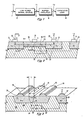
- FIG. 3 isa schematic enlarged cross-section of the construction of a GaAs metal semiconductor field effect transistor (MESFET) as used in the present invention.
- a semi-insulating GaAs host substrate 36 has a uniform depth N+ source, gate and drain implant region 37.
- the N+ implant region 37 has a silicon dopant concentration of approximately 1018 atoms per cubic centimetre. It will be understood that those skilled in this art may employ different dopants, different concentration and different dopant depths to optimise the structure and to provide a very high N+ concentration under the source, gate and drain. For typical applications, the silicon dopant concentration may be on the order of five times 10 17 to five times 10" atoms per cubic centimeter.
- the ohmic contact 38 is typically made from gold- nickle-germanium deposited and is alloyed to the implant region 37.
- the source terminal 39 is typically made from titanium-gold deposited on the ohmic contact region 38.
- a Schottky diode gate terminal 41 is deposited on the implant region 37 to provide the gate terminal for the device.
- the gate terminal is shown having a length "L” and a width "W” which will be employed to explain the enhanced performance achieved by the present invention. Below the gate terminal 41 is shown in phantom lines a first depletion region 42 and a second depletion region 43 typical of the ON and OFF conditions.
- An ohmic contact 44 for the drain terminal 45 is provided on the N+ region 37.
- the ohmic contact and the drain terminal may be made of the same materials as the source ohmic contact and source terminal.
- An independent N+ region 29' is shown, with a negative voltage terminal 31' similar to those in Figure 2.
- the N+ region 29' is shown connected to the back 46 of the implant region 37. Even though there is a small depletion region at the back 46 of implant region 37, it is so small that it is negligible because of the very high N+ dopant concentration of the implant region 37. Accordingly, the parasitic resistance 34', parasitic capacitance 35' and the conductive line 33' connecting the independent region 29' and the back 46 of the implant region 37 have only a very mimimal effect on the performance of the present invention device.
- the depth of the depletion region at the back of the implant region 37 is a function of the square root of the dopant concentration in the channel region.
- the dopant concentration is of an order of magnitude higher than the dopant concentration employed in the typical prior art device shown in Figure 2, there is a reduction in the back depletion region depth of about three to one.
- the input capacitance of the device is also proportional to the square root of the dopant concentration in the implant region 37, which has been explained as being of the order of magnitude 10" atoms per cubic centimeter.
- the transconductance of the device of Figure 3 is proportional to W/L times the square root of the dopant concentration in the implant region 37.
- Figure 4 shows the performance characteristics of the depletion mode MESFET device for different dopant concentrations.
- Column 1 of Figure 4 shows the dopant concentration (N d ) for various concentrations of operable MESFET devices.
- Column 2 shows the normalised transconductance which is a figure of merit gm divided by the input capacitance C.
- Column 3 is the normallsed gate area which is a function of the width W of gate 41.
- Column 4 is the normalised power, which for purposes of this explanation is maintained constant, to better compare different devices.
- Column 5 shows the normalised input capacitance which is proportional to the area of the gate terminal 41 and the square root of the dopant concentration of the region 37.
- Row 1 illustrates that when the dopant concentration is five times 10 16 , the transconductance divided by input capacitance (figure of merit) is unity and the normalised area is very large for the assumed normalised power. Further, the normalised input capacitance is vey high.
- Row 2 shows a typical dopant conentration of the N- region of 10".
- the normalised transconductance is unity, the normalised area, the normalised power and normalised input capacitance is also made unity for purposes of comparison to other channel dopants concentrations.
- the dopant concentration is increased from three times 10" shown in Row 3, to five times 10 17 in Row 4, to the present preferred embodiment of 10" shown in Row 5, the normalised area for the same device power decreases by a factor of one hundred to one.
- the normalised input capacitance also decreases by a factor of greater than thirty to one.
- the present invention can easily be incorporated into very large scale integrated circuits because of its substantial packing density improvement for a fixed or normalised power.
- Those skilled in this art will understand that by having a packing density by two orders of magnitude greater, that the interconnect lines and associated capacitance of the interconnect lines of the adjacent devices are substantially reduced and the speed of operation of the devices will be substantially enhanced or increased.
- FIG. 5 shows a preferred embodiment of the invention employing two of the improved devices shown in Figure 3.
- the low power GaAs input signal source 12 provides a low level voltage of -1.7 volts and a high level voltage of -0.3 volts.
- the output signal on line 13 is applied to the level shifting diodes 47 and 48 which drop the voltage 0.7 volts across each diode.
- the prior art type depletion mode current source pull-down transistor T1 serves as a current path for the level shifting diodes 47, 48 to the power supply of -5.2 volts. T1 stays normally ON.
- the level shifted voltage on line 49 is applied to the gate of the new and improved depletion mode buffer amplifier T2, which is identical in all respects to the current source pull-down transistor T3.
- the typical threshold voltage for the prior art type device T1 is approximately -1.0 volt and the threshold voltage for the new and improved devices T2 and T3 is approximately -20 volts.
- the level shifted voltage signals on line 49 are approximately -3.1 volts to -1.7 volts.
- the transistors T2 and T3 are designed to be in the always ON condition.
- the drain of transistor T2 is shown connected to ground.
- the voltage signal being applied at the gate of transistor T2 appears at the source of transistor T2 and at the output node 51 of the buffer amplifier.
- the buffer amplifier transistor T2 is operating as a source follower transistor and is also operating as a linear amplifier. In the digital mode of operation, transistor T2 is operated in one of the two distinct voltage states representative of the input. However, the circuit can be operated as a linear amplifier, in which case the input voltage will appear at the output node 51. When operated as a linear amplifier, the range of voltages being applied to the input gate of transistor T2 on line 49 may be expanded.
- the current 11 flowing through transistor T2 is approximatley equal to the current 13 flowing through the constant current source transistor T3 because the current 12 flowing in output line 15 is very small in comparison to the current 11. Since the transistors T2 and T3 are identical in all respects, the gate to source voltages across transistor T2 must be equal to the gate to source voltage across transisitor T3, which is zero. This results in the before-mentioned voltage follower action. The voltage being applied on line 49 to the gate of transistor T2 appears substantially unchanged at the output node 51.
- the load 16 is shown as comprising a load capacitor 52 and a load resistor 53, it will be understood that it could comprise a number of parallel loads in a fan-out configuration.
- the buffer amplifier may be operated at standard GaAs voltage levels without the requirement for a -20 volt power source, because the buffer amplifier T2 is being operated in the linear mode of operation and does not require the high power supply voltage which would be required if the transistor were used as a power switch.
- Figure 6 shows the transfer characteristics of the buffer amplifier shown in Figure 5.
- the voltage is stepped down by the diodes 47, 48 and appears at the gate of transistor T2 on line 49 and on line 15 as being 1.4 volts lower or -3.1 volts.
- the point 54 on the transfer curve 55 indicates this point.
- the high level voltage signal of -0.3 volts is applied to the input line 13, it appears at the gate of transistor T2 on line 49 and on line 15 as a -1.7 volt signal.
- This point is shown on the transfer characteristic curve as point 56.
- the transfer characteristic of voltage IN versus voltage OUT is shown being extended to approximately -4 volts at the output.
- the power supply voltage in the preferred embodiment buffer amplifier circuit of Figure 5 is only -5.2 volts and when a much higher power supply voltage is applied, the voltage characteristic curve 55 may be extended.
- Figure 7 shows a set of propagation delay curves. Refer also to Figure 1 for the explanation of the propagation delay in Figure 7.
- the input voltage signal on line 11 of Figure 1 is shown as waveform A which rises from the low level voltage (V Low ) to the high level voltage (V HIGH ) and extends to the right.
- Output waveform B on line 13 is shown starting at the high level voltage (V HIGH ) until it reaches the point 57. It then makes a downward transition until it reaches the low level voltage (V Low ) and there it extends to the right.
- the transition point 58 of waveform A is half-way between the high level and the low level voltages.
- the transition point of the waveform is indicated by the centre line 59.
- the half-way point 58 is indicative of the start of transition time TO on input line 11.
- the output waveform B starts from its high voltage level and reaches its midway switching point 61 very rapidly as shown by the time delay T1 new.
- an input-output waveform C of a typical prior art amplifier is shown starting from the high voltage until it reaches the same point 57. It then follows the phantom transition line of waveform C through the midway switching point 60 until it reaches the low level voltage and then extends outward to the right.
- the switching time T1 old for the low power signal source is substantially greater than the T1 new switching time when the present invention buffer amplified is employed.
- One of the reasons that the switching time delay has been substantially reduced is because the devices on the chip have been made much smaller, by an order of thirty to one hundred times. This size reduction substantially reduces the input capacitance, which allows the input power signal source to drive the buffer amplifier faster.
- Waveform D shows the output voltage waveform on line 15 employing the new buffer amplifier of Figure 5.
- the output voltage starts at the same high level as waveform B and stays high until it reaches the point 62 where it starts its transition to the low voltage condition.
- Waveform E shows the output voltage on line 15 for the prior art buffer amplifier. The voltage starts at the high voltage condition and proceeds to point 63 before it starts its downward transition to the low voltage condition (V Low ).
- the half-way point 64 on waveform D occurs before the half-way point 65 on waveform E.
- the same voltage levels and approximately the same amount of circuit power is being dissipated using the new buffer amplifier as was employed using the prior art buffer amplifier.
- the important feature of the present invention is that the new buffer amplifier only requires one thirtieth to one hundredth the area required by the prior art buffer amplifier to accomplish at least the same speed-power performance characteristic.
- additional speed enhancement it may be obtained by increasing the area of the buffer amplifier device, thus, producing faster transition times.
- the Figure 7 illustration has been designed to show that a very large area enhancement can be achieved while maintaining the same power and driving at a slightly faster switching speed.
- the same buffer amplifier may be used as a linear amplifier.
- the input voltage range of the linear amplifier may be extended by increasing the power supply voltage, and a value of the power supply voltage can be reached where the transistor T2 is turned to the OFF condition.
- Another advantage of the present MESFET buffer amplifier device is that it may be manufactured without modification to the present state of the art processing steps, thus, the present invention is a substantial improvement in increasing packing densities of amplifier devices required for VLSI chips.
Landscapes
- Junction Field-Effect Transistors (AREA)
- Amplifiers (AREA)
Claims (4)
Applications Claiming Priority (2)
| Application Number | Priority Date | Filing Date | Title |
|---|---|---|---|
| US06/401,484 US4494016A (en) | 1982-07-26 | 1982-07-26 | High performance MESFET transistor for VLSI implementation |
| US401484 | 1995-03-07 |
Publications (2)
| Publication Number | Publication Date |
|---|---|
| EP0100213A1 EP0100213A1 (de) | 1984-02-08 |
| EP0100213B1 true EP0100213B1 (de) | 1986-10-15 |
Family
ID=23587956
Family Applications (1)
| Application Number | Title | Priority Date | Filing Date |
|---|---|---|---|
| EP83304252A Expired EP0100213B1 (de) | 1982-07-26 | 1983-07-22 | VLSI-Chip aus Galliumarsenid |
Country Status (5)
| Country | Link |
|---|---|
| US (1) | US4494016A (de) |
| EP (1) | EP0100213B1 (de) |
| JP (1) | JPS5944057U (de) |
| CA (1) | CA1195433A (de) |
| DE (1) | DE3367045D1 (de) |
Families Citing this family (46)
| Publication number | Priority date | Publication date | Assignee | Title |
|---|---|---|---|---|
| DE3334167A1 (de) * | 1983-09-21 | 1985-04-04 | Siemens AG, 1000 Berlin und 8000 München | Halbleiterdiode |
| EP0147482B1 (de) * | 1983-12-28 | 1987-08-19 | International Business Machines Corporation | Tunneltransistor für niedrige Temperaturen |
| KR900001394B1 (en) * | 1985-04-05 | 1990-03-09 | Fujitsu Ltd | Super high frequency intergrated circuit device |
| EP0200230B1 (de) * | 1985-05-02 | 1991-09-04 | Nec Corporation | Auf einem Verbundhalbleitersubstrat gebildete logische integrierte Schaltungsvorrichtung |
| US4652896A (en) * | 1985-06-27 | 1987-03-24 | The United States Of America As Represented By The Secretary Of The Air Force | Modulation doped GaAs/AlGaAs field effect transistor |
| US4703205A (en) * | 1985-07-26 | 1987-10-27 | Rockwell International Corporation | Uncompensated and compensated gallium arsenide input receivers |
| US4771189A (en) * | 1986-05-02 | 1988-09-13 | Ford Microelectronics, Inc. | FET gate current limiter circuit |
| US4798979A (en) * | 1986-09-23 | 1989-01-17 | Honeywell Inc. | Schottky diode logic for E-mode FET/D-mode FET VLSI circuits |
| US4896057A (en) * | 1988-09-14 | 1990-01-23 | United States Of America As Represented By The Administrator, National Aeronautics And Space Administration | High-speed dynamic domino circuit implemented with gaas mesfets |
| EP0543282A1 (de) * | 1991-11-19 | 1993-05-26 | Matsushita Electric Industrial Co., Ltd. | Halbleiteranordnung |
| US6768165B1 (en) | 1997-08-01 | 2004-07-27 | Saifun Semiconductors Ltd. | Two bit non-volatile electrically erasable and programmable semiconductor memory cell utilizing asymmetrical charge trapping |
| US6614692B2 (en) * | 2001-01-18 | 2003-09-02 | Saifun Semiconductors Ltd. | EEPROM array and method for operation thereof |
| US6584017B2 (en) | 2001-04-05 | 2003-06-24 | Saifun Semiconductors Ltd. | Method for programming a reference cell |
| US7098107B2 (en) * | 2001-11-19 | 2006-08-29 | Saifun Semiconductor Ltd. | Protective layer in memory device and method therefor |
| US6700818B2 (en) * | 2002-01-31 | 2004-03-02 | Saifun Semiconductors Ltd. | Method for operating a memory device |
| US6917544B2 (en) * | 2002-07-10 | 2005-07-12 | Saifun Semiconductors Ltd. | Multiple use memory chip |
| US7136304B2 (en) | 2002-10-29 | 2006-11-14 | Saifun Semiconductor Ltd | Method, system and circuit for programming a non-volatile memory array |
| US20040151032A1 (en) * | 2003-01-30 | 2004-08-05 | Yan Polansky | High speed and low noise output buffer |
| US7178004B2 (en) * | 2003-01-31 | 2007-02-13 | Yan Polansky | Memory array programming circuit and a method for using the circuit |
| US7142464B2 (en) | 2003-04-29 | 2006-11-28 | Saifun Semiconductors Ltd. | Apparatus and methods for multi-level sensing in a memory array |
| US7141841B2 (en) * | 2003-07-03 | 2006-11-28 | Micron Technology, Inc. | Image sensor having a transistor for allowing increased dynamic range |
| US7123532B2 (en) * | 2003-09-16 | 2006-10-17 | Saifun Semiconductors Ltd. | Operating array cells with matched reference cells |
| US7317633B2 (en) | 2004-07-06 | 2008-01-08 | Saifun Semiconductors Ltd | Protection of NROM devices from charge damage |
| US7095655B2 (en) * | 2004-08-12 | 2006-08-22 | Saifun Semiconductors Ltd. | Dynamic matching of signal path and reference path for sensing |
| US20060068551A1 (en) * | 2004-09-27 | 2006-03-30 | Saifun Semiconductors, Ltd. | Method for embedding NROM |
| US7638850B2 (en) * | 2004-10-14 | 2009-12-29 | Saifun Semiconductors Ltd. | Non-volatile memory structure and method of fabrication |
| US20060146624A1 (en) * | 2004-12-02 | 2006-07-06 | Saifun Semiconductors, Ltd. | Current folding sense amplifier |
| CN1838328A (zh) | 2005-01-19 | 2006-09-27 | 赛芬半导体有限公司 | 擦除存储器阵列上存储单元的方法 |
| US8053812B2 (en) | 2005-03-17 | 2011-11-08 | Spansion Israel Ltd | Contact in planar NROM technology |
| US20070141788A1 (en) * | 2005-05-25 | 2007-06-21 | Ilan Bloom | Method for embedding non-volatile memory with logic circuitry |
| EP1746645A3 (de) * | 2005-07-18 | 2009-01-21 | Saifun Semiconductors Ltd. | Speicherzellenanordnung mit sub-minimalem Wortleitungsabstand und Verfahren zu deren Herstellung |
| US7668017B2 (en) | 2005-08-17 | 2010-02-23 | Saifun Semiconductors Ltd. | Method of erasing non-volatile memory cells |
| US20070096199A1 (en) * | 2005-09-08 | 2007-05-03 | Eli Lusky | Method of manufacturing symmetric arrays |
| US7221138B2 (en) | 2005-09-27 | 2007-05-22 | Saifun Semiconductors Ltd | Method and apparatus for measuring charge pump output current |
| US20070087503A1 (en) * | 2005-10-17 | 2007-04-19 | Saifun Semiconductors, Ltd. | Improving NROM device characteristics using adjusted gate work function |
| US20070120180A1 (en) * | 2005-11-25 | 2007-05-31 | Boaz Eitan | Transition areas for dense memory arrays |
| US7352627B2 (en) * | 2006-01-03 | 2008-04-01 | Saifon Semiconductors Ltd. | Method, system, and circuit for operating a non-volatile memory array |
| US7808818B2 (en) * | 2006-01-12 | 2010-10-05 | Saifun Semiconductors Ltd. | Secondary injection for NROM |
| US20070173017A1 (en) * | 2006-01-20 | 2007-07-26 | Saifun Semiconductors, Ltd. | Advanced non-volatile memory array and method of fabrication thereof |
| US7692961B2 (en) * | 2006-02-21 | 2010-04-06 | Saifun Semiconductors Ltd. | Method, circuit and device for disturb-control of programming nonvolatile memory cells by hot-hole injection (HHI) and by channel hot-electron (CHE) injection |
| US8253452B2 (en) * | 2006-02-21 | 2012-08-28 | Spansion Israel Ltd | Circuit and method for powering up an integrated circuit and an integrated circuit utilizing same |
| US7760554B2 (en) * | 2006-02-21 | 2010-07-20 | Saifun Semiconductors Ltd. | NROM non-volatile memory and mode of operation |
| US7638835B2 (en) | 2006-02-28 | 2009-12-29 | Saifun Semiconductors Ltd. | Double density NROM with nitride strips (DDNS) |
| US7701779B2 (en) * | 2006-04-27 | 2010-04-20 | Sajfun Semiconductors Ltd. | Method for programming a reference cell |
| US7605579B2 (en) * | 2006-09-18 | 2009-10-20 | Saifun Semiconductors Ltd. | Measuring and controlling current consumption and output current of charge pumps |
| CN102299150B (zh) * | 2010-06-22 | 2013-06-12 | 茂达电子股份有限公司 | 具有可调输出电容值的功率半导体组件以及制作方法 |
Family Cites Families (8)
| Publication number | Priority date | Publication date | Assignee | Title |
|---|---|---|---|---|
| US3953807A (en) * | 1973-08-09 | 1976-04-27 | Rca Corporation | Current amplifier |
| US4157556A (en) * | 1977-01-06 | 1979-06-05 | Varian Associates, Inc. | Heterojunction confinement field effect transistor |
| FR2386903A1 (fr) * | 1977-04-08 | 1978-11-03 | Thomson Csf | Transistor a effet de champ sur support a grande bande interdite |
| JPS544084A (en) * | 1977-06-10 | 1979-01-12 | Fujitsu Ltd | Manufacture for semiconductor integrated circuit |
| US4237473A (en) * | 1978-12-22 | 1980-12-02 | Honeywell Inc. | Gallium phosphide JFET |
| US4300064A (en) * | 1979-02-12 | 1981-11-10 | Rockwell International Corporation | Schottky diode FET logic integrated circuit |
| DE2917082A1 (de) * | 1979-04-27 | 1980-11-06 | Licentia Gmbh | Feldeffekttransistor |
| JPS5624979A (en) * | 1979-08-08 | 1981-03-10 | Nec Corp | Field effect transistor |
-
1982
- 1982-07-26 US US06/401,484 patent/US4494016A/en not_active Expired - Fee Related
-
1983
- 1983-07-22 CA CA000433008A patent/CA1195433A/en not_active Expired
- 1983-07-22 DE DE8383304252T patent/DE3367045D1/de not_active Expired
- 1983-07-22 EP EP83304252A patent/EP0100213B1/de not_active Expired
- 1983-07-25 JP JP1983114487U patent/JPS5944057U/ja active Pending
Non-Patent Citations (1)
| Title |
|---|
| ELECTRONICS LETTERS, vol. 17, no. 22, 29 October 1981, London, Y. ISHII et al. "Self-aligned normally-off GaAs MESFET using SN-doped Si02 glass", pages 834-836 * |
Also Published As
| Publication number | Publication date |
|---|---|
| JPS5944057U (ja) | 1984-03-23 |
| DE3367045D1 (en) | 1986-11-20 |
| CA1195433A (en) | 1985-10-15 |
| EP0100213A1 (de) | 1984-02-08 |
| US4494016A (en) | 1985-01-15 |
Similar Documents
| Publication | Publication Date | Title |
|---|---|---|
| EP0100213B1 (de) | VLSI-Chip aus Galliumarsenid | |
| US4301383A (en) | Complementary IGFET buffer with improved bipolar output | |
| US6621318B1 (en) | Low voltage latch with uniform sizing | |
| US4704547A (en) | IGFET gating circuit having reduced electric field degradation | |
| US4490629A (en) | High voltage circuits in low voltage CMOS process | |
| US4612461A (en) | High speed input buffer having substrate biasing to increase the transistor threshold voltage for level shifting | |
| US4558235A (en) | MESFET logic gate having both DC and AC level shift coupling to the output | |
| EP0564204A2 (de) | Halbleiteranordnung | |
| EP0442413B1 (de) | In einem Verbundhalbleitersubstrat gefertigter integrierter E/D Schaltkreis | |
| US4072868A (en) | FET inverter with isolated substrate load | |
| US5003199A (en) | Emitter coupled logic circuit having an active pull-down output stage | |
| US4417162A (en) | Tri-state logic buffer circuit | |
| US4092548A (en) | Substrate bias modulation to improve mosfet circuit performance | |
| US4138782A (en) | Inverter with improved load line characteristic | |
| US4743957A (en) | Logic integrated circuit device formed on compound semiconductor substrate | |
| EP0562719B1 (de) | Integriertes Schaltkreisbauelement, gebildet aus einem Verbindungshalbleiter | |
| US4558237A (en) | Logic families interface circuit and having a CMOS latch for controlling hysteresis | |
| KR900000068B1 (ko) | 반도체 장치 | |
| EP0242523A2 (de) | Integrierte Steuerungsstufe für logische FET-Schaltung | |
| WO1994026031A1 (en) | Dc-coupled active pull-down ecl circuit with self-adjusting drive capability | |
| US6023157A (en) | Constant-current circuit for logic circuit in integrated semiconductor | |
| EP0204762B1 (de) | Integrierte Logikschaltung | |
| US4380707A (en) | Transistor-transistor logic input buffer circuit with power supply/temperature effects compensation circuit | |
| KR0163459B1 (ko) | 3개의 전원 공급선을 갖는 출력 회로 | |
| GB2166312A (en) | Capacitor diode level shift circuit |
Legal Events
| Date | Code | Title | Description |
|---|---|---|---|
| PUAI | Public reference made under article 153(3) epc to a published international application that has entered the european phase |
Free format text: ORIGINAL CODE: 0009012 |
|
| AK | Designated contracting states |
Designated state(s): CH DE FR GB IT LI NL |
|
| 17P | Request for examination filed |
Effective date: 19840704 |
|
| GRAA | (expected) grant |
Free format text: ORIGINAL CODE: 0009210 |
|
| AK | Designated contracting states |
Kind code of ref document: B1 Designated state(s): CH DE FR GB IT LI NL |
|
| ITF | It: translation for a ep patent filed | ||
| REF | Corresponds to: |
Ref document number: 3367045 Country of ref document: DE Date of ref document: 19861120 |
|
| ET | Fr: translation filed | ||
| PLBE | No opposition filed within time limit |
Free format text: ORIGINAL CODE: 0009261 |
|
| STAA | Information on the status of an ep patent application or granted ep patent |
Free format text: STATUS: NO OPPOSITION FILED WITHIN TIME LIMIT |
|
| 26N | No opposition filed | ||
| PGFP | Annual fee paid to national office [announced via postgrant information from national office to epo] |
Ref country code: CH Payment date: 19920916 Year of fee payment: 10 |
|
| ITTA | It: last paid annual fee | ||
| PG25 | Lapsed in a contracting state [announced via postgrant information from national office to epo] |
Ref country code: LI Effective date: 19930731 Ref country code: CH Effective date: 19930731 |
|
| REG | Reference to a national code |
Ref country code: CH Ref legal event code: PL |
|
| PGFP | Annual fee paid to national office [announced via postgrant information from national office to epo] |
Ref country code: FR Payment date: 19940713 Year of fee payment: 12 |
|
| PGFP | Annual fee paid to national office [announced via postgrant information from national office to epo] |
Ref country code: DE Payment date: 19940727 Year of fee payment: 12 |
|
| PGFP | Annual fee paid to national office [announced via postgrant information from national office to epo] |
Ref country code: NL Payment date: 19940731 Year of fee payment: 12 |
|
| PGFP | Annual fee paid to national office [announced via postgrant information from national office to epo] |
Ref country code: GB Payment date: 19950619 Year of fee payment: 13 |
|
| PG25 | Lapsed in a contracting state [announced via postgrant information from national office to epo] |
Ref country code: NL Effective date: 19960201 |
|
| NLV4 | Nl: lapsed or anulled due to non-payment of the annual fee |
Effective date: 19960201 |
|
| PG25 | Lapsed in a contracting state [announced via postgrant information from national office to epo] |
Ref country code: DE Effective date: 19960402 |
|
| PG25 | Lapsed in a contracting state [announced via postgrant information from national office to epo] |
Ref country code: FR Effective date: 19960430 |
|
| REG | Reference to a national code |
Ref country code: FR Ref legal event code: ST |
|
| REG | Reference to a national code |
Ref country code: FR Ref legal event code: ST |
|
| REG | Reference to a national code |
Ref country code: FR Ref legal event code: ST |
|
| PG25 | Lapsed in a contracting state [announced via postgrant information from national office to epo] |
Ref country code: GB Effective date: 19960722 |
|
| GBPC | Gb: european patent ceased through non-payment of renewal fee |
Effective date: 19960722 |