EP0242523A2 - Integrierte Steuerungsstufe für logische FET-Schaltung - Google Patents
Integrierte Steuerungsstufe für logische FET-Schaltung Download PDFInfo
- Publication number
- EP0242523A2 EP0242523A2 EP87102195A EP87102195A EP0242523A2 EP 0242523 A2 EP0242523 A2 EP 0242523A2 EP 87102195 A EP87102195 A EP 87102195A EP 87102195 A EP87102195 A EP 87102195A EP 0242523 A2 EP0242523 A2 EP 0242523A2
- Authority
- EP
- European Patent Office
- Prior art keywords
- field effect
- logic
- stage
- effect transistor
- voltage
- Prior art date
- Legal status (The legal status is an assumption and is not a legal conclusion. Google has not performed a legal analysis and makes no representation as to the accuracy of the status listed.)
- Ceased
Links
Images
Classifications
-
- H—ELECTRICITY
- H03—ELECTRONIC CIRCUITRY
- H03K—PULSE TECHNIQUE
- H03K19/00—Logic circuits, i.e. having at least two inputs acting on one output; Inverting circuits
- H03K19/02—Logic circuits, i.e. having at least two inputs acting on one output; Inverting circuits using specified components
- H03K19/08—Logic circuits, i.e. having at least two inputs acting on one output; Inverting circuits using specified components using semiconductor devices
- H03K19/094—Logic circuits, i.e. having at least two inputs acting on one output; Inverting circuits using specified components using semiconductor devices using field-effect transistors
- H03K19/0944—Logic circuits, i.e. having at least two inputs acting on one output; Inverting circuits using specified components using semiconductor devices using field-effect transistors using MOSFET or insulated gate field-effect transistors, i.e. IGFET
- H03K19/09441—Logic circuits, i.e. having at least two inputs acting on one output; Inverting circuits using specified components using semiconductor devices using field-effect transistors using MOSFET or insulated gate field-effect transistors, i.e. IGFET of the same canal type
- H03K19/09443—Logic circuits, i.e. having at least two inputs acting on one output; Inverting circuits using specified components using semiconductor devices using field-effect transistors using MOSFET or insulated gate field-effect transistors, i.e. IGFET of the same canal type using a combination of enhancement and depletion transistors
-
- H—ELECTRICITY
- H03—ELECTRONIC CIRCUITRY
- H03K—PULSE TECHNIQUE
- H03K19/00—Logic circuits, i.e. having at least two inputs acting on one output; Inverting circuits
- H03K19/01—Modifications for accelerating switching
- H03K19/017—Modifications for accelerating switching in field-effect transistor circuits
- H03K19/01707—Modifications for accelerating switching in field-effect transistor circuits in asynchronous circuits
Definitions
- the technical field of the invention is that of solid state electronics in the form of integrated circuitry for digital logic applications.
- two series source to drain connected field effect transistors are connected between ground and a positive voltage with the output taken between them, the gate of the one at the positive voltage is connected to the output and the logic stage output is connected to the gate of the field effect transistor connected to the ground voltage.
- the invention provides an integrated circuit facilitating driving stage for a digital logic circuit.
- the invention further provides a family of digital logical circuits.
- the circuit of the invention operates between ground and a single voltage, requires no level shifting components and controls level and shape of the "off" signal.
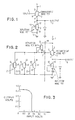
- FIG. 1 a circuit diagram is provided that illustrates the improved driving stage of the invention.
- an enhancement mode type field effect transistor 2 is connected with one ohmic electrode 3, such as the source electrode connected to terminal 1, and the other ohmic electrode 4, such as the drain electrode connected to a node 5 to which the output 6 is connected.
- a logic input signal is applied at terminal 7 which is connected to the gate 8 of the enhancement mode field effect transistor 2.
- a depletion mode type field effect transistor 9 having one ohmic electrode 10 thereof, such as the source electrode is connected to ground 11.
- the other ohmic electrode 12 such as the drain electrode is connected to the node 5.
- the gate 13 of transistor 9 is connected to ground 11.
- the driving stage of the invention shown in FIG. 1 has features that differ from the conventional source/follower type digital logic signal amplification stage circuitry used heretofore in the art.
- One feature is that the logic input signal is introduced into the circuit through an enhancement mode type field effect transistor.
- the enhancement mode type field effect transistor has the characteristic that in the absence of a signal above the threshold is in the "off" condition. In the “off” condition, the enhancement mode type transistor 2 exhibits a high impedance which establishes the lower signal level of the circuit at the output 6 at a very precise value. In the “on” condition, the enhancement mode type transistor 2 exhibits a low impedance which establishes the higher signal level of the circuit at the output 6.
- the depletion mode type field effect transistor 9 has the source 10 electrode thereof connected to the gate 13 and directly to ground 11. This performs two functions. The first is that the signal level at the output 6 is firmly established at ground. The second is in signal shaping in that when the logic input signal at 7 causes the enhancement mode type field effect transistor 2 to turn "off", the depletion mode type field effect transistor 9 with the source 10 and the gate 13 connected to ground 12 draws off all current and thereby compensates for any circuit reactance in subsequent circuitry connected to the output 6.
- the driving stage of the invention achieves the advantages with the absolute minimum of components and voltages thereby improving yield in fabrication, higher density and the performance advantages of establishing a clear lower digital output signal level, compensation for subsequent circuit reactance properties, and the establishment of a clear maximum upper digital output signal level.
- the driving stage output circuits of the type of the invention are usually connected in practice as an input to a subsequent logic stage circuit and the forward characteristic of a diode is employed to establish greater precision in the higher digital output signal.
- the subsequent logic circuit employs the gate of an FET transistor as in input location the gate to source or drain electrode is employed as such a diode.
- the diode is shown dotted in FIG. 1 between the output 6 and ground 11.
- the driving stage illustrated in connection with FIG. 1 when combined with digital logic circuitry employing enhancement mode type field effect transistors as digital logic variable input devices and employing a depletion mode transistor connected as a non-linear load provides a principle for a family of digital logical circuit units where switching in each stage is performed with an enhancement mode transistor and the load is performed with a depletion mode transistor providing both "on" and "off" signal level and shaping precision.
- the combined logic and driving stage units will be illustrated employing a three input variable negative output signal logic circuit, known in the art as a "NOR", although in the light of the principles set forth, it will be apparent that various combinations of parallel and series variable inputs providing "and” and “or”, and combinations thereof, logic functions through enhancement mode type field effect switches, can be assembled.
- NOR three input variable negative output signal logic circuit
- FIG. 2 an illustration is provided of the cooperation between an enhance deplete mode type digital logic circuitry and the driving stage of FIG. 1 as a unit.
- FIG. 2 an imaginary line 14 shown dotted, separates the logic stage and the driving stage of the circuit.
- the same numerals as in FIG. 1 are used.
- the logic circuit there is provision for three independent digital logic variables A, B and C.
- the signal representing each logic variable in the "on” condition is greater than the threshold of the enhancement mode transistor to which it is applied.
- the corresponding transistor turns “on” causing the signal level at the node 7 to move in the direction of ground.
- three enhancement mode type field effect transistors 15, 16 and 17 are provided with gates 18, 19 and 20 for logic variables A, B and C, respectively, which in turn are to be applied to terminals 21, 22 and 23.
- the three enhancement mode type transistors 15, 16 and 17 each have their source electrodes 24, 25 and 26, respectively, connected to the ground at 12, and each have their drain electrodes 27, 28 and 29, respectively, connected to the node 7 which is the output of the logic portion and the input of the driving portion of the circuit.
- the level at the node 7 is established by the non-linear load which function is performed by the depletion mode type field effect transistor 30, having the drain electrode 31 thereof connected to the node 7, having the source electrode 32 thereof connected to the voltage 1 and having the gate 33 thereof connected to the node 7.
- the driving stage output 6 will be connected to the gate of a logic variable input of a subsequent stage, such as a gate of a transistor 15, 16 or 17 and the forward characteristic of the gate to source diode of the transistor establishes a precise higher digital signal level. That diode is schematically shown dotted between the output 6 and ground 11.
- the transistors 15, 16 and 17 being enhancement mode type field effect transistors, in the absence of a positive signal exceeding the threshold at A, B or C are in the "off" or non-conducting condition. Since the three transistors 15, 16 and 17 provide, under these conditions, a high impedance, the voltage level at the node 7 is essentially at the power supply voltage level at terminal 1 since the depletion mode type transistor 30 is conducting. The power supply level at node 7 causes the enhancement mode transistor 2 to turn on raising the signal level at the output 6 to the upper digital level established by the forward characteristic of the gate to source diode, shown dotted, of the next circuit unit.
- the transistor 9 serves as a current sink draining off any current resulting from reactance in subsequent logic circuit unit circuitry connected to the node 6 and permitting an abrupt drop to ground establishing the lower digital output level at the node 6.
- the circuit of FIG. 2 would be provided on a semi-insulating GaAs substrate.
- the depletion and enhancement mode devices would be formed by selective doping using such techniques as ion implantation.
- the voltage would be 1.5 volts.
- the enhancement mode devices would have a threshold of +0.05 volts.
- the depletion mode devices would have a threshold of -0.65 volts.
- the gates may be formed by metal deposition over oxide.
- a curve of the output characteristic at node 6 illustrates the response in relation to an input at A, B or C.
- the potential at the output 6 would drop from 0.83 volts to essentially ground with the application of an input variable signal of the order of 0.83 volts.
Landscapes
- Engineering & Computer Science (AREA)
- Physics & Mathematics (AREA)
- Computer Hardware Design (AREA)
- Computing Systems (AREA)
- General Engineering & Computer Science (AREA)
- Mathematical Physics (AREA)
- Power Engineering (AREA)
- Logic Circuits (AREA)
Applications Claiming Priority (2)
| Application Number | Priority Date | Filing Date | Title |
|---|---|---|---|
| US856630 | 1986-04-25 | ||
| US06/856,630 US4725743A (en) | 1986-04-25 | 1986-04-25 | Two-stage digital logic circuits including an input switching stage and an output driving stage incorporating gallium arsenide FET devices |
Publications (2)
| Publication Number | Publication Date |
|---|---|
| EP0242523A2 true EP0242523A2 (de) | 1987-10-28 |
| EP0242523A3 EP0242523A3 (de) | 1989-02-08 |
Family
ID=25324122
Family Applications (1)
| Application Number | Title | Priority Date | Filing Date |
|---|---|---|---|
| EP87102195A Ceased EP0242523A3 (de) | 1986-04-25 | 1987-02-17 | Integrierte Steuerungsstufe für logische FET-Schaltung |
Country Status (4)
| Country | Link |
|---|---|
| US (1) | US4725743A (de) |
| EP (1) | EP0242523A3 (de) |
| JP (1) | JPS62256531A (de) |
| CA (1) | CA1265590A (de) |
Families Citing this family (9)
| Publication number | Priority date | Publication date | Assignee | Title |
|---|---|---|---|---|
| US4965863A (en) * | 1987-10-02 | 1990-10-23 | Cray Computer Corporation | Gallium arsenide depletion made MESFIT logic cell |
| US4806785A (en) * | 1988-02-17 | 1989-02-21 | International Business Machines Corporation | Half current switch with feedback |
| JPH01300714A (ja) * | 1988-05-30 | 1989-12-05 | Norio Akamatsu | 負荷電流制御型論理回路 |
| US4885480A (en) * | 1988-08-23 | 1989-12-05 | American Telephone And Telegraph Company, At&T Bell Laboratories | Source follower field-effect logic gate (SFFL) suitable for III-V technologies |
| US4931670A (en) * | 1988-12-14 | 1990-06-05 | American Telephone And Telegraph Company | TTL and CMOS logic compatible GAAS logic family |
| US4954730A (en) * | 1989-04-21 | 1990-09-04 | The Board Of Trustees Of The Leland Stanford Junior University | Complementary FET circuit having merged enhancement/depletion FET output |
| US5182473A (en) * | 1990-07-31 | 1993-01-26 | Cray Research, Inc. | Emitter emitter logic (EEL) and emitter collector dotted logic (ECDL) families |
| US5045723A (en) * | 1990-07-31 | 1991-09-03 | International Business Machines Corporation | Multiple input CMOS logic circuits |
| US5187394A (en) * | 1992-01-13 | 1993-02-16 | Motorola, Inc. | Configurable row decoder driver circuit |
Family Cites Families (21)
| Publication number | Priority date | Publication date | Assignee | Title |
|---|---|---|---|---|
| US3299291A (en) * | 1964-02-18 | 1967-01-17 | Motorola Inc | Logic elements using field-effect transistors in source follower configuration |
| US3678293A (en) * | 1971-01-08 | 1972-07-18 | Gen Instrument Corp | Self-biasing inverter |
| FR2264434B1 (de) * | 1974-03-12 | 1976-07-16 | Thomson Csf | |
| JPS5342587B2 (de) * | 1974-04-23 | 1978-11-13 | ||
| US4038563A (en) * | 1975-10-03 | 1977-07-26 | Mcdonnell Douglas Corporation | Symmetrical input nor/nand gate circuit |
| US4177390A (en) * | 1977-12-27 | 1979-12-04 | Raytheon Company | A field effect transistor logic gate having depletion mode and enhancement mode transistors |
| JPS54158848A (en) * | 1978-06-06 | 1979-12-15 | Nippon Precision Circuits | Semiconductor circuit device |
| FR2449369A1 (fr) * | 1979-02-13 | 1980-09-12 | Thomson Csf | Circuit logique comportant une resistance saturable |
| FR2478907A1 (fr) * | 1980-03-21 | 1981-09-25 | Thomson Csf | Inverseur utilisant des transistors a effet de champ a faible tension de seuil et une diode de commutation, realise en circuit integre, et circuit logique comportant un tel inverseur |
| FR2483146A1 (fr) * | 1980-05-23 | 1981-11-27 | Thomson Csf | Operateur logique rapide, a grande entrance, a fonction logique complexe, utilisant au moins un transistor a effet de champ a faible tension de seuil |
| FR2485832A1 (fr) * | 1980-06-24 | 1981-12-31 | Thomson Csf | Inverseur logique, et operateur a plusieurs sorties derive de cet inverseur, utilisant au moins un transistor a effet de champ a faible tension de seuil |
| DE3177270D1 (de) * | 1980-10-15 | 1992-02-27 | Toshiba Kawasaki Kk | Halbleiterspeicher mit datenprogrammierzeit. |
| US4395645A (en) * | 1980-12-05 | 1983-07-26 | International Telephone And Telegraph Corporation | Mosfet logic inverter buffer circuit for integrated circuits |
| US4405870A (en) * | 1980-12-10 | 1983-09-20 | Rockwell International Corporation | Schottky diode-diode field effect transistor logic |
| US4423339A (en) * | 1981-02-23 | 1983-12-27 | Motorola, Inc. | Majority logic gate |
| JPS56138335A (en) * | 1981-03-09 | 1981-10-28 | Hitachi Ltd | Integrated circuit |
| US4438351A (en) * | 1981-06-09 | 1984-03-20 | Schuermeyer Fritz L | Gallium arsenide MIS integrated circuits |
| US4445051A (en) * | 1981-06-26 | 1984-04-24 | Burroughs Corporation | Field effect current mode logic gate |
| US4490632A (en) * | 1981-11-23 | 1984-12-25 | Texas Instruments Incorporated | Noninverting amplifier circuit for one propagation delay complex logic gates |
| US4404480A (en) * | 1982-02-01 | 1983-09-13 | Sperry Corporation | High speed-low power gallium arsenide basic logic circuit |
| JPS58145237A (ja) * | 1982-02-22 | 1983-08-30 | Matsushita Electric Ind Co Ltd | 電界効果トランジスタの論理回路 |
-
1986
- 1986-04-25 US US06/856,630 patent/US4725743A/en not_active Expired - Fee Related
-
1987
- 1987-02-17 EP EP87102195A patent/EP0242523A3/de not_active Ceased
- 1987-03-05 JP JP62049019A patent/JPS62256531A/ja active Pending
- 1987-03-11 CA CA000531779A patent/CA1265590A/en not_active Expired
Also Published As
| Publication number | Publication date |
|---|---|
| JPS62256531A (ja) | 1987-11-09 |
| CA1265590A (en) | 1990-02-06 |
| US4725743A (en) | 1988-02-16 |
| EP0242523A3 (de) | 1989-02-08 |
Similar Documents
| Publication | Publication Date | Title |
|---|---|---|
| EP0100213B1 (de) | VLSI-Chip aus Galliumarsenid | |
| KR930000968B1 (ko) | 반도체 집적회로 | |
| US6130570A (en) | MESFET circuit utilizing only positive power supplies | |
| EP0243603A2 (de) | Binäre logische Schaltung | |
| EP0075915B1 (de) | Logische Schaltung gespeist durch nur eine Spannung | |
| EP0053664B1 (de) | Integriertes logisches Tor | |
| EP0337078A2 (de) | Logische Schaltung hoher Geschwindigkeit | |
| JPS6447125A (en) | Multi-input logic gate | |
| EP0263006A1 (de) | Schaltungsanordnung für einen Differenzverstärker | |
| US4725743A (en) | Two-stage digital logic circuits including an input switching stage and an output driving stage incorporating gallium arsenide FET devices | |
| US3573490A (en) | Capacitor pull-up reigister bit | |
| US4698524A (en) | MESFET logic using integral diode level shifting | |
| GB2327544A (en) | Monolithic MOS analogue switch with increased signal voltage range | |
| US4092548A (en) | Substrate bias modulation to improve mosfet circuit performance | |
| EP0316033A1 (de) | Integrierte Digitalschaltung | |
| EP0200230A2 (de) | Auf einem Verbundhalbleitersubstrat gebildete logische integrierte Schaltungsvorrichtung | |
| EP0562719B1 (de) | Integriertes Schaltkreisbauelement, gebildet aus einem Verbindungshalbleiter | |
| US4639621A (en) | Gallium arsenide gate array integrated circuit including DCFL NAND gate | |
| US4857984A (en) | Three-terminal MOS integrated circuit switch | |
| US4712022A (en) | Multiple input OR-AND circuit for FET logic | |
| EP0282249B1 (de) | Logische Schaltung mit Feldeffekttransistor, der eine Verbindung mit gleichrichtender Charakteristik zwischen Gatter und Quelle aufweist | |
| EP0170134B1 (de) | Schottky-Dioden und Feldeffekt-Transistoren verwendende Logikschaltung | |
| KR890004770B1 (ko) | 논리 회로 | |
| US5291077A (en) | Semiconductor logical FET device | |
| JPH02182029A (ja) | 半導体装置 |
Legal Events
| Date | Code | Title | Description |
|---|---|---|---|
| PUAI | Public reference made under article 153(3) epc to a published international application that has entered the european phase |
Free format text: ORIGINAL CODE: 0009012 |
|
| AK | Designated contracting states |
Kind code of ref document: A2 Designated state(s): DE FR GB IT |
|
| 17P | Request for examination filed |
Effective date: 19880224 |
|
| PUAL | Search report despatched |
Free format text: ORIGINAL CODE: 0009013 |
|
| AK | Designated contracting states |
Kind code of ref document: A3 Designated state(s): DE FR GB IT |
|
| 17Q | First examination report despatched |
Effective date: 19900111 |
|
| STAA | Information on the status of an ep patent application or granted ep patent |
Free format text: STATUS: THE APPLICATION HAS BEEN REFUSED |
|
| 18R | Application refused |
Effective date: 19911129 |
|
| RIN1 | Information on inventor provided before grant (corrected) |
Inventor name: ANDERSON, CARL JOHN |