EP0200230B1 - Auf einem Verbundhalbleitersubstrat gebildete logische integrierte Schaltungsvorrichtung - Google Patents
Auf einem Verbundhalbleitersubstrat gebildete logische integrierte Schaltungsvorrichtung Download PDFInfo
- Publication number
- EP0200230B1 EP0200230B1 EP86106035A EP86106035A EP0200230B1 EP 0200230 B1 EP0200230 B1 EP 0200230B1 EP 86106035 A EP86106035 A EP 86106035A EP 86106035 A EP86106035 A EP 86106035A EP 0200230 B1 EP0200230 B1 EP 0200230B1
- Authority
- EP
- European Patent Office
- Prior art keywords
- transistors
- output
- transistor
- terminal
- compound semiconductor
- Prior art date
- Legal status (The legal status is an assumption and is not a legal conclusion. Google has not performed a legal analysis and makes no representation as to the accuracy of the status listed.)
- Expired - Lifetime
Links
- 239000000758 substrate Substances 0.000 title claims description 17
- 239000004065 semiconductor Substances 0.000 title claims description 15
- 150000001875 compounds Chemical class 0.000 title claims description 9
- JBRZTFJDHDCESZ-UHFFFAOYSA-N AsGa Chemical compound [As]#[Ga] JBRZTFJDHDCESZ-UHFFFAOYSA-N 0.000 claims description 28
- 229910001218 Gallium arsenide Inorganic materials 0.000 claims description 28
- XUIMIQQOPSSXEZ-UHFFFAOYSA-N Silicon Chemical compound [Si] XUIMIQQOPSSXEZ-UHFFFAOYSA-N 0.000 claims description 5
- 229910052710 silicon Inorganic materials 0.000 claims description 5
- 239000010703 silicon Substances 0.000 claims description 5
- 230000004044 response Effects 0.000 claims description 4
- VYPSYNLAJGMNEJ-UHFFFAOYSA-N Silicium dioxide Chemical compound O=[Si]=O VYPSYNLAJGMNEJ-UHFFFAOYSA-N 0.000 description 6
- 239000008186 active pharmaceutical agent Substances 0.000 description 5
- 150000002500 ions Chemical class 0.000 description 5
- 230000003247 decreasing effect Effects 0.000 description 3
- 230000005669 field effect Effects 0.000 description 3
- 229920002120 photoresistant polymer Polymers 0.000 description 3
- 235000012239 silicon dioxide Nutrition 0.000 description 3
- 239000000377 silicon dioxide Substances 0.000 description 3
- 230000000295 complement effect Effects 0.000 description 2
- 238000010586 diagram Methods 0.000 description 2
- 230000000694 effects Effects 0.000 description 2
- 238000005468 ion implantation Methods 0.000 description 2
- 238000004519 manufacturing process Methods 0.000 description 2
- 230000008018 melting Effects 0.000 description 2
- 238000002844 melting Methods 0.000 description 2
- 229910052751 metal Inorganic materials 0.000 description 2
- 239000002184 metal Substances 0.000 description 2
- 238000000034 method Methods 0.000 description 2
- 239000003990 capacitor Substances 0.000 description 1
- 230000008859 change Effects 0.000 description 1
- 238000005229 chemical vapour deposition Methods 0.000 description 1
- 238000010276 construction Methods 0.000 description 1
- 238000001312 dry etching Methods 0.000 description 1
- 238000012986 modification Methods 0.000 description 1
- 230000004048 modification Effects 0.000 description 1
- 230000009467 reduction Effects 0.000 description 1
- 230000000630 rising effect Effects 0.000 description 1
- 229920006395 saturated elastomer Polymers 0.000 description 1
- 238000004544 sputter deposition Methods 0.000 description 1
- WQJQOUPTWCFRMM-UHFFFAOYSA-N tungsten disilicide Chemical compound [Si]#[W]#[Si] WQJQOUPTWCFRMM-UHFFFAOYSA-N 0.000 description 1
- 229910021342 tungsten silicide Inorganic materials 0.000 description 1
Images


Classifications
-
- H—ELECTRICITY
- H03—ELECTRONIC CIRCUITRY
- H03K—PULSE TECHNIQUE
- H03K19/00—Logic circuits, i.e. having at least two inputs acting on one output; Inverting circuits
- H03K19/0175—Coupling arrangements; Interface arrangements
- H03K19/0185—Coupling arrangements; Interface arrangements using field effect transistors only
- H03K19/018507—Interface arrangements
- H03K19/018535—Interface arrangements of Schottky barrier type [MESFET]
- H03K19/018542—Interface arrangements of Schottky barrier type [MESFET] with at least one differential stage
-
- H—ELECTRICITY
- H03—ELECTRONIC CIRCUITRY
- H03K—PULSE TECHNIQUE
- H03K19/00—Logic circuits, i.e. having at least two inputs acting on one output; Inverting circuits
- H03K19/02—Logic circuits, i.e. having at least two inputs acting on one output; Inverting circuits using specified components
- H03K19/08—Logic circuits, i.e. having at least two inputs acting on one output; Inverting circuits using specified components using semiconductor devices
- H03K19/094—Logic circuits, i.e. having at least two inputs acting on one output; Inverting circuits using specified components using semiconductor devices using field-effect transistors
- H03K19/09432—Logic circuits, i.e. having at least two inputs acting on one output; Inverting circuits using specified components using semiconductor devices using field-effect transistors with coupled sources or source coupled logic
- H03K19/09436—Source coupled field-effect logic [SCFL]
Definitions
- the present invention relates to a logic integrated circuit device formed on a compound semiconductor substrate and more particularly, to such a device which is compatible with a silicon emitter-coupled logic integrated circuit device.
- GaAs IC gallium arsenide
- the inventor developed a prototype GaAs IC, but which satisfied the above three conditions at the sacrifice of a power consumption and a semiconductor chip area. More specifically, some of transistors in the prototype GaAs IC were connected in series between power supply terminals. The power supply voltage applied to the IC was -5,2 V , so that each of the series-connected transistors was supplied with a small voltage across its source and drain. Therefore, the threshold voltage thereof had to be designed to be of a shallow value. All the transistors in the prototype GaAs IC were fabricated through the same steps, and thus took the same threshold voltage. As a result, the threshold voltage of an output transistor became shallow inevitably. On the other hand, the output transistor should drive to 50 ⁇ load and produce an output signal having the ECL level.
- the output transistor is required to have a considerably large current ability.
- its gate width was made large remarkably.
- the area on a semiconductor chip occupied by the output transistor was made large.
- the transistor having a large gate width increases its input stray capacitance. For this reason, a plurality of buffer amplifiers were required to drive the output transistor. As a result, a large power was consumed by the buffer amplifiers.
- the amplifiers also increase the chip area.
- US 4 028 556 discloses an integrated logic circuit in which the current drivability of the output stage is larger than that of the input stage.
- one of the transistors constituting the logic circuit has a threshold voltage larger in absolutely value than that of each of the transistors constituting the remaining part of the logic circuit. Therefore, the stray capacitance at the connecting node becomes large so that the operation speed is lowered and large power is consumed. Furthermore, the produced logic levels are not compatible with those of Si-ECLIC.
- a GaAs integrated circuit in which a large current drivability of a source follower stage is achieved.
- the source follower stage is a part of a logic circuit and, therefore, the operation speed is lowered and large power is consumed.
- EP-A-0 085 569 An integrated circuit device according to the preamble part of the claim is described in EP-A-0 085 569.
- the output stage is composed of two elements, a transistor and a diode, in order to achieve the desired output levels.
- the output transistor is required to supply the load with relatively large currents, so that it has to be fabricated with large occupying area and enlarges the stray capacitance thereof so that the operation speed is thereby lowered.
- an integrated circuit device comprising a gallium arsenide substrate, a first power terminal supplied with a ground voltage, a second power terminal supplied with a first negative voltage substantially equal to -5.2 V, a compound semiconductor substrate, a plurality of transistors formed on said compound semiconductor substrate, said plurality of transistors constituting a logic circuit connected between said first and second power terminals, an ECL- compatible output terminal, and an output transistor formed on said compound semiconductor substrate, connected between said first power terminal and said output terminal and having a first threshold voltage, said output terminal being connected through an externally provided load of 50 ohms to a potential source terminal, wherein all of said plurality of transistors have a second threshold voltage within a range from -0.2V to - 0.3V and wherein said first threshold voltage is within a range from -0.6V to -0.9V, said potential source terminal is supplied with a second negative voltage, the source of said output transistor is connected directly to the output terminal, and wherein said output transistor is turned OFF in response to a first state
- the output transistor has a deeper threshold voltage and hence a large current value with a considerably small gate width. Therefore, the chip area occupied by the output transistor is made small.
- the input stray capacitance of the output transistor is also decreased, and accordingly only one or no buffer amplifier is required to drive the output transistor. The power consumption is thereby reduced and the chip area is further decreased.
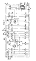
- a GaAs IC 100 has four input terminals 1 to 4, two output terminals 7 and 8, and two power supply terminals 5 and 6.
- the first input terminal 1 is connected to the gate of a transistor Q9 via a first input circuit which is composed of a source follower transistor Q1, a current source transistor Q2, two level shift diodes D1 and D2, and two bias resistors R1 and R2.
- the second input terminal 2 is connected to the gate of a transistor Q12 through a second input circuit composed of a source follower transistor Q3, a current source transistor Q4, a level shift diode D3, and bias resistors R3 and R4.
- the third input terminal 2 is connected via a third input circuit to the gate of a transistor Q15.
- the third input circuit is constituted of a source follower transistor Q5, a current source transistor Q6, level shift diodes D4 and D5, and bias resistors R5 and R6.
- the fourth input terminal 4 is connected to the gate of a transistor Q10 via a fourth input circuit which is composed of a source follower transistor Q7, a current source transistor Q8, a level shift diode D6, and bias resistors R7 and R8.
- the transistors Q9 and Q10 constitutes a differential circuit, and the source connection point thereof is connected to a current source transistor Q11.
- the transistors Q12 and Q15 also constitutes a differential cirucit, and a transistor Q9 operates as a current source thereof.
- a transistor Q11 operates as a current source of a differential circuit composed of the transistors Q13 and Q14.
- the drains of the transistors Q12 and Q13 are connected in common to one ends of a load resistor R10 and further to the gate of a transistor Q16.
- the drains of the transistors Q14 and Q15 are connected in common to one end of a load resistor R11 and to the gate of a source follower transistor Q18.
- the other ends of the load resistors R10 and R11 are connected via a level adjusting resistor R9 to the first power supply terminal 5.
- the source outputs of the transistors Q16 and Q18 are fed back through diodes D7 and D8 to the gates of the transistors Q14 and Q13, respectively.
- Transistors Q17 and Q19 constitutes a current source.
- the transistors Q9 to Q15 and the resistors R9 to R11 thus constitutes a differential type logic circuit which functions as a latch circuit.
- the outputs of the source follower transistors Q16 and Q13 are supplied through the diodes D7 and D8 to a first buffer amplifier which is composed of transistors Q20 to Q26, resistors R12 to R14 and diodes D9 and D10.
- a first buffer amplifier which is composed of transistors Q20 to Q26, resistors R12 to R14 and diodes D9 and D10.
- the transistors Q20 and Q21 are connected in a differential form, and the transistor Q22 is a current source.
- the resistors R13 and R14 are load resistors and R12 is a level adjusting resistor.
- the transistors Q23 to Q26 and the diodes D9 and D10 constitute a level shift circuit.
- the outputs of the first buffer amplifier are supplied to a second buffer amplifier 9.
- the second buffer amplifier 9 has the same construction as the first amplifier and therefore is respresented as a block circuit.
- the outputs of the second buffer amplifier 9 are supplied respectively to source follower transistors Q27 and Q28 which have their sources connected respectively to the output terminals 7 and 8 and operate as output transistors.
- the output terminals 7 and 8 are connected respectively to an external power terminal 10 and further to a subsequent stage circuit (not shown).
- Each of the transistors Q1 to Q28 is of an N-channel type and a Schottky junction type field effect transistor.
- the inventor developed the prototype GaAs IC 100, so that he clarified that the IC 100 sacrificed the power consumption and the chip area for the compatibility with an Si-ECL IC and for a high speed operation.
- the latch circuit including the transistors Q9 to Q15 and the buffer amplifiers employed a differential type logic circuit to produce true and complementary signals.
- condition (2) for the compatibility was thus satisfied.
- the first power supply terminal 5 was grounded and the second power supply terminal 6 was applied with a V SS potential of -5.2 V .
- the input terminals 1 and 4 and thoses 2 and 3 where used respectively as a pair of input terminals. Accordingly, one of the terminals 1 and 4 and one of those 2 and 3 were often in an open state.
- Each of input signals IN1 to IN4 took on ECL level in which a high level and a low level were -0.7 V and -1,9 V , respectively.
- the resistance values of the resistors R1, R3, R5 and R7 were 1,3K ⁇ , and those of the resistors R2, R4, R6 and R8 were 4.9K ⁇ , so that the gate biases of the transistors Q1, Q3, Q5 and Q7 were designed to be an intermediate level of the high level and the low level of the input signal IN. As a result, the compatibility was also satisfied with respect to the input signal logic level.
- V DS > V DS(SAT) V GS - V T (1)
- V DS is a voltage between source and drain
- V DS(SAT) is a drain-source voltage at a saturation point
- V GS is a gate-source voltage
- V T is a threshold voltage.
- the conductance of the transistor is increased by a large V GS , so that the transistor operates at a high speed.
- V GS exceeds 0.6 V
- the Schottky gate is forward biased, so that a gate current flows. Therefore, V GS is designed to be within a range between 0.4 V and 0.6 V .
- V DSA voltage drop across the level adjusting resistor R9
- V LS voltage drop across the resistor R10 (or R11)
- the voltage drop V LS across the resistor R10 (or R11) was an amplitude of signals supplied to the transistors Q14 (or Q13) and Q20 (ord Q21) and tooks 2 V to obtain a switching operation in these transistors.
- the voltage drop V R9 across the resistor R9 required 0.6 V in order that the transistors Q12 and Q13 and those Q14 and Q15 operated in a differential form.
- the voltage V DSA was under 2.6 V from the equation (2).
- the respective drain-source voltages of the series- connected three transistors were thereby about 0.8 V .
- the gate-source voltage V GS of 0.4 to 0.6 V was supplied to each of those three transistors.
- the threshold voltage V T of the respective transistors took -0.2 to -0.3 V from the relationship (1) and could not be designed to be more deeply than this value. All the transistors in the IC 100 were manufactured by the same steps, and therefore the remaining transistors Q1 to Q8 and Q16 to Q28 also took their threshold voltage of -0.2 to -0.3 V .
- Fig. 3 shows the relationship of the drain current I DS to the gate width. Since the threshold voltages V T of the transistors Q27 and Q28 were -0.2 V , that relationship is represented by a line 200. The gate width of 450 ⁇ m was recessitated for the current ability of 20 mA.
- the GaAs IC 100 required the considerably large sized output transistors Q27 and Q28, so that the area of a semiconductor chip was enlarged. Since the gate widths of the transistors Q27 and Q28 were large, their input stray capacitors were made large remarkably. For this reason, it was impossible that the transistors Q27 and Q28 are driven only by the transistors Q23 and Q25 at a high speed. Therefore, the second buffer amplifier 9 was inserted between the first amplifier and the output transistors. Buffer amplifiers more than two were often provided. The respective transistors in the buffer amplifier 9 were required to have a relatively large gate width in order to drive a considerably large load capacitance, so that the power consumption of the amplifier was increased. The chip area was further enlarged. As described above, the GaAs IC 100 having the compatibility with the Si-ECL IC consumed a large power and required a large chip area.
- Fig. 2 shows an equivalent circuit of a GaAs IC 500 according to an embodiment of the present invention.
- output transistors are represented by Q30 and Q31 and have their threshold voltage that is smaller (or larger in absolute value) than the output transistors Q27 and Q28 in Fig. 1. Since the transistors Q30 and Q31 have a small threshold voltage, and they produce the same drain currents as the transistor Q27 and Q28 with smaller gate width. The transistors Q30 and Q31 are thereby manufactured with a small size to reduce the chip area. The input stray capacitances of Q30 and Q31 are also made small.
- the transistors Q30 and Q31 are driven by the first buffer amplifier composed of the transistors Q20 to Q26, the diodes D9 and D10 and the resistors R12 to R14.
- the second buffer amplifier 9 is thereby unnecessitated.
- the first to fourth input circuit for the first to fourth input signals IN1 to IN4 and the differential type logic circuit as a latch circuit are the same as those in Fig. 1.
- the like reference characters are employed. Accordingly, for the compatibility with the Si-ECL IC and the high speed operation, the threshold voltages of the transistors Q1 to Q28 are -0.2 to -0.3 V , and the resistance values of the resistors R1, R3, R5 and R7 are 1.3K ⁇ , the values of the resistors R2, R4, R6 and R8 being 4.9K ⁇ .
- the first power supply terminal 5 is grounded and the terminal 6 is applied with -5.2 V .
- the transistors Q1 to Q26, Q30 and Q31 are N-channel type Schottky junction field effect transistors.
- the threshold voltages of the output transistors Q30 and Q31 are designed to be -0.65 V . Therefore, the characteristic of the drain current to the gate width in the transistors Q30 and Q31 is represented by a line 300 in Fig. 3.
- the transistors Q30 and Q31 have their current ability of 20 mA with their gate widths of 170 ⁇ m. As a result, the sizes of the transistors Q30 and Q31 is reduced to about one third of the transistors Q27 and Q28.
- the input stray capacitance of a transistor also depends on its threshold voltage. However, the increase in the input stray capacitance caused by the increase in threshold voltage is suppressed below 20 % in this embodiment. As a result, the second buffer amplifier 9 shown in Fig. 1 is deleted. This result in the further decrease in the chip area and a remarkable reduction of a power consumption.
- the semiconductor chip area of the GaAs IC 500 is reduced by 30 to 40 % as compared to that of the GaAs IC 100. The power consumption is also decreased similarly.
- the present invention provides a GaAs IC having compatibility with an Si-ECL IC without increasing a power consumption and a chip area.
- the threshold voltages of the output transistors Q30 and Q31 are favourably designed to be within a range between -0.6 V and -0.9 V .
- Fig. 4 to Fig. 8 show manufacturing steps of the output transistor Q30 (Q31) and the logic section transistor Q9 (Q1 to Q8 and Q10 to Q26).
- a semi-insulating gallium arsenide substrate 50 is prepared, and a main surface thereof is covered selectively with a photoresist film 51.
- Si+ ions are implanted into an exposed portion of the substrate 50 by ion implantation technique to form a channel region 52 of the output transistor Q30 (Q31).
- the photoresist film 51 is then removed, and a new photo-resist film 53 is formed to cover selectively the surface of the substrate 50, as shown in fig. 5.
- Si+ ions are implanted to the selective portion of the substrate 50 to form a channel region 54 of the transistor Q9 (Q1 to Q8 and Q10 to Q26).
- the ion energy is 40 Kev
- the dose amount is 5 to 6 x 1012 cm ⁇ 2.
- the ion energy and the dose amount for the channel region 54 are 40 KeV and 4 x 1012 cm ⁇ 3, respectively.
- the channel region 52 presents -0.6 to -0.9 V threshold voltage to the output transistors Q30 and Q31
- the channel region 54 presents a threshold voltage below -0.3 V to the transistor Q1 to Q26.
- the photoresist film 53 is removed, and a high melting point metal such as a tungsten silicide is deposited over the surface of the substrate 50 by the sputtering method.
- the high melting point metal is subjected to the selective dry etching, so that Schottky gate electrode 55 and 56 are formed as shown in Fig. 6.
- the gate width of the gate 55 is designed to present the above-mentioned current ability.
- an insulating film 57 such as silicon dioxide is deposited over the gate electrodes 55 and 56 and the surface of the substrate 50.
- the film 57 is selectively removed, so that only on the side surfaces of the gate electrodes 55 and 56 the silicon dioxide 57 is left, as shown in Fig. 7.
- high carrier concentration layers 58 to 61 operating as source and drain regions are formed on the channel layers 52 and 54 by the chemical vapor deposition method.
- the side surface insulating films 57 separates the gate electrodes 55 and 56 from the layers 58 to 61. Since the high carrier concentration layers 58 to 61 is formed on the surfaces of the channel regions 52 and 54, the so-called short channel effect is suppressed remarkably.
- the layers 58 to 61 present a high gm. in this embodiment, the value of gm is above 300 m s /mm.
- Ohmic electrodes 62 to 65 are thereafter formed, which operate as source and drain electrodes and are made of Au/Ge-Ni.
- an insulating film 66 made of silicon dioxide is formed over the entire surface, and contact holes are formed in the film 66. Interconnection wiring layers 67 to 70 are then formed to construct the circuit shown in Fig. 2.
- the dose amount is changed to obtain the output transistors Q30 and Q31 having the deep threshold voltage, and therefore the increase in cost is suppressed in a minimum value. It is possible that the ion energy is changed. That is, the carrier concentration of the channel regions of the output transistors Q30 and Q31 is increased to make the threshold values therof deep.
- the transistors in the GaAS IC may be of a P-channel type, and output transistors of a source-grounded type may be employed.
Landscapes
- Engineering & Computer Science (AREA)
- Computer Hardware Design (AREA)
- Physics & Mathematics (AREA)
- Computing Systems (AREA)
- General Engineering & Computer Science (AREA)
- Mathematical Physics (AREA)
- Power Engineering (AREA)
- Logic Circuits (AREA)
- Junction Field-Effect Transistors (AREA)
- Amplifiers (AREA)
Claims (1)
- Integrierte Schaltungsvorrichtung mit einem Gallium-Arsenid-Substrat, einer ersten Netzklemme, die mit einer Massespannung gespeist wird, einer zweiten Netzklemme (6), die mit einer ersten negativen Spannung gespeist wird, welche im wesentlichen gleich -5.2V beträgt, einem Verbundhalbleitersubstrat (50), einer Anzahl Transistoren (Q1-Q26), die auf dem Verbundhalbleitersubstrat ausgebildet sind, wobei die Anzahl Transistoren einen logischen Schaltkreis bilden, der zwischen den ersten und zweiten Netzklemmen geschaltet ist, einer ECL-Kompatiblen Ausgangsklemme (7,8), und einem Ausgangstransistor (Q27,Q28), der auf dem Verbundhalbleitersubstrat ausgebildet ist, zwischen der ersten Netzklemme und der Ausgangsklemme geschaltet ist, und eine erste Schwellwertspannung hat, wobei die Ausgangsklemme über eine externe vorgesehene Last von 50 Ω an eine Spannungsquellenklemme (10) angeschlossen ist, dadurch gekennzeichnet, daß alle der Anzahl Transistoren eine zweite Schwellwertspannung innerhalb eines Bereiches von -0.2V bis -0.3V haben, wobei die erste Schwellwertspannung im Bereich von -0.6V bis -0.9V liegt, daß die Spannungsklemme (10) mit einer zweiten negativen Spannung gespeist wird, daß die Source des Ausgangstransistors (Q27,Q28) direkt an die Ausgangsklemme (7,8) angeschlossen ist, und daß der Ausgangstransistor in Abhängigkeit von einem ersten Status eines Ausgangssignals am logischen Schaltkreis AUS-geschaltet und in Abhängigkeit von einem zweiten Status des Ausgangssignals am logischen Schaltkreis EIN-geschaltet wird, um logische Pegel zu erzeugen, die mit denen von Silicium-Emitter-gekoppelten integrierten Logikschaltkreisen kompatibel sind.
Applications Claiming Priority (2)
| Application Number | Priority Date | Filing Date | Title |
|---|---|---|---|
| JP94905/85 | 1985-05-02 | ||
| JP9490585 | 1985-05-02 |
Publications (3)
| Publication Number | Publication Date |
|---|---|
| EP0200230A2 EP0200230A2 (de) | 1986-11-05 |
| EP0200230A3 EP0200230A3 (en) | 1987-04-08 |
| EP0200230B1 true EP0200230B1 (de) | 1991-09-04 |
Family
ID=14123034
Family Applications (1)
| Application Number | Title | Priority Date | Filing Date |
|---|---|---|---|
| EP86106035A Expired - Lifetime EP0200230B1 (de) | 1985-05-02 | 1986-05-02 | Auf einem Verbundhalbleitersubstrat gebildete logische integrierte Schaltungsvorrichtung |
Country Status (4)
| Country | Link |
|---|---|
| US (1) | US4743957A (de) |
| EP (1) | EP0200230B1 (de) |
| JP (1) | JPS62283718A (de) |
| DE (1) | DE3681193D1 (de) |
Families Citing this family (11)
| Publication number | Priority date | Publication date | Assignee | Title |
|---|---|---|---|---|
| FR2594610A1 (fr) * | 1986-02-18 | 1987-08-21 | Labo Electronique Physique | Dispositif semiconducteur du type reseau de portes prediffuse pour circuits a la demande |
| US4831284A (en) * | 1988-03-22 | 1989-05-16 | International Business Machines Corporation | Two level differential current switch MESFET logic |
| FR2648971B1 (fr) * | 1989-06-23 | 1991-09-06 | Thomson Composants Microondes | Circuit d'interface de sortie entre deux circuits numeriques de natures differentes |
| EP0417335A1 (de) * | 1989-09-11 | 1991-03-20 | Siemens Aktiengesellschaft | Schaltungsanordnung zur Wandlung von Signalen mit TTL-Pegel in Signale mit CML-Pegel oder ECL-Pegel |
| DE4006504A1 (de) * | 1990-03-02 | 1991-09-05 | Telefunken Electronic Gmbh | Schaltungsanordnung fuer opto-schmitt-trigger |
| JPH03270319A (ja) * | 1990-03-19 | 1991-12-02 | Fujitsu Ltd | レベル変換回路 |
| JPH0454724A (ja) * | 1990-06-22 | 1992-02-21 | Sumitomo Electric Ind Ltd | 論理回路 |
| JPH07226667A (ja) * | 1993-06-22 | 1995-08-22 | Nec Corp | 入力回路 |
| JPH11145397A (ja) * | 1997-11-11 | 1999-05-28 | Mitsubishi Electric Corp | 半導体集積回路装置 |
| JP2002370363A (ja) * | 2001-06-15 | 2002-12-24 | Canon Inc | インクジェット記録ヘッド用基板、インクジェット記録ヘッド、インクジェット記録装置 |
| CN111404537B (zh) * | 2020-03-05 | 2023-09-26 | 中科亿海微电子科技(苏州)有限公司 | 一种用于fpga的过压输入i/o缓冲器电路 |
Citations (1)
| Publication number | Priority date | Publication date | Assignee | Title |
|---|---|---|---|---|
| EP0085569A2 (de) * | 1982-02-01 | 1983-08-10 | Sperry Corporation | Galliumarsenide logische Schaltung |
Family Cites Families (7)
| Publication number | Priority date | Publication date | Assignee | Title |
|---|---|---|---|---|
| JPS5066146A (de) * | 1973-10-12 | 1975-06-04 | ||
| FR2264434B1 (de) * | 1974-03-12 | 1976-07-16 | Thomson Csf | |
| US4410815A (en) * | 1981-09-24 | 1983-10-18 | Sperry Corporation | Gallium arsenide to emitter coupled logic level converter |
| US4496856A (en) * | 1982-07-21 | 1985-01-29 | Sperry Corporation | GaAs to ECL level converter |
| US4494016A (en) * | 1982-07-26 | 1985-01-15 | Sperry Corporation | High performance MESFET transistor for VLSI implementation |
| JPS59117328A (ja) * | 1982-12-24 | 1984-07-06 | Hitachi Ltd | 論理回路 |
| JPH0773207B2 (ja) * | 1984-05-11 | 1995-08-02 | セイコーエプソン株式会社 | 出力回路 |
-
1986
- 1986-05-02 EP EP86106035A patent/EP0200230B1/de not_active Expired - Lifetime
- 1986-05-02 DE DE8686106035T patent/DE3681193D1/de not_active Expired - Lifetime
- 1986-05-02 US US06/858,984 patent/US4743957A/en not_active Expired - Lifetime
- 1986-05-02 JP JP61102425A patent/JPS62283718A/ja active Pending
Patent Citations (1)
| Publication number | Priority date | Publication date | Assignee | Title |
|---|---|---|---|---|
| EP0085569A2 (de) * | 1982-02-01 | 1983-08-10 | Sperry Corporation | Galliumarsenide logische Schaltung |
Non-Patent Citations (1)
| Title |
|---|
| E. Hölzler, H. Holzwarth "Pulstechnik - Band II, Anwendungen und Systeme", Springer Verlag, Berlin, Heidelberg, New York 1976, pages 155-156 * |
Also Published As
| Publication number | Publication date |
|---|---|
| EP0200230A2 (de) | 1986-11-05 |
| EP0200230A3 (en) | 1987-04-08 |
| US4743957A (en) | 1988-05-10 |
| DE3681193D1 (de) | 1991-10-10 |
| JPS62283718A (ja) | 1987-12-09 |
Similar Documents
| Publication | Publication Date | Title |
|---|---|---|
| US5942940A (en) | Low voltage CMOS differential amplifier | |
| EP0960478B1 (de) | Hochspannungs-cmos-pegelumsetzer | |
| EP0100213B1 (de) | VLSI-Chip aus Galliumarsenid | |
| CA1191972A (en) | High voltage circuits in low voltage cmos process | |
| EP0058958A2 (de) | Komplementäre MOSFET-Logikschaltung | |
| JPS60125015A (ja) | インバ−タ回路 | |
| EP0200230B1 (de) | Auf einem Verbundhalbleitersubstrat gebildete logische integrierte Schaltungsvorrichtung | |
| EP0088291B1 (de) | MOS-Schaltanordnung | |
| EP1251640B1 (de) | Niederspannungskonverter mit Differenzeingang und einem einzigen Ausgang | |
| US4999523A (en) | BICMOS logic gate with higher pull-up voltage | |
| US4864159A (en) | ECL to CMOS transition amplifier | |
| EP0263006A1 (de) | Schaltungsanordnung für einen Differenzverstärker | |
| US5751180A (en) | Electrical device structure having reduced crowbar current and power consumption | |
| US5977800A (en) | Differential MOS current-mode logic circuit having high gain and fast speed | |
| EP0281113B1 (de) | Halbleiter - Pufferschaltung | |
| US4939390A (en) | Current-steering FET logic circuit | |
| US4880998A (en) | Bipolar transistor and CMOS transistor logic circuit having improved discharge capabilities | |
| US4931670A (en) | TTL and CMOS logic compatible GAAS logic family | |
| US6720818B1 (en) | Method and apparatus for maximizing an amplitude of an output signal of a differential multiplexer | |
| HK23694A (en) | Bicmos driver circuit including submicron on-chip voltage source | |
| US5057714A (en) | BiCMOS integrated circuit device utilizing Schottky diodes | |
| US7485931B2 (en) | Semiconductor integrated circuit | |
| JP3152340B2 (ja) | アナログスイッチ回路 | |
| JPH08251007A (ja) | BiCMOS論理ゲート回路 | |
| US5013936A (en) | BiCMOS logic circuit using complementary bipolar transistors having their emitters connected together |
Legal Events
| Date | Code | Title | Description |
|---|---|---|---|
| PUAI | Public reference made under article 153(3) epc to a published international application that has entered the european phase |
Free format text: ORIGINAL CODE: 0009012 |
|
| 17P | Request for examination filed |
Effective date: 19860502 |
|
| AK | Designated contracting states |
Kind code of ref document: A2 Designated state(s): DE FR GB |
|
| PUAL | Search report despatched |
Free format text: ORIGINAL CODE: 0009013 |
|
| AK | Designated contracting states |
Kind code of ref document: A3 Designated state(s): DE FR GB |
|
| 17Q | First examination report despatched |
Effective date: 19890403 |
|
| GRAA | (expected) grant |
Free format text: ORIGINAL CODE: 0009210 |
|
| AK | Designated contracting states |
Kind code of ref document: B1 Designated state(s): DE FR GB |
|
| REF | Corresponds to: |
Ref document number: 3681193 Country of ref document: DE Date of ref document: 19911010 |
|
| ET | Fr: translation filed | ||
| PLBE | No opposition filed within time limit |
Free format text: ORIGINAL CODE: 0009261 |
|
| STAA | Information on the status of an ep patent application or granted ep patent |
Free format text: STATUS: NO OPPOSITION FILED WITHIN TIME LIMIT |
|
| 26N | No opposition filed | ||
| REG | Reference to a national code |
Ref country code: GB Ref legal event code: IF02 |
|
| PGFP | Annual fee paid to national office [announced via postgrant information from national office to epo] |
Ref country code: GB Payment date: 20020501 Year of fee payment: 17 |
|
| PGFP | Annual fee paid to national office [announced via postgrant information from national office to epo] |
Ref country code: FR Payment date: 20020508 Year of fee payment: 17 Ref country code: DE Payment date: 20020508 Year of fee payment: 17 |
|
| PG25 | Lapsed in a contracting state [announced via postgrant information from national office to epo] |
Ref country code: GB Free format text: LAPSE BECAUSE OF NON-PAYMENT OF DUE FEES Effective date: 20030502 |
|
| PG25 | Lapsed in a contracting state [announced via postgrant information from national office to epo] |
Ref country code: DE Free format text: LAPSE BECAUSE OF NON-PAYMENT OF DUE FEES Effective date: 20031202 |
|
| GBPC | Gb: european patent ceased through non-payment of renewal fee |
Effective date: 20030502 |
|
| PG25 | Lapsed in a contracting state [announced via postgrant information from national office to epo] |
Ref country code: FR Free format text: LAPSE BECAUSE OF NON-PAYMENT OF DUE FEES Effective date: 20040130 |
|
| REG | Reference to a national code |
Ref country code: FR Ref legal event code: ST |