EP0099720B1 - Fotovoltaische Vorrichtung - Google Patents
Fotovoltaische Vorrichtung Download PDFInfo
- Publication number
- EP0099720B1 EP0099720B1 EP83304053A EP83304053A EP0099720B1 EP 0099720 B1 EP0099720 B1 EP 0099720B1 EP 83304053 A EP83304053 A EP 83304053A EP 83304053 A EP83304053 A EP 83304053A EP 0099720 B1 EP0099720 B1 EP 0099720B1
- Authority
- EP
- European Patent Office
- Prior art keywords
- layer
- sublayer
- photovoltaic device
- amorphous silicon
- thickness
- Prior art date
- Legal status (The legal status is an assumption and is not a legal conclusion. Google has not performed a legal analysis and makes no representation as to the accuracy of the status listed.)
- Expired
Links
- 229910021417 amorphous silicon Inorganic materials 0.000 claims description 31
- 239000000758 substrate Substances 0.000 claims description 14
- 230000003287 optical effect Effects 0.000 claims description 11
- HBMJWWWQQXIZIP-UHFFFAOYSA-N silicon carbide Chemical compound [Si+]#[C-] HBMJWWWQQXIZIP-UHFFFAOYSA-N 0.000 claims description 3
- AZWHFTKIBIQKCA-UHFFFAOYSA-N [Sn+2]=O.[O-2].[In+3] Chemical compound [Sn+2]=O.[O-2].[In+3] AZWHFTKIBIQKCA-UHFFFAOYSA-N 0.000 claims description 2
- 239000010410 layer Substances 0.000 description 67
- BLRPTPMANUNPDV-UHFFFAOYSA-N Silane Chemical compound [SiH4] BLRPTPMANUNPDV-UHFFFAOYSA-N 0.000 description 9
- 238000009792 diffusion process Methods 0.000 description 6
- 238000010586 diagram Methods 0.000 description 5
- 229910010271 silicon carbide Inorganic materials 0.000 description 4
- 238000006243 chemical reaction Methods 0.000 description 3
- 230000003247 decreasing effect Effects 0.000 description 3
- 230000015572 biosynthetic process Effects 0.000 description 2
- 239000000969 carrier Substances 0.000 description 2
- 238000000354 decomposition reaction Methods 0.000 description 2
- 230000007423 decrease Effects 0.000 description 2
- 230000031700 light absorption Effects 0.000 description 2
- 239000000463 material Substances 0.000 description 2
- 238000000034 method Methods 0.000 description 2
- 239000004065 semiconductor Substances 0.000 description 2
- 239000002356 single layer Substances 0.000 description 2
- 239000004215 Carbon black (E152) Substances 0.000 description 1
- 230000004913 activation Effects 0.000 description 1
- 229910052782 aluminium Inorganic materials 0.000 description 1
- XAGFODPZIPBFFR-UHFFFAOYSA-N aluminium Chemical compound [Al] XAGFODPZIPBFFR-UHFFFAOYSA-N 0.000 description 1
- XPBBUZJBQWWFFJ-UHFFFAOYSA-N fluorosilane Chemical compound [SiH3]F XPBBUZJBQWWFFJ-UHFFFAOYSA-N 0.000 description 1
- 239000008246 gaseous mixture Substances 0.000 description 1
- 239000011521 glass Substances 0.000 description 1
- 229930195733 hydrocarbon Natural products 0.000 description 1
- 150000002430 hydrocarbons Chemical class 0.000 description 1
- 239000012535 impurity Substances 0.000 description 1
- 238000004519 manufacturing process Methods 0.000 description 1
- 238000005215 recombination Methods 0.000 description 1
- 230000006798 recombination Effects 0.000 description 1
- 229910000077 silane Inorganic materials 0.000 description 1
Images

Classifications
-
- H—ELECTRICITY
- H10—SEMICONDUCTOR DEVICES; ELECTRIC SOLID-STATE DEVICES NOT OTHERWISE PROVIDED FOR
- H10F—INORGANIC SEMICONDUCTOR DEVICES SENSITIVE TO INFRARED RADIATION, LIGHT, ELECTROMAGNETIC RADIATION OF SHORTER WAVELENGTH OR CORPUSCULAR RADIATION
- H10F10/00—Individual photovoltaic cells, e.g. solar cells
- H10F10/10—Individual photovoltaic cells, e.g. solar cells having potential barriers
- H10F10/17—Photovoltaic cells having only PIN junction potential barriers
-
- H—ELECTRICITY
- H10—SEMICONDUCTOR DEVICES; ELECTRIC SOLID-STATE DEVICES NOT OTHERWISE PROVIDED FOR
- H10F—INORGANIC SEMICONDUCTOR DEVICES SENSITIVE TO INFRARED RADIATION, LIGHT, ELECTROMAGNETIC RADIATION OF SHORTER WAVELENGTH OR CORPUSCULAR RADIATION
- H10F30/00—Individual radiation-sensitive semiconductor devices in which radiation controls the flow of current through the devices, e.g. photodetectors
- H10F30/20—Individual radiation-sensitive semiconductor devices in which radiation controls the flow of current through the devices, e.g. photodetectors the devices having potential barriers, e.g. phototransistors
- H10F30/21—Individual radiation-sensitive semiconductor devices in which radiation controls the flow of current through the devices, e.g. photodetectors the devices having potential barriers, e.g. phototransistors the devices being sensitive to infrared, visible or ultraviolet radiation
- H10F30/22—Individual radiation-sensitive semiconductor devices in which radiation controls the flow of current through the devices, e.g. photodetectors the devices having potential barriers, e.g. phototransistors the devices being sensitive to infrared, visible or ultraviolet radiation the devices having only one potential barrier, e.g. photodiodes
- H10F30/223—Individual radiation-sensitive semiconductor devices in which radiation controls the flow of current through the devices, e.g. photodetectors the devices having potential barriers, e.g. phototransistors the devices being sensitive to infrared, visible or ultraviolet radiation the devices having only one potential barrier, e.g. photodiodes the potential barrier being a PIN barrier
- H10F30/2235—Individual radiation-sensitive semiconductor devices in which radiation controls the flow of current through the devices, e.g. photodetectors the devices having potential barriers, e.g. phototransistors the devices being sensitive to infrared, visible or ultraviolet radiation the devices having only one potential barrier, e.g. photodiodes the potential barrier being a PIN barrier the devices comprising Group IV amorphous materials
-
- H—ELECTRICITY
- H10—SEMICONDUCTOR DEVICES; ELECTRIC SOLID-STATE DEVICES NOT OTHERWISE PROVIDED FOR
- H10F—INORGANIC SEMICONDUCTOR DEVICES SENSITIVE TO INFRARED RADIATION, LIGHT, ELECTROMAGNETIC RADIATION OF SHORTER WAVELENGTH OR CORPUSCULAR RADIATION
- H10F77/00—Constructional details of devices covered by this subclass
- H10F77/10—Semiconductor bodies
- H10F77/16—Material structures, e.g. crystalline structures, film structures or crystal plane orientations
- H10F77/169—Thin semiconductor films on metallic or insulating substrates
- H10F77/1692—Thin semiconductor films on metallic or insulating substrates the films including only Group IV materials
-
- Y—GENERAL TAGGING OF NEW TECHNOLOGICAL DEVELOPMENTS; GENERAL TAGGING OF CROSS-SECTIONAL TECHNOLOGIES SPANNING OVER SEVERAL SECTIONS OF THE IPC; TECHNICAL SUBJECTS COVERED BY FORMER USPC CROSS-REFERENCE ART COLLECTIONS [XRACs] AND DIGESTS
- Y02—TECHNOLOGIES OR APPLICATIONS FOR MITIGATION OR ADAPTATION AGAINST CLIMATE CHANGE
- Y02E—REDUCTION OF GREENHOUSE GAS [GHG] EMISSIONS, RELATED TO ENERGY GENERATION, TRANSMISSION OR DISTRIBUTION
- Y02E10/00—Energy generation through renewable energy sources
- Y02E10/50—Photovoltaic [PV] energy
- Y02E10/548—Amorphous silicon PV cells
Definitions
- This invention relates to a photovoltaic device such as a solar cell and photo detector.
- a-Si amorphous silicon
- the a-Si is formed by decomposing, for example, silane or fluorosilane by glow discharge. Since the average density of the localized states of the a-Si in the forbidden band is low, below 10" eV-'cm- 3 , a shift of a Fermi-level is readily effected by doping an impurity into the a-Si structure. For this reason, the a-Si is preferably used as a semiconductor material for solar cells.
- Fig. 1 is an energy band diagram of a p-i-n type solar cell comprised of a-Si.
- regions 11, 12 and 13 show.p-, i- and n-type layers.
- Level 14 is a Fermi-level and gaps 15, 16 and 17 are the optical forbidden band gaps (hereinafter referred to as "Eg's") of these layers 11, 12 and 13, respectively.
- a gap 18 represents a diffusion potential.
- the thicker the p-type layer the higher the diffusion potential of the p-i junction becomes, thus increasing an open circuit voltage Voc.
- the p-type layer is too thick, the recombination of carriers in the p-type layer is increased and the amount of light reaching the i-type layer is decreased, causing a decrease in a short circuit current density Jsc.
- the thickness of the p-type layer is normally at most 20 nm (200 A).
- the thickness of the i-type layer permitting the production of the electron-hole pairs is designed to have a value of, for example, about 500 nm (5000 A) which substantially corresponds to a sum value of the width of the diffusion potential region and the diffusion length of the minority carriers.
- the Eg of the p-type layer can be made above 1.8 eV, for example, by controlling the conditions under which a glow discharge occurs, for example, in the formation of an a-Si layer structure. Where the p-type layer having such an Eg level is used, it is impossible to obtain an adequate open circuit voltage Voc unless the thickness of the p-type layer is made 20 to 30 nm (200 to 300 A) or more. The reason is that with an increase in Eg the activation energy of the a-Si layer structure increases to cause the diffusion potential to decline.
- Fig. 2 is a graph showing the relationship of the thickness of the p-type layer to the Voc.
- the curve a denotes a p-type layer of a smaller Eg level obtained by the decomposition of a 1.0 molar % 8 2 He-bearing SiH 4 by glow discharge and the curve b denotes a p-type layer of a greater Eg level obtained by the decomposition of a 0.05 molar % B 2 H 6 -bearing SiH 4 by glow discharge. From Fig. 2 it is evident that no adequate voltage Voc is obtained unless the p-type layer has a greater thickness.
- the absorption of light in the p-type layer is decreased by reducing the thickness of the p-type layer while making the Eg level lower. In this case, however, no uniform a-Si layer structure is formed and the formation of the p-i junction is inadequate, lowering the fill factor of the solar cell.
- a photovoltaic device comprising a transparent substrate, an amorphous silicon layer structure of a p-i-n type formed on the substrate and comprised of a p-layer, i-layer and n-layer, and an electrode formed on the amorphous silicon layer, wherein light through the substrate is incident on the p- or the n-layer, characterized in that the optical forbidden band gap of the layer on which light is incident is greater on the i-layer side than on the substrate side.
- the a-Si may include a hydrogenated amorphous silicon and hydrogenated amorphous silicon carbide.
- the p-layer or n-layeron which light is incident can be comprised of a plurality of sub-layers.
- the sub-layer on the i-layer side has an optical forbidden band gap greater than that of the sub-layer on which light is incident.
- the photovoltaic device of this invention can achieve an improved open circuit voltage, short circuit current density and conversion efficiency over those of the conventional photovoltaic device.
- Fig. 3 is a cross-sectional view showing a p-i-n type solar cell according to one embodiment of this invention.
- an indium oxide-tin oxide (ITO) layer 22 having a thickness of 60 to 80 nm (600 to 800 A), in this case 70 nm (700 A), is formed on a glass substrate 21 and a p-i-n type a-Si layer structure is formed on the resultant structure.
- ITO indium oxide-tin oxide
- the a-Si layer structure is comprised of a p-layer 23 having a thickness of 7 to 15 nm (70 to 150 A), in this case, 12 nm (120 A), an i-layer 24 having a thickness of 300 to 1000 nm (3,000 to 10,000 A), in this case, 500 nm (5000 A) and an n-layer 25 having a thickness of 7 to 500 nm (70 to 5,000 A), in this case, 50 nm (500 A).
- the p-layer 23 is made up of a first p-sublayer 23a having an Eg of 1.5 to 1.9 eV, in this case, 1.6 eV and a thickness of 2 to 5 nm (20 to 50 A), in this case, 5 nm (50 A), and a second p-sublayer 23b having an Eg of 1.6 to 2.0 eV, in this case, 1.8 eV and a thickness of 5 to 10 nm (50 to 100 A), in this case 10 nm (100 A).
- About 1000 nm-thick ohmic electrode 26 made of, for example, aluminum is formed on the n-layer 25.
- the p-layer on the side on which light falls is comprised of the first p-sublayer 23a and second p-sublayer 23b, and the Eg of the second p-sublayer 23b is set greater than that of the first p-sublayer 23a.
- the adjustment of the Eg can be carried out by controlling the temperature Ts of the substrate, molar ratio of B 2 H 6 to SiH 4 and gas pressure. In this case, the higher the temperature Ts, B 2 H 6 /SiH 4 molar ratio and gas pressure, the smaller the optical forbidden band gap Eg.
- the temperature Ts and B 2 H 6 /SiH 4 molar ratio be made 250°C and not less than 0.01, respectively. If the second p-sublayer 23b having an Eg of 1.8 eV is to be obtained, it is necessary to make the temperature Ts and B 2 H 6 /SiH 4 220°C and less than 0.01, respectively. In either case, the following conditions must be met:
- the substrate temperature is readily controllable using an infrared ray lamp.
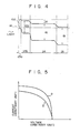
- Fig. 4 is an energy band diagram of the p-i-n type solar cell of Fig. 3. As is evident from Fig. 4, the Eg 15b of the second p-sublayer 23b is set greater than Eg 15a of the first p-sublayer 23a.
- Table 1 below shows the comparison data of the short circuit current density Jsc and conversion efficiency n which were obtained from the p-layer 23 (Example 1) comprised of a first p-sublayer 23a having an Eg of 1.6 eV and a second p-sublayer 23b having an Eg of 1.8 eV, a p-layer (control 1) comprised of a single layer having an Eg of 1.6 eV and a p-layer (control 2) comprised of a single layer having an Eg of 1.8 eV.
- the film thickness of the p-layer was so selected that the Voc is 0.8 V.
- the solar cell of this invention exhibits an excellent performance over that of the conventional solar cell.
- Fig. 5 shows the I-V characteristic of the solar cells.
- the curve a corresponds to the solar cell of Example 1 and the curve b corresponds to the solar cell of Control 2. From the graph of Fig. 5 it can be seen that the solar cell of this invention has a higher current and voltage than the conventional solar cell.
- Table 2 shows the comparison data of the various characteristics of solar cells according to Examples 2 to 4 and Control 3 when the Eg of the first and second p-sublayers was varied in a variety of ways.
- an n-layer may be constructed of a plurality of sublayers each having a different Eg with the n-layer on the light-incident side.
- a first n-sublayer have a thickness of 2 to 5 nm (20 to 50 A) and an Eg of 1.6 to 2.0 eV and that a second n-sublayer have a thickness of 5 to 10 nm (50 to 100 A) and an Eg of 1.7 to 2.1 eV.
- the hydrogenated a-Si layer structure Although Examples using the hydrogenated a-Si layer structure have been explained, it is also possible to use a hydrogenated a-SiC layer structure. In this case, it is also possible to use an a-Si layer as the first p-sublayer and an a-SiC layer as the second p-sublayer. It should be noted that the hydrogenated a-SiC can be readily formed by decomposing a gaseous mixture of SiH 4 and hydrocarbon gas, such as CH 4 and C 2 H 4 by glow discharge.
- the first p-sublayer have a thickness of 2 to 5 nm (20 to 50 A) and an Eg of 1.7 to 2.2 eV
- the second p-sublayer have a thickness of 5 to 10 nm (50 to 100 A) and an Eg of 1.8 to 2.4 eV
- the first n-sublayer have a thickness of 2 to 5 nm (20 to 50 A) and an Eg of 1.7 to 2.2 Ev
- the second n-sublayer have a thickness of 5 to 10 nm (50 to 100 A) and an Eg of 1.8 to 2.4 eV.
- a layer structure having three or more sublayers may be provided in which their Eg's are gradually increased toward the i-layer side.
Landscapes
- Photovoltaic Devices (AREA)
Claims (14)
Applications Claiming Priority (2)
| Application Number | Priority Date | Filing Date | Title |
|---|---|---|---|
| JP57122940A JPS5914679A (ja) | 1982-07-16 | 1982-07-16 | 光起電力装置 |
| JP122940/82 | 1982-07-16 |
Publications (3)
| Publication Number | Publication Date |
|---|---|
| EP0099720A2 EP0099720A2 (de) | 1984-02-01 |
| EP0099720A3 EP0099720A3 (en) | 1985-05-15 |
| EP0099720B1 true EP0099720B1 (de) | 1988-05-18 |
Family
ID=14848370
Family Applications (1)
| Application Number | Title | Priority Date | Filing Date |
|---|---|---|---|
| EP83304053A Expired EP0099720B1 (de) | 1982-07-16 | 1983-07-12 | Fotovoltaische Vorrichtung |
Country Status (4)
| Country | Link |
|---|---|
| US (1) | US4500744A (de) |
| EP (1) | EP0099720B1 (de) |
| JP (1) | JPS5914679A (de) |
| DE (1) | DE3376714D1 (de) |
Families Citing this family (16)
| Publication number | Priority date | Publication date | Assignee | Title |
|---|---|---|---|---|
| JPH0620147B2 (ja) * | 1984-05-11 | 1994-03-16 | 三洋電機株式会社 | 光起電力装置 |
| JPS61222278A (ja) * | 1985-03-28 | 1986-10-02 | Sanyo Electric Co Ltd | 光起電力装置 |
| CA1321660C (en) * | 1985-11-05 | 1993-08-24 | Hideo Yamagishi | Amorphous-containing semiconductor device with high resistivity interlayer or with highly doped interlayer |
| JP2545066B2 (ja) * | 1985-11-14 | 1996-10-16 | 鐘淵化学工業株式会社 | 半導体装置 |
| US4718947A (en) * | 1986-04-17 | 1988-01-12 | Solarex Corporation | Superlattice doped layers for amorphous silicon photovoltaic cells |
| JPS6384075A (ja) * | 1986-09-26 | 1988-04-14 | Sanyo Electric Co Ltd | 光起電力装置 |
| JPH0752778B2 (ja) * | 1987-09-14 | 1995-06-05 | 三洋電機株式会社 | 光起電力装置 |
| JPH068703B2 (ja) * | 1987-11-13 | 1994-02-02 | 株式会社東芝 | 空気調和装置 |
| US5117114A (en) * | 1989-12-11 | 1992-05-26 | The Regents Of The University Of California | High resolution amorphous silicon radiation detectors |
| US5055141A (en) * | 1990-01-19 | 1991-10-08 | Solarex Corporation | Enhancement of short-circuit current by use of wide bandgap n-layers in p-i-n amorphous silicon photovoltaic cells |
| JP2729707B2 (ja) * | 1991-03-27 | 1998-03-18 | 極東工業株式会社 | 建築設備の吊設支持構造 |
| EP0886325A1 (de) * | 1997-06-18 | 1998-12-23 | Rijksuniversiteit Utrecht | Photovoltaische Anordnungen aus amorphem Silizium und Herstellungsverfahren |
| US6383898B1 (en) * | 1999-05-28 | 2002-05-07 | Sharp Kabushiki Kaisha | Method for manufacturing photoelectric conversion device |
| US7667133B2 (en) * | 2003-10-29 | 2010-02-23 | The University Of Toledo | Hybrid window layer for photovoltaic cells |
| DE102008014260A1 (de) * | 2008-03-13 | 2009-09-24 | Schott Solar Gmbh | Silizium-Solarzelle |
| US20110155229A1 (en) * | 2009-12-30 | 2011-06-30 | Du Pont Apollo Ltd. | Solar cell and method for manufacturing the same |
Family Cites Families (3)
| Publication number | Priority date | Publication date | Assignee | Title |
|---|---|---|---|---|
| JPS5688377A (en) * | 1979-12-19 | 1981-07-17 | Mitsubishi Electric Corp | Solar battery and manufacture thereof |
| JPS56150876A (en) * | 1980-04-24 | 1981-11-21 | Sanyo Electric Co Ltd | Photovoltaic device |
| IE52207B1 (en) * | 1980-09-09 | 1987-08-05 | Energy Conversion Devices Inc | Method of grading the band gaps of amorphous alloys and devices |
-
1982
- 1982-07-16 JP JP57122940A patent/JPS5914679A/ja active Pending
-
1983
- 1983-07-12 EP EP83304053A patent/EP0099720B1/de not_active Expired
- 1983-07-12 DE DE8383304053T patent/DE3376714D1/de not_active Expired
- 1983-07-13 US US06/513,390 patent/US4500744A/en not_active Expired - Lifetime
Non-Patent Citations (1)
| Title |
|---|
| IEEE ELECTRON DEVICE LETTERS, vol. EDL-3, no. 5, May 1982, NEW YORK (US), pages 114-115, H. IIDA et al.: "High efficiency a-Si: H p-i-n solar cell using a SnO2/glass substrate" * |
Also Published As
| Publication number | Publication date |
|---|---|
| DE3376714D1 (en) | 1988-06-23 |
| JPS5914679A (ja) | 1984-01-25 |
| EP0099720A3 (en) | 1985-05-15 |
| US4500744A (en) | 1985-02-19 |
| EP0099720A2 (de) | 1984-02-01 |
Similar Documents
| Publication | Publication Date | Title |
|---|---|---|
| US4496788A (en) | Photovoltaic device | |
| US7030413B2 (en) | Photovoltaic device with intrinsic amorphous film at junction, having varied optical band gap through thickness thereof | |
| EP1724840B1 (de) | Photoelektrische zelle | |
| US6121541A (en) | Monolithic multi-junction solar cells with amorphous silicon and CIS and their alloys | |
| US8872020B2 (en) | Heterojunction solar cell based on epitaxial crystalline-silicon thin film on metallurgical silicon substrate design | |
| EP0523919B1 (de) | Photovoltische Vorrichtung mit mehreren Übergängen und Herstellungsverfahren | |
| US7879644B2 (en) | Hybrid window layer for photovoltaic cells | |
| Carlson et al. | Solar cells using discharge-produced amorphous silicon | |
| JP2814351B2 (ja) | 光電装置 | |
| EP0099720B1 (de) | Fotovoltaische Vorrichtung | |
| JP2846651B2 (ja) | 光起電力装置 | |
| US4398054A (en) | Compensated amorphous silicon solar cell incorporating an insulating layer | |
| JPS6249672A (ja) | アモルフアス光起電力素子 | |
| JPH0795603B2 (ja) | 光起電力装置 | |
| US4926230A (en) | Multiple junction solar power generation cells | |
| JP2719036B2 (ja) | 非晶質光電変換装置およびその製造方法 | |
| US4857115A (en) | Photovoltaic device | |
| EP3349257B1 (de) | Verfahren zur herstellung einer solarzelle | |
| US4672148A (en) | Thin-film solar cells | |
| JP2632740B2 (ja) | 非晶質半導体太陽電池 | |
| JP2958491B2 (ja) | 光電変換装置の製造方法 | |
| US8859321B2 (en) | Mixed temperature deposition of thin film silicon tandem cells | |
| JPH0685291A (ja) | 半導体装置およびその製造法 | |
| Arya | High Efficiency Amorphous Silicon Based Solar Cells: A Review | |
| JP3088252B2 (ja) | 非晶質太陽電池 |
Legal Events
| Date | Code | Title | Description |
|---|---|---|---|
| PUAI | Public reference made under article 153(3) epc to a published international application that has entered the european phase |
Free format text: ORIGINAL CODE: 0009012 |
|
| 17P | Request for examination filed |
Effective date: 19830721 |
|
| AK | Designated contracting states |
Designated state(s): DE FR GB NL |
|
| RAP1 | Party data changed (applicant data changed or rights of an application transferred) |
Owner name: KABUSHIKI KAISHA TOSHIBA |
|
| PUAL | Search report despatched |
Free format text: ORIGINAL CODE: 0009013 |
|
| AK | Designated contracting states |
Designated state(s): DE FR GB NL |
|
| 17Q | First examination report despatched |
Effective date: 19860930 |
|
| GRAA | (expected) grant |
Free format text: ORIGINAL CODE: 0009210 |
|
| AK | Designated contracting states |
Kind code of ref document: B1 Designated state(s): DE FR GB NL |
|
| PG25 | Lapsed in a contracting state [announced via postgrant information from national office to epo] |
Ref country code: NL Effective date: 19880518 |
|
| REF | Corresponds to: |
Ref document number: 3376714 Country of ref document: DE Date of ref document: 19880623 |
|
| ET | Fr: translation filed | ||
| PG25 | Lapsed in a contracting state [announced via postgrant information from national office to epo] |
Ref country code: GB Effective date: 19880718 |
|
| NLV1 | Nl: lapsed or annulled due to failure to fulfill the requirements of art. 29p and 29m of the patents act | ||
| PLBE | No opposition filed within time limit |
Free format text: ORIGINAL CODE: 0009261 |
|
| STAA | Information on the status of an ep patent application or granted ep patent |
Free format text: STATUS: NO OPPOSITION FILED WITHIN TIME LIMIT |
|
| GBPC | Gb: european patent ceased through non-payment of renewal fee | ||
| PG25 | Lapsed in a contracting state [announced via postgrant information from national office to epo] |
Ref country code: DE Effective date: 19890401 |
|
| 26N | No opposition filed | ||
| PGFP | Annual fee paid to national office [announced via postgrant information from national office to epo] |
Ref country code: FR Payment date: 19970709 Year of fee payment: 15 |
|
| PG25 | Lapsed in a contracting state [announced via postgrant information from national office to epo] |
Ref country code: FR Free format text: LAPSE BECAUSE OF NON-PAYMENT OF DUE FEES Effective date: 19990331 |
|
| REG | Reference to a national code |
Ref country code: FR Ref legal event code: ST |