EP0096885B1 - Synchronisationskreis zur Detektierung und Interpolation von Synchronisationssignalen, welche in Digitalsignalen enthalten sind - Google Patents
Synchronisationskreis zur Detektierung und Interpolation von Synchronisationssignalen, welche in Digitalsignalen enthalten sind Download PDFInfo
- Publication number
- EP0096885B1 EP0096885B1 EP83105807A EP83105807A EP0096885B1 EP 0096885 B1 EP0096885 B1 EP 0096885B1 EP 83105807 A EP83105807 A EP 83105807A EP 83105807 A EP83105807 A EP 83105807A EP 0096885 B1 EP0096885 B1 EP 0096885B1
- Authority
- EP
- European Patent Office
- Prior art keywords
- output signal
- signal
- sync
- output
- circuit
- Prior art date
- Legal status (The legal status is an assumption and is not a legal conclusion. Google has not performed a legal analysis and makes no representation as to the accuracy of the status listed.)
- Expired
Links
Images


Classifications
-
- G—PHYSICS
- G11—INFORMATION STORAGE
- G11B—INFORMATION STORAGE BASED ON RELATIVE MOVEMENT BETWEEN RECORD CARRIER AND TRANSDUCER
- G11B5/00—Recording by magnetisation or demagnetisation of a record carrier; Reproducing by magnetic means; Record carriers therefor
- G11B5/02—Recording, reproducing, or erasing methods; Read, write or erase circuits therefor
- G11B5/09—Digital recording
-
- G—PHYSICS
- G11—INFORMATION STORAGE
- G11B—INFORMATION STORAGE BASED ON RELATIVE MOVEMENT BETWEEN RECORD CARRIER AND TRANSDUCER
- G11B20/00—Signal processing not specific to the method of recording or reproducing; Circuits therefor
- G11B20/10—Digital recording or reproducing
- G11B20/14—Digital recording or reproducing using self-clocking codes
- G11B20/1403—Digital recording or reproducing using self-clocking codes characterised by the use of two levels
-
- G—PHYSICS
- G11—INFORMATION STORAGE
- G11B—INFORMATION STORAGE BASED ON RELATIVE MOVEMENT BETWEEN RECORD CARRIER AND TRANSDUCER
- G11B20/00—Signal processing not specific to the method of recording or reproducing; Circuits therefor
- G11B20/10—Digital recording or reproducing
- G11B20/10527—Audio or video recording; Data buffering arrangements
-
- G—PHYSICS
- G11—INFORMATION STORAGE
- G11B—INFORMATION STORAGE BASED ON RELATIVE MOVEMENT BETWEEN RECORD CARRIER AND TRANSDUCER
- G11B27/00—Editing; Indexing; Addressing; Timing or synchronising; Monitoring; Measuring tape travel
- G11B27/10—Indexing; Addressing; Timing or synchronising; Measuring tape travel
- G11B27/19—Indexing; Addressing; Timing or synchronising; Measuring tape travel by using information detectable on the record carrier
- G11B27/28—Indexing; Addressing; Timing or synchronising; Measuring tape travel by using information detectable on the record carrier by using information signals recorded by the same method as the main recording
- G11B27/30—Indexing; Addressing; Timing or synchronising; Measuring tape travel by using information detectable on the record carrier by using information signals recorded by the same method as the main recording on the same track as the main recording
- G11B27/3027—Indexing; Addressing; Timing or synchronising; Measuring tape travel by using information detectable on the record carrier by using information signals recorded by the same method as the main recording on the same track as the main recording used signal is digitally coded
Definitions
- the present invention relates to a synchronizing circuit for detecting sync signals contained in a digital input signal and for properly protecting the synchronization when the sync signals drop out.
- Digital audio systems have been recently developed because an audio reproduction of high quality can be achieved.
- the digital audio systems are grouped into a system which uses a magnetic tape and a system which uses a disc.
- a compact disc (CD) system in which digital data recorded on a compact disc are optically read out by a laser beam has been developed and put into practical use.
- digital data are subjected to an EF (eight- bit to fourteen-bit) modulation arranged in one frame in a given format to be recorded on a disc.
- One frame of digital data includes a frame sync signal disposed at the head of the frame, a plurality of audio data words, and error correcting bits and consists of 588 channel bits in total.
- the sync signal consists of 24 channel bits and has a specific variation pattern sufficient to be distinguished from any other digital data.
- the frame sync signals are used for generating control signals for dividing frames and dividing digital data in one frame at a given unit.
- the playback apparatus is provided with a sync signal detecting circuit.
- a sync protecting circuit is further used in combination with the sync signal detecting circuit for interpolating sync signals when the sync signals drop out due to scratches on a disc.
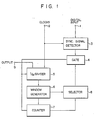
- Fig. 1 shows a prior sync circuit containing the sync signal detecting circuit and the sync protecting circuit
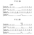
- Figs. 2A and 2B are timing diagrams for explaining the operation of the sync circuit of Fig. 1.
- a digital input signal applied to an input terminal 1 and having N bits per frame is applied to a sync signal detecting circuit 3, together with a clock signal generated on the basis of an output signal of a PLL circuit for detecting clock components contained in the digital signal reproduced from a disc, thereby to detect a frame sync signal for each frame.
- the output of sync signal detecting circuit 3 is connected to a gate circuit 4.
- the output of gate circuit 4 is connected to a clear terminal of a 1/N frequency divider (scale-of-N counter) for frequency-dividing the clock signal.
- the output of 1/N frequency divider 5 is connected to a window generator 6 of which the output is connected to a counter 7 which is cleared by an output signal of gate circuit 4.
- a selector 8 couples the output of window generator 6 or the counter 7 to a control terminal of gate circuit 4.
- the output of 1/N frequency divider 5 is connected to an output terminal 9.
- sync signal detecting circuit 3 detects the sync signal contained in each frame of the input signal and outputs a detect signal to gate circuit 4.
- Gate circuit 4 controls the supply of the sync detect signal from sync signal detecting circuit 3 to 1/N frequency divider 5 according to an output signal of selector 8. Frequency divider 5 is cleared every time an output signal of gate circuit 4 becomes high to provide a frame sync control signal to output terminal 9 for every N bits of the clock signal.
- Window generator 6 increases its output during a period of several bits in and near the N-th bit at which the next frame sync control signal is to be produced starting from a bit at which a frame sync control signal is produced by frequency divider 5, that is to say, generates a window to make gate circuit 4 conductive through selector 8.
- selector 8 applies a window output of window generator 6 to gate circuit 4 to apply an output signal of sync signal detecting circuit 3 to frequency divider 5, through a window corresponding to the sync signal of the preceding frame. Owing to this operation, an erroneous operation due to noise other than true sync detect signals can be prevented.
- the prior art sync circuit has a disadvantage in that, when some sync signals drop out due to some cause, erroneous sync control signals may be formed by the influence of noise so that the synchronizing operation of a digital signal processing circuit is lost.
- the object of the present invention is to provide a synchronizing circuit for detecting sync signals and protecting synchronizing in a device for processing a digital signal including a plurality of frames each having a frame sync signal, which is arranged to quickly restore the synchronization after noise is detected as a sync signal.
- the synchronizing circuit comprises the features of claim 1.
- the synchronizing circuit comprises the features of claim 2.
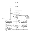
- Digital data recorded on a disc 113 mounted on a turntable 121 driven by a disc motor 111 is picked up by an optical pick-up device 114 as shown in Fig. 3.
- Optical pick-up device 114 irradiates the recording surface of disc 113 with a laser beam emitted from a semi-conductor laser 114a through a beam splitter 114b and an objective lens 114c.
- a laser beam reflected from pits formed on disc 113 which represent PCM digital data containing EF modulated and interleaved audio information signals is guided through objective lens 114c and beam splitter 114b to a four- photodetector unit 114d to produce four reproduced signals.
- the pick-up device is rectilinearly driven in the radial direction of disc 113 by means of a feed motor 115.
- the four output signals of photodetector unit 114d are applied to a matrix circuit 116 to produce a focus error signal F, a tracking error signal T and a high frequency signal (modulated digital data) RF.
- the focus error signal F together with a focus search signal from a focus search circuit 110, is applied to a focus servo system FS of optical pick-up device 114.
- the tracking error signal T together with a search control signal applied from a system controller 117, is applied to a tracking servo system TS of pick-up device 114 and to feed motor 115, thereby to perform a linear tracking control of the pick-up device.
- the high frequency signal RF is applied as a main data component to a data processing system 118.
- modulated digital data RF is led to a wave shaper circuit 120 controlled by a slice level (eye pattern) detector 119, where analog components are removed to extract only digital data components.
- the data components are applied to a synchronizing clock reproducing circuit 121 of PLL type and to an edge detector 122a of a first signal processing system 122.
- a sync clock signal from sync clock reproducing circuit 121 is applied to a sync signal separation clock generating circuit 122b in first signal processing system 122, thereby forming a clock signal for sync signal separation.
- Edge detector 122a detects edges (change points) of the high frequency signal RF which has been formed by NRZI modulating the EF modulated data (NRZ) to recover the EF modulated data.
- An output signal of edge detector 122a is led to a sync signal detector circuit 122c where the sync signals are detected using the clock signal from clock generator 122b.
- the output signal of edge detector is also applied to a demodulator circuit 122d where the respective EF modulated data are demodulated to the original bit number.
- a sync detect signal from sync signal detector circuit 122c is applied through a sync protecting circuit 122e to a timing circuit 122f for generating timing signals for processing input data, together with clocks from clock generator 122b.
- Sync protecting circuit 122e interpolates sync signals for preventing an erroneous operation when sync signals are not detected by sync signal detector circuit 122c.
- a demodulated signal from demodulator circuit 122d is applied to an input/output control circuit 123a of a second signal processing system 123 to be described later, through a data bus input/ output control circuit 122g.
- a control signal as a subcode and a display signal component in the demodulated signal are applied to a control display processing circuit 122h and a subcode processing circuit 122i.
- the subcode data which has been subjected to error detection and correction, is applied through an interface circuit 122q to a system controller 117.
- System controller 117 is provided with a microcomputer, an interface circuit and a driver integrated circuit. System controller 117 controls the playback device to a desired state by a command given by control switches 124 and causes a display 125 to display the subcode, e.g. index data of reproduced music.
- a timing signal from a timing signal generator circuit 122f controls input/output control circuit 122g through a data select circuit 122j, and is applied to a frequency detector 122k and a phase detector 1221 to perform an automatic frequency control (AFC) and an automatic phase control (APC) for driving a disc motor 111 at a constant linear velocity (CLV) through PWM modulator 122m.
- a system clock generated by a system clock generator circuit 122p driven by a crystal oscillator 122n is applied to phase detector 1221.
- the output data of input/output control circuit 123a of second signal processing system 123 is applied to syndrome detector 123b, error pointer control circuit 123c, error correct circuit 123d, and output circuit 123e.
- Syndrome detector 123b detects an error of data words and error correct circuit 123d corrects erroneous data words.
- Output circuit 123e is arranged to perform data interpolation as required.
- An output signal of output circuit 123e is converted into an analog signal by digital-to-analog (D/A) converter 126.
- An external memory control circuit 123f cooperates with data selector circuit 122j to control external memory 127 storing data necessary for error correction to fetch data neccessary for error correction through input/output control circuit 123a.
- Timing control circuit 123g receives a system clock from system clock generating circuit 122p to generate timing control signals necessary for error correction, interpolation and D/A conversion.
- a muting control circuit 123h controls output circuit 123e at the time of error correction and at the start and end of playback under the control of an output signal from error pointer control circuit 123c or a signal from system controller 117 to perform a muting operation.
- Audio signals produced by D/A converter 126 drive a speaker 130 through a low pass filter (LPF) 128 and an amplifier 129.
- LPF low pass filter
- Fig. 4 like numerals are used for designating like or equivalent portions in Fig. 1.
- the sync circuit is constructed so as to add a gate circuit 10, a 1/N frequency divider 11, a window generator 12 and an OR gate 13 to the prior art sync circuit of Fig. 1.
- the output of sync signal detecting circuit 3 is connected to gate circuit 10 which is enabled when the output signal of counter 7 is high.
- the output signal of gate circuit 10 is connected through OR gate 13 to a clear terminal of 1/N frequency divider (scale-of-N counter) 11 for frequency-dividing the clock signal.
- the output signal of gate circuit 4 is connected to a clear terminal of frequency divider 11 through OR gate 13.
- the output of frequency divider 11 is connected to window generator 12 whose output is connected to selector 8. Selector 8 is so arranged as to, when the output of counter 7 is low, couple the output of window generator 6 to gate circuit 4 and, when the output of counter 7 is high, couple the output of window generator 12 to gate circuit 4.
- sync signal detector circuit 3 detects for every frame the sync signal contained in the input signal and applies a sync detect signal to first and second gate circuits 4 and 10.
- Frequency divider (first counter) 5 is cleared every time the output of gate circuit 4 goes high to send a sync control signal to output terminal 9.
- the output of first window generator 6 goes high during several bits in and near the N-th bit at which the next frame sync control signal is to be produced after frequency divider 5 produces a frame sync control signal.
- the output signal of window generator 6 is applied to gate circuit 4 through selector 8.
- counter (second counter) 7 is counted up every frame by the window generator 6.
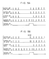
- counter 7 counts a preset number of frames e.g. four frames, its output becomes high, as indicated in Fig. 5A.
- the output of second window generator 12 is coupled to gate circuit 4 and gate circuit 10 is enabled.
- frequency divider (third counter) 11 is cleared by an output signal of gate circuit 4 through OR gate 13 and thus synchronized with frequency divider 5.
- frequency divider 11 is cleared by the output signal of sync signal detecting circuit 3 through gate circuit 10 and OR gate 13.
- window generator 12 will go high during several bits in and near the N-th bit counted from this time to enable gate 4. Accordingly, when an output signal which is first produced from sync signal detector circuit 3 and clears divider 11, as shown in Fig. 5A, is a sync signal, a sync detect signal next produced from sync signal detector 3 is derived from gate circuit 4 to clear frequency divider 5 and counter 7. For this reason, succeeding sync detect signals produced by sync signal detecting circuit 3 are derived from gate circuit 4 enabled every frame by window generator 6 so that synchronization is established between sync signal detector circuit 3 and frequency divider 5.
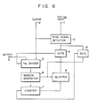
- Fig. 6 shows another embodiment of the sync circuit of the present invention, in which like reference numerals are used to designate like or equivalent portions in Fig. 1.
- the sync circuit of this embodiment is provided with gate circuit 10 in the prior art sync circuit.
- Gate circuit 10 is enabled by a window output of window generator 6 to clear counter 7 by an output signal of sync signal detecting circuit 3.
- sync signal detector circuit 3 detects the sync signal contained in each frame of the input signal and applies the detect signal to first and second gate circuits 4 and 10.
- Frequency divider 5 is cleared every time the output signal of gate circuit 4 goes high and sends a sync detect signal to output terminal 9.
- the output signal of window generator 6 goes high during several bits in and near the N-th bit at which frequency divider 5 should produce the next frame sync control signal.
- the window output is coupled to gate circuit 4 through selector 8.
- sync signal detecting circuit 3 is normally synchronized with frequency divider 6, the output of gate circuit 4 goes high only when an output signal of sync signal detecting circuit 3 falls within a window formed by window generator 6.
- counter 7 is cleared every frame by an output signal of sync signal detector circuit 3 through gate circuit 10.
- the first output signal of sync detector circuit 3 is noise and thereafter sync signals are normally detected after the output of counter 7 has become high, then frequency divider 5 will be cleared by the noise output, but counter 7 will not be cleared.
- the sync detect signals are successively produced by sync signal detecting circuit 3 after the noise output is produced, the first detect signal clears frequency divider 5, but does not clear counter 7 since gate circuit 10 is not enabled.
- gate circuit 10 has been enabled by an output signal of window generator 6. Accordingly, frequency divider 5 and counter 7 are cleared by the second detect signal through gate circuits 4 and 10, respectively. For this reason, gate circuit 4 is then enabled every frame by the output signal of window generator 6 and the synchronization between sync signal detecting circuit and frequency divider 5 is restored.
Landscapes
- Engineering & Computer Science (AREA)
- Signal Processing (AREA)
- Multimedia (AREA)
- Signal Processing For Digital Recording And Reproducing (AREA)
- Synchronisation In Digital Transmission Systems (AREA)
Claims (2)
Applications Claiming Priority (4)
| Application Number | Priority Date | Filing Date | Title |
|---|---|---|---|
| JP10282982A JPS58219828A (ja) | 1982-06-15 | 1982-06-15 | 同期回路 |
| JP102838/82 | 1982-06-15 | ||
| JP102829/82 | 1982-06-15 | ||
| JP10283882A JPS58220227A (ja) | 1982-06-15 | 1982-06-15 | 同期回路 |
Publications (2)
| Publication Number | Publication Date |
|---|---|
| EP0096885A1 EP0096885A1 (de) | 1983-12-28 |
| EP0096885B1 true EP0096885B1 (de) | 1985-09-11 |
Family
ID=26443509
Family Applications (1)
| Application Number | Title | Priority Date | Filing Date |
|---|---|---|---|
| EP83105807A Expired EP0096885B1 (de) | 1982-06-15 | 1983-06-14 | Synchronisationskreis zur Detektierung und Interpolation von Synchronisationssignalen, welche in Digitalsignalen enthalten sind |
Country Status (4)
| Country | Link |
|---|---|
| US (1) | US4453260A (de) |
| EP (1) | EP0096885B1 (de) |
| KR (1) | KR870000190B1 (de) |
| DE (1) | DE3360787D1 (de) |
Families Citing this family (28)
| Publication number | Priority date | Publication date | Assignee | Title |
|---|---|---|---|---|
| JPS59117838A (ja) * | 1982-12-24 | 1984-07-07 | Sony Corp | マ−カ−信号検出回路 |
| FR2548490A1 (fr) * | 1983-06-30 | 1985-01-04 | Thomson Csf | Circuit programmable de transformation serie-parallele d'un signal numerique, et son application a un recepteur de signaux video numeriques |
| JPS60164980A (ja) * | 1984-02-06 | 1985-08-28 | Mitsubishi Electric Corp | 光デイスク制御装置 |
| JP2565184B2 (ja) * | 1985-02-28 | 1996-12-18 | ソニー株式会社 | 信号選択回路 |
| US4731676A (en) * | 1985-12-13 | 1988-03-15 | Cyclotomics, Inc. | Transparent synchronization of multiple channel data |
| GB2187366B (en) * | 1986-02-27 | 1989-11-08 | Sony Corp | Synchronizing signal decoding |
| NZ220548A (en) * | 1986-06-18 | 1990-05-28 | Fujitsu Ltd | Tdm frame synchronising circuit |
| US4716578A (en) * | 1986-09-29 | 1987-12-29 | Northern Telecom Limited | Circuit and method for the recovery of data from a digital data stream |
| GB8705771D0 (en) * | 1987-03-11 | 1987-04-15 | Plessey Co Plc | Synchronisation arrangements |
| JPH01144738A (ja) * | 1987-11-30 | 1989-06-07 | Nec Home Electron Ltd | ウインドウ法同期保護回路 |
| JP2712212B2 (ja) * | 1987-12-23 | 1998-02-10 | ソニー株式会社 | 同期信号の検出及び保護回路 |
| KR910003232B1 (ko) * | 1988-03-29 | 1991-05-24 | 삼성전자 주식회사 | 페이징 수신기의 데이타 수신클럭 발생방법 |
| US4831439A (en) * | 1988-05-16 | 1989-05-16 | General Electric Company | Refresh system for digital signals with refresh cycle synchronization |
| US5252963A (en) * | 1990-01-04 | 1993-10-12 | Motorola, Inc. | "Selective call receiver" |
| JPH05160825A (ja) * | 1991-12-03 | 1993-06-25 | Fujitsu Ltd | 同期回路 |
| JP2606090B2 (ja) * | 1993-07-14 | 1997-04-30 | 日本電気株式会社 | 光学的情報制御装置 |
| KR0157585B1 (ko) * | 1993-09-24 | 1998-12-15 | 김광호 | 디스크재생장치의 동기내삽회로 및 동기상태검출회로 |
| KR0148181B1 (ko) * | 1995-03-31 | 1998-10-15 | 김광호 | 디지탈 기록재생시스템의 가변적 동기패턴검출장치 및 방법 |
| US5793548A (en) * | 1995-05-12 | 1998-08-11 | Cirrus Logic, Inc. | Fault tolerant sync mark detector for comparing a sign and magnitude of a detected sequence to a target sync mark in sampled amplitude magnetic recording |
| KR100258332B1 (ko) * | 1997-12-26 | 2000-06-01 | 윤종용 | 싱크검출장치와 그에 따른 광 디스크 재생장치 |
| US6631483B1 (en) | 1999-06-08 | 2003-10-07 | Cisco Technology, Inc. | Clock synchronization and fault protection for a telecommunications device |
| US6683848B1 (en) * | 1999-06-08 | 2004-01-27 | Cisco Technology, Inc. | Frame synchronization and fault protection for a telecommunications device |
| US7350116B1 (en) | 1999-06-08 | 2008-03-25 | Cisco Technology, Inc. | Clock synchronization and fault protection for a telecommunications device |
| US6901127B1 (en) * | 2000-04-26 | 2005-05-31 | Sigmatel, Inc. | Method and apparatus for data recovery |
| JP3715623B2 (ja) * | 2002-12-25 | 2005-11-09 | 株式会社東芝 | 同期信号検出装置及び同期信号検出方法 |
| JP3958269B2 (ja) * | 2003-09-09 | 2007-08-15 | 日本テキサス・インスツルメンツ株式会社 | 復調装置およびこれを有するデータ記録装置 |
| DE102004060044A1 (de) * | 2004-12-14 | 2006-06-29 | Lanxess Deutschland Gmbh | Farbstarke, reduktions- und oxidationsstabile Eisenoxidschwarzpigmente zur Einfärbung von Kunst- und Baustoffen |
| US8085009B2 (en) * | 2007-08-13 | 2011-12-27 | The Powerwise Group, Inc. | IGBT/FET-based energy savings device for reducing a predetermined amount of voltage using pulse width modulation |
Family Cites Families (4)
| Publication number | Priority date | Publication date | Assignee | Title |
|---|---|---|---|---|
| JPS5528580B2 (de) * | 1974-06-13 | 1980-07-29 | ||
| JPS5580867A (en) * | 1978-12-12 | 1980-06-18 | Sony Corp | Block synchronous signal extracting circuit |
| JPS55107360A (en) * | 1979-02-08 | 1980-08-18 | Matsushita Electric Ind Co Ltd | Detector for synchronizing signal |
| NL7903284A (nl) * | 1979-04-26 | 1980-10-28 | Philips Nv | Werkwijze voor framesynchronisatie van een digitaal tdm communicatiestelsel en inrichting voor het uitvoeren van de werkwijze. |
-
1982
- 1982-09-27 US US06/423,725 patent/US4453260A/en not_active Expired - Lifetime
-
1983
- 1983-03-19 KR KR8301137A patent/KR870000190B1/ko not_active IP Right Cessation
- 1983-06-14 EP EP83105807A patent/EP0096885B1/de not_active Expired
- 1983-06-14 DE DE8383105807T patent/DE3360787D1/de not_active Expired
Also Published As
| Publication number | Publication date |
|---|---|
| US4453260A (en) | 1984-06-05 |
| KR840004282A (ko) | 1984-10-10 |
| KR870000190B1 (en) | 1987-02-14 |
| EP0096885A1 (de) | 1983-12-28 |
| DE3360787D1 (en) | 1985-10-17 |
Similar Documents
| Publication | Publication Date | Title |
|---|---|---|
| EP0096885B1 (de) | Synchronisationskreis zur Detektierung und Interpolation von Synchronisationssignalen, welche in Digitalsignalen enthalten sind | |
| AU613292B2 (en) | Method of and apparatus for recording an information signal | |
| EP0098349B1 (de) | Frequenzdetektorschaltung für ein digitales Informationswiedergabesystem | |
| EP0096106B1 (de) | PLL-Steuerkreis | |
| EP0096162B1 (de) | Schalteinrichtung zur Steuerung des Motors eines Datenwiedergabegeräts | |
| JP2819294B2 (ja) | デジタル情報再生装置 | |
| JP2712212B2 (ja) | 同期信号の検出及び保護回路 | |
| KR100276199B1 (ko) | 디스크 재생 장치 및 데이타 슬라이스 회로 | |
| JPH10257041A (ja) | フェイズロックドループ回路及び再生装置 | |
| US6665246B2 (en) | Optical disk apparatus | |
| JPS59111423A (ja) | 同期信号再生用pll回路の保護装置 | |
| JPH0574147B2 (de) | ||
| JPH0150992B2 (de) | ||
| EP1190570B1 (de) | Aufnahme/wiedergabe-anlage mit schreibvorrichtung zum aufnehmen und/oder lesevorrichtung und detektorvorrichtung zur wiedergabe von einem informationssignal in bzw. von mindestens einer spur auf einem aufnahmeträger | |
| JPH0227754B2 (ja) | Dokishingokenshutsukairo | |
| JPS58220271A (ja) | デジタルデイスクプレ−ヤのモ−タ制御装置 | |
| JP4264540B2 (ja) | 再生回路及び同回路を有する光ディスク再生装置 | |
| JP3043209B2 (ja) | 光ディスク装置のスピンドル制御回路 | |
| JPS6310509B2 (de) | ||
| JPS63866B2 (de) | ||
| JPH0411943B2 (de) | ||
| JPH0462152B2 (de) | ||
| JPS6310506B2 (de) | ||
| JPS5921107B2 (ja) | Pcm記録再生装置 | |
| JPS63187461A (ja) | 情報記録ディスク再生装置 |
Legal Events
| Date | Code | Title | Description |
|---|---|---|---|
| PUAI | Public reference made under article 153(3) epc to a published international application that has entered the european phase |
Free format text: ORIGINAL CODE: 0009012 |
|
| 17P | Request for examination filed |
Effective date: 19830614 |
|
| AK | Designated contracting states |
Designated state(s): DE FR GB NL |
|
| RAP1 | Party data changed (applicant data changed or rights of an application transferred) |
Owner name: KABUSHIKI KAISHA TOSHIBA |
|
| GRAA | (expected) grant |
Free format text: ORIGINAL CODE: 0009210 |
|
| AK | Designated contracting states |
Designated state(s): DE FR GB NL |
|
| REF | Corresponds to: |
Ref document number: 3360787 Country of ref document: DE Date of ref document: 19851017 |
|
| ET | Fr: translation filed | ||
| PLBE | No opposition filed within time limit |
Free format text: ORIGINAL CODE: 0009261 |
|
| STAA | Information on the status of an ep patent application or granted ep patent |
Free format text: STATUS: NO OPPOSITION FILED WITHIN TIME LIMIT |
|
| 26N | No opposition filed | ||
| REG | Reference to a national code |
Ref country code: GB Ref legal event code: 746 |
|
| REG | Reference to a national code |
Ref country code: GB Ref legal event code: IF02 |
|
| PGFP | Annual fee paid to national office [announced via postgrant information from national office to epo] |
Ref country code: FR Payment date: 20020610 Year of fee payment: 20 |
|
| PGFP | Annual fee paid to national office [announced via postgrant information from national office to epo] |
Ref country code: GB Payment date: 20020612 Year of fee payment: 20 |
|
| PGFP | Annual fee paid to national office [announced via postgrant information from national office to epo] |
Ref country code: DE Payment date: 20020619 Year of fee payment: 20 |
|
| PGFP | Annual fee paid to national office [announced via postgrant information from national office to epo] |
Ref country code: NL Payment date: 20020628 Year of fee payment: 20 |
|
| PG25 | Lapsed in a contracting state [announced via postgrant information from national office to epo] |
Ref country code: GB Free format text: LAPSE BECAUSE OF EXPIRATION OF PROTECTION Effective date: 20030613 |
|
| PG25 | Lapsed in a contracting state [announced via postgrant information from national office to epo] |
Ref country code: NL Free format text: LAPSE BECAUSE OF EXPIRATION OF PROTECTION Effective date: 20030614 |
|
| REG | Reference to a national code |
Ref country code: GB Ref legal event code: PE20 |
|
| NLV7 | Nl: ceased due to reaching the maximum lifetime of a patent |
Effective date: 20030614 |