EP0093412A1 - Appareil pour la pulvérisation par un magnétronet procédé pour former un film magnétique mince à la surface d'un substrat - Google Patents
Appareil pour la pulvérisation par un magnétronet procédé pour former un film magnétique mince à la surface d'un substrat Download PDFInfo
- Publication number
- EP0093412A1 EP0093412A1 EP83104178A EP83104178A EP0093412A1 EP 0093412 A1 EP0093412 A1 EP 0093412A1 EP 83104178 A EP83104178 A EP 83104178A EP 83104178 A EP83104178 A EP 83104178A EP 0093412 A1 EP0093412 A1 EP 0093412A1
- Authority
- EP
- European Patent Office
- Prior art keywords
- target
- magnetron sputtering
- magnetic field
- sputtering apparatus
- substrate
- Prior art date
- Legal status (The legal status is an assumption and is not a legal conclusion. Google has not performed a legal analysis and makes no representation as to the accuracy of the status listed.)
- Granted
Links
Images


Classifications
-
- H—ELECTRICITY
- H01—ELECTRIC ELEMENTS
- H01J—ELECTRIC DISCHARGE TUBES OR DISCHARGE LAMPS
- H01J37/00—Discharge tubes with provision for introducing objects or material to be exposed to the discharge, e.g. for the purpose of examination or processing thereof
- H01J37/32—Gas-filled discharge tubes
- H01J37/34—Gas-filled discharge tubes operating with cathodic sputtering
- H01J37/3402—Gas-filled discharge tubes operating with cathodic sputtering using supplementary magnetic fields
- H01J37/3405—Magnetron sputtering
Definitions
- a target 1 of 60 mm x 120 mm was located on the upper face of a copper electrode 2.
- Samarium - cobalt magnets 3 of 15.2 mm diameter and 20 mm height were disposed as shown by broken lines in Fig. 3 with the north poles thereof being faced to the underside of the target 1.
- Substantially E-shaped yoke 4 was disposed below the undersides of the magnets and also at the central area of the underside of the target electrode 2.
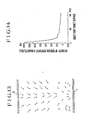
- the direction of the magnetic field produced in the space above the target 1 and the intensity of the vertical component in this magnetic fiels (oersted Oe) are shown in Figs. 5 and 6, respectively.
Applications Claiming Priority (2)
| Application Number | Priority Date | Filing Date | Title |
|---|---|---|---|
| JP57071556A JPS58189372A (ja) | 1982-04-30 | 1982-04-30 | マグネトロンスパツタ装置 |
| JP71556/82 | 1982-04-30 |
Publications (2)
| Publication Number | Publication Date |
|---|---|
| EP0093412A1 true EP0093412A1 (fr) | 1983-11-09 |
| EP0093412B1 EP0093412B1 (fr) | 1987-04-08 |
Family
ID=13464114
Family Applications (1)
| Application Number | Title | Priority Date | Filing Date |
|---|---|---|---|
| EP83104178A Expired EP0093412B1 (fr) | 1982-04-30 | 1983-04-28 | Appareil pour la pulvérisation par un magnétronet procédé pour former un film magnétique mince à la surface d'un substrat |
Country Status (4)
| Country | Link |
|---|---|
| US (1) | US4441974A (fr) |
| EP (1) | EP0093412B1 (fr) |
| JP (1) | JPS58189372A (fr) |
| DE (1) | DE3370830D1 (fr) |
Cited By (2)
| Publication number | Priority date | Publication date | Assignee | Title |
|---|---|---|---|---|
| GB2144772A (en) * | 1983-07-19 | 1985-03-13 | Varian Associates | Magnetron sputter coating source for both magnetic and nonmagnetic target materials |
| EP0416241A2 (fr) * | 1989-09-07 | 1991-03-13 | Leybold Aktiengesellschaft | Dispositif pour le revêtement d'un substrat |
Families Citing this family (34)
| Publication number | Priority date | Publication date | Assignee | Title |
|---|---|---|---|---|
| US4666788A (en) * | 1982-02-16 | 1987-05-19 | Teijin Limited | Perpendicular magnetic recording medium, method for producing the same, and sputtering device |
| US4595482A (en) * | 1984-05-17 | 1986-06-17 | Varian Associates, Inc. | Apparatus for and the method of controlling magnetron sputter device having separate confining magnetic fields to separate targets subject to separate discharges |
| US4606806A (en) * | 1984-05-17 | 1986-08-19 | Varian Associates, Inc. | Magnetron sputter device having planar and curved targets |
| US4657654A (en) * | 1984-05-17 | 1987-04-14 | Varian Associates, Inc. | Targets for magnetron sputter device having separate confining magnetic fields to separate targets subject to separate discharges |
| US4569746A (en) * | 1984-05-17 | 1986-02-11 | Varian Associates, Inc. | Magnetron sputter device using the same pole piece for coupling separate confining magnetic fields to separate targets subject to separate discharges |
| US4892633A (en) * | 1988-11-14 | 1990-01-09 | Vac-Tec Systems, Inc. | Magnetron sputtering cathode |
| US4865708A (en) * | 1988-11-14 | 1989-09-12 | Vac-Tec Systems, Inc. | Magnetron sputtering cathode |
| US5130170A (en) * | 1989-06-28 | 1992-07-14 | Canon Kabushiki Kaisha | Microwave pcvd method for continuously forming a large area functional deposited film using a curved moving substrate web with microwave energy with a directivity in one direction perpendicular to the direction of microwave propagation |
| US5455197A (en) * | 1993-07-16 | 1995-10-03 | Materials Research Corporation | Control of the crystal orientation dependent properties of a film deposited on a semiconductor wafer |
| US5332637A (en) * | 1993-08-31 | 1994-07-26 | Eastman Kodak Company | Electrostatographic dry toner and developer compositions with hydroxyphthalimide |
| US5358815A (en) * | 1993-08-31 | 1994-10-25 | Eastman Kodak Company | Toner compositions containing negative charge-controlling additive |
| US5358818A (en) * | 1993-08-31 | 1994-10-25 | Eastman Kodak Company | Ortho-benzoic sulfimide as charge-controlling agent |
| US5358817A (en) * | 1993-08-31 | 1994-10-25 | Eastman Kodak Company | Toner compositions containing as a negative charge-controlling agent the calcium salt of ortho-benzoic sulfimide |
| US5358814A (en) * | 1993-08-31 | 1994-10-25 | Eastman Kodak Company | Toner compositions containing as a negative charge-controlling agent a mixture of ortho-benzoic sulfimide and para-anisic acid |
| US5358816A (en) * | 1993-08-31 | 1994-10-25 | Eastman Kodak Company | Zinc salt of ortho-benzoic sulfimide as negative charge-controlling additive for toner and developer compositions |
| SE509933C2 (sv) | 1996-09-16 | 1999-03-22 | Scandinavian Solar Ab | Sätt och anordning att framställa ett spektralselektivt absorberande skikt till solkollektorer samt framställt skikt |
| US6093290A (en) | 1997-05-14 | 2000-07-25 | Canon Kabushiki Kaisha | Method of generating a reciprocating plurality of magnetic fluxes on a target |
| US6042700A (en) * | 1997-09-15 | 2000-03-28 | Applied Materials, Inc. | Adjustment of deposition uniformity in an inductively coupled plasma source |
| JP4204978B2 (ja) * | 2001-12-19 | 2009-01-07 | 日鉱金属株式会社 | 磁性体ターゲットとバッキングプレートとの接合方法及び磁性体ターゲット |
| US7205960B2 (en) | 2003-02-19 | 2007-04-17 | Mirage Innovations Ltd. | Chromatic planar optic display system |
| US7297422B2 (en) * | 2003-12-19 | 2007-11-20 | Seagate Technology Llc | Method for sputtering magnetic recording media |
| US7492512B2 (en) * | 2004-07-23 | 2009-02-17 | Mirage International Ltd. | Wide field-of-view binocular device, system and kit |
| US7499216B2 (en) * | 2004-07-23 | 2009-03-03 | Mirage Innovations Ltd. | Wide field-of-view binocular device |
| US7573640B2 (en) * | 2005-04-04 | 2009-08-11 | Mirage Innovations Ltd. | Multi-plane optical apparatus |
| US20080043334A1 (en) * | 2006-08-18 | 2008-02-21 | Mirage Innovations Ltd. | Diffractive optical relay and method for manufacturing the same |
| EP1942364A1 (fr) | 2005-09-14 | 2008-07-09 | Mirage Innovations Ltd. | Relais optique à diffraction et son procédé de fabrication |
| EP1932051A1 (fr) * | 2005-09-14 | 2008-06-18 | Mirage Innovations Ltd. | Réseau de diffraction avec un facteur d'utilisation variant dans l'espace |
| EP1943556B1 (fr) * | 2005-11-03 | 2009-02-11 | Mirage Innovations Ltd. | Dispositif de relais optique binoculaire |
| WO2008023375A1 (fr) * | 2006-08-23 | 2008-02-28 | Mirage Innovations Ltd. | Dispositif de relais optique de diffraction ayant une uniformité de couleur améliorée |
| JP5300084B2 (ja) * | 2007-06-01 | 2013-09-25 | 国立大学法人山口大学 | 薄膜作製用スパッタ装置 |
| US20100302644A1 (en) * | 2007-09-18 | 2010-12-02 | Mirage Innovations Ltd | Slanted optical device |
| JP2012112040A (ja) * | 2010-11-05 | 2012-06-14 | Shin-Etsu Chemical Co Ltd | スパッタ装置用磁気回路 |
| JP5810427B2 (ja) * | 2012-03-29 | 2015-11-11 | Shマテリアル株式会社 | 半導体発光素子搭載用リードフレーム材用スパッタリング装置および半導体発光素子搭載用リードフレーム材の製造方法 |
| JP6572800B2 (ja) * | 2016-02-26 | 2019-09-11 | 株式会社村田製作所 | 真空装置 |
Citations (5)
| Publication number | Priority date | Publication date | Assignee | Title |
|---|---|---|---|---|
| US4169031A (en) * | 1978-01-13 | 1979-09-25 | Polyohm, Inc. | Magnetron sputter cathode assembly |
| GB2028377A (en) * | 1978-08-21 | 1980-03-05 | Vac Tec Syst | Magnetically-Enhanced Sputtering Device |
| US4198283A (en) * | 1978-11-06 | 1980-04-15 | Materials Research Corporation | Magnetron sputtering target and cathode assembly |
| US4309266A (en) * | 1980-07-18 | 1982-01-05 | Murata Manufacturing Co., Ltd. | Magnetron sputtering apparatus |
| GB2078787A (en) * | 1980-06-23 | 1982-01-13 | Vac Tec Syst | Magnetron sputtering device having a plurality of magnetic field sources |
Family Cites Families (10)
| Publication number | Priority date | Publication date | Assignee | Title |
|---|---|---|---|---|
| US3878085A (en) * | 1973-07-05 | 1975-04-15 | Sloan Technology Corp | Cathode sputtering apparatus |
| US4132612A (en) * | 1974-12-23 | 1979-01-02 | Telic Corporation | Glow discharge method and apparatus |
| US4162954A (en) * | 1978-08-21 | 1979-07-31 | Vac-Tec Systems, Inc. | Planar magnetron sputtering device |
| US4265729A (en) * | 1978-09-27 | 1981-05-05 | Vac-Tec Systems, Inc. | Magnetically enhanced sputtering device |
| US4180450A (en) * | 1978-08-21 | 1979-12-25 | Vac-Tec Systems, Inc. | Planar magnetron sputtering device |
| JPS5531142A (en) * | 1978-08-25 | 1980-03-05 | Tomonobu Hata | Pressed magnetic field type magnetron sputter by focusing magnetic field |
| JPS55107776A (en) * | 1979-02-10 | 1980-08-19 | Hitachi Ltd | Planer type high speed magnetron sputtering apparatus |
| US4312731A (en) * | 1979-04-24 | 1982-01-26 | Vac-Tec Systems, Inc. | Magnetically enhanced sputtering device and method |
| US4239611A (en) * | 1979-06-11 | 1980-12-16 | Vac-Tec Systems, Inc. | Magnetron sputtering devices |
| US4361472A (en) * | 1980-09-15 | 1982-11-30 | Vac-Tec Systems, Inc. | Sputtering method and apparatus utilizing improved ion source |
-
1982
- 1982-04-30 JP JP57071556A patent/JPS58189372A/ja active Granted
-
1983
- 1983-04-28 US US06/489,593 patent/US4441974A/en not_active Expired - Lifetime
- 1983-04-28 EP EP83104178A patent/EP0093412B1/fr not_active Expired
- 1983-04-28 DE DE8383104178T patent/DE3370830D1/de not_active Expired
Patent Citations (5)
| Publication number | Priority date | Publication date | Assignee | Title |
|---|---|---|---|---|
| US4169031A (en) * | 1978-01-13 | 1979-09-25 | Polyohm, Inc. | Magnetron sputter cathode assembly |
| GB2028377A (en) * | 1978-08-21 | 1980-03-05 | Vac Tec Syst | Magnetically-Enhanced Sputtering Device |
| US4198283A (en) * | 1978-11-06 | 1980-04-15 | Materials Research Corporation | Magnetron sputtering target and cathode assembly |
| GB2078787A (en) * | 1980-06-23 | 1982-01-13 | Vac Tec Syst | Magnetron sputtering device having a plurality of magnetic field sources |
| US4309266A (en) * | 1980-07-18 | 1982-01-05 | Murata Manufacturing Co., Ltd. | Magnetron sputtering apparatus |
Non-Patent Citations (4)
| Title |
|---|
| IBM TECHNICAL DISCLOSURE BULLETIN, vol. 24, no. 7B, December 1981, * Pages 3632-3635, especially 3633 * * |
| PATENT ABSTRACTS OF JAPAN, unexamined applications, C field, vol. 5, no. 180, November 19, 1981 THE PATENT OFFICE JAPANESE GOVERNMENT page 126 C 79; & JP-A-56 105 474 ( MATSUSHITA DENKI SANGYO K.K. ) * |
| PATENT ABSTRACTS OF JAPAN, unexamined applications, C field, vol. 5, no. 20, February 6, 1981 THE PATENT OFFICE JAPANESE GOVERNMENT page 158 C 42; & JP-A-55 148 769 ( TOKYO SHIBAURA DENKI K. K. ) * |
| PATENT ABSTRACTS OF JAPAN, unexamined applications, C field, vol. 6, no. 11, January 22, 1982 THE PATENT OFFICE JAPANESE GOVERNMENT page 28 C 88; & JP-A-56 133 460 ( TOKYO SHIBAURA DENKI K.K. ) * |
Cited By (3)
| Publication number | Priority date | Publication date | Assignee | Title |
|---|---|---|---|---|
| GB2144772A (en) * | 1983-07-19 | 1985-03-13 | Varian Associates | Magnetron sputter coating source for both magnetic and nonmagnetic target materials |
| EP0416241A2 (fr) * | 1989-09-07 | 1991-03-13 | Leybold Aktiengesellschaft | Dispositif pour le revêtement d'un substrat |
| EP0416241A3 (en) * | 1989-09-07 | 1991-10-16 | Leybold Aktiengesellschaft | Apparatus for coating a substrate |
Also Published As
| Publication number | Publication date |
|---|---|
| DE3370830D1 (en) | 1987-05-14 |
| EP0093412B1 (fr) | 1987-04-08 |
| US4441974A (en) | 1984-04-10 |
| JPS58189372A (ja) | 1983-11-05 |
| JPH0411625B2 (fr) | 1992-03-02 |
Similar Documents
| Publication | Publication Date | Title |
|---|---|---|
| US4441974A (en) | Magnetron sputtering apparatus | |
| US4670356A (en) | Magneto-optical recording medium and method of making same | |
| CA1325792C (fr) | Methode de production par pulverisation cathodique d'une pellicule mince et appareil de pulverisation a doubles cibles montees face a face | |
| US3898952A (en) | Apparatus for production of magnetic recording medium | |
| US5403457A (en) | Method for making soft magnetic film | |
| EP0122030B1 (fr) | Milieu d'enregistrement magnétique et procédé pour la fabrication d'un tel milieu | |
| US4631613A (en) | Thin film head having improved saturation magnetization | |
| JPS6134723A (ja) | 磁気記録媒体及びその製造法 | |
| JPH0454367B2 (fr) | ||
| JPH039126Y2 (fr) | ||
| JPS58199862A (ja) | マグネトロン形スパツタ装置 | |
| EP0324854A1 (fr) | Support d'enregistrement optomagnetique et procede de fabrication | |
| JPS6367328B2 (fr) | ||
| JP2821622B2 (ja) | 斜め配向装置 | |
| JP2710048B2 (ja) | 垂直磁気記録媒体とその製造方法 | |
| JPS5917896Y2 (ja) | 高速スパツタ用タ−ゲツト電極 | |
| JPH02205673A (ja) | マグネトロンカソード構造 | |
| EP0227069A2 (fr) | Matériau pour la couche moyenne d'un disque magnétique | |
| JPH0550052B2 (fr) | ||
| JPS59157828A (ja) | 磁気記録媒体 | |
| JPH09157843A (ja) | スパッタリング装置 | |
| JPH02187916A (ja) | 垂直磁気記録媒体及びその製造法 | |
| JPS6224432A (ja) | 磁気記録媒体の製造方法 | |
| JPS61104431A (ja) | 垂直記録用磁気記録媒体の製造方法 | |
| JPH02267263A (ja) | マグネトロンスパッタリングターゲット |
Legal Events
| Date | Code | Title | Description |
|---|---|---|---|
| PUAI | Public reference made under article 153(3) epc to a published international application that has entered the european phase |
Free format text: ORIGINAL CODE: 0009012 |
|
| AK | Designated contracting states |
Designated state(s): DE FR GB IT NL |
|
| 17P | Request for examination filed |
Effective date: 19840308 |
|
| RAP1 | Party data changed (applicant data changed or rights of an application transferred) |
Owner name: TOKUDA SEISAKUSHO, LTD. Owner name: KABUSHIKI KAISHA TOSHIBA |
|
| GRAA | (expected) grant |
Free format text: ORIGINAL CODE: 0009210 |
|
| AK | Designated contracting states |
Kind code of ref document: B1 Designated state(s): DE FR GB IT NL |
|
| PG25 | Lapsed in a contracting state [announced via postgrant information from national office to epo] |
Ref country code: IT Free format text: LAPSE BECAUSE OF FAILURE TO SUBMIT A TRANSLATION OF THE DESCRIPTION OR TO PAY THE FEE WITHIN THE PRESCRIBED TIME-LIMIT;WARNING: LAPSES OF ITALIAN PATENTS WITH EFFECTIVE DATE BEFORE 2007 MAY HAVE OCCURRED AT ANY TIME BEFORE 2007. THE CORRECT EFFECTIVE DATE MAY BE DIFFERENT FROM THE ONE RECORDED. Effective date: 19870408 |
|
| REF | Corresponds to: |
Ref document number: 3370830 Country of ref document: DE Date of ref document: 19870514 |
|
| ET | Fr: translation filed | ||
| PLBE | No opposition filed within time limit |
Free format text: ORIGINAL CODE: 0009261 |
|
| STAA | Information on the status of an ep patent application or granted ep patent |
Free format text: STATUS: NO OPPOSITION FILED WITHIN TIME LIMIT |
|
| 26N | No opposition filed | ||
| REG | Reference to a national code |
Ref country code: GB Ref legal event code: 732E |
|
| REG | Reference to a national code |
Ref country code: FR Ref legal event code: TP |
|
| NLS | Nl: assignments of ep-patents |
Owner name: KABUSHIKI KAISHA TOSHIBA TE KAWASAKI EN SHIBAURA E |
|
| REG | Reference to a national code |
Ref country code: GB Ref legal event code: IF02 |
|
| PGFP | Annual fee paid to national office [announced via postgrant information from national office to epo] |
Ref country code: GB Payment date: 20020416 Year of fee payment: 20 |
|
| PGFP | Annual fee paid to national office [announced via postgrant information from national office to epo] |
Ref country code: FR Payment date: 20020417 Year of fee payment: 20 |
|
| PGFP | Annual fee paid to national office [announced via postgrant information from national office to epo] |
Ref country code: NL Payment date: 20020430 Year of fee payment: 20 Ref country code: DE Payment date: 20020430 Year of fee payment: 20 |
|
| PG25 | Lapsed in a contracting state [announced via postgrant information from national office to epo] |
Ref country code: GB Free format text: LAPSE BECAUSE OF EXPIRATION OF PROTECTION Effective date: 20030427 |
|
| PG25 | Lapsed in a contracting state [announced via postgrant information from national office to epo] |
Ref country code: NL Free format text: LAPSE BECAUSE OF EXPIRATION OF PROTECTION Effective date: 20030428 |
|
| REG | Reference to a national code |
Ref country code: GB Ref legal event code: PE20 |
|
| NLV7 | Nl: ceased due to reaching the maximum lifetime of a patent |
Effective date: 20030428 |