EP0093412A1 - Magnetron sputtering apparatusand a method for forming a magnetic thinfilm on the surface of a substrate - Google Patents
Magnetron sputtering apparatusand a method for forming a magnetic thinfilm on the surface of a substrate Download PDFInfo
- Publication number
- EP0093412A1 EP0093412A1 EP83104178A EP83104178A EP0093412A1 EP 0093412 A1 EP0093412 A1 EP 0093412A1 EP 83104178 A EP83104178 A EP 83104178A EP 83104178 A EP83104178 A EP 83104178A EP 0093412 A1 EP0093412 A1 EP 0093412A1
- Authority
- EP
- European Patent Office
- Prior art keywords
- target
- magnetron sputtering
- magnetic field
- sputtering apparatus
- substrate
- Prior art date
- Legal status (The legal status is an assumption and is not a legal conclusion. Google has not performed a legal analysis and makes no representation as to the accuracy of the status listed.)
- Granted
Links
Images


Classifications
-
- H—ELECTRICITY
- H01—ELECTRIC ELEMENTS
- H01J—ELECTRIC DISCHARGE TUBES OR DISCHARGE LAMPS
- H01J37/00—Discharge tubes with provision for introducing objects or material to be exposed to the discharge, e.g. for the purpose of examination or processing thereof
- H01J37/32—Gas-filled discharge tubes
- H01J37/34—Gas-filled discharge tubes operating with cathodic sputtering
- H01J37/3402—Gas-filled discharge tubes operating with cathodic sputtering using supplementary magnetic fields
- H01J37/3405—Magnetron sputtering
Abstract
Description
- The present invention relates to a magnetron sputtering apparatus, more particularly, to a magnetron sputtering apparatus capable of improving the magnetic field on the surface of a target to form a metal film without any deffect such as crack or the like.
- As a method for forming a useful metal film on the surface of a various substrate, there have been broadly employed a method such as vacuum depositing, plating, sputtering or others.
- Among them, the vacuum depositing has a such disadvantage that it is difficult to control the composition of a film made of a multi-component alloy which contains elements different from one another.in vapor pressure. The plating has a problem with respect to environmental pollution which may take place in treating the waste liquor. Therefore, attention has been directed to the sputtering. For example, for the preparation of vertical type magnetic recording media having magnetic recording films of cobalt (Co)-chromium (Cr) alloy, there have been manufactured currently on the sputtering rather than the vacuum depositing since there is a large difference in vapor pressure between Co and Cr.
- In the prior art film forming apparatus which utilizes the sputtering process, there is normally used a planar diode sputtering apparatus of such a type that two electrodes are used one for each of the target and substrate to form an electric field. However, the prior art apparatus provides the formation of film which is reduced in speed. In addition, the temperature of the substrate increases up to several hundreds of degree centigrade. It becomes, therefore, difficult to form a sputter film on a substrate made of a polymer since the substrate itself is deformed by heat.
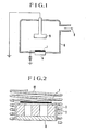
- In order to overcome such a disadvantage in the prior art sputtering apparatus, magnetron sputtering apparatus has been developed in which films can be formed more rapidly without any rise of temperature in substrates. The developed apparatus comprises an electrode and magnetic pole which are arranged so as to intersect the electric field with the magnetic field in a sputter chamber in such a manner that they are perpendicular to each other, as shown in Fig. 1. In this figure, A is a magnet system while B is an exhaust system. In this magnetron sputtering apparatus, for instance, as shown in Fig. 13, the magnetic field on an imaginary perpendicular line passing to a target through or by the magnetic symmetry axis is entirely directed to either of the target or substrate.
- However, according to said apparatus, defects with respect to structure such as micro-crack, crack and others are often happens on the surface of the formed films. Among these defects, the crack is serious in that it increases as films are increased in thickness and that cracks remarkably appear on films where substrates are made of a polymer subject to heat-deformation, such as acrylonitrile-butadiene-styrene resin. Cracks are undesirable, particularly, if films are formed for various purposes such as magnetic recording, decoration, resist, surface hardening and others. Cracks, for example, generated on the magnetic recording layer of a magnetic recording medium lead to troubles, that is, (1) reduction of recording signals; (2) frictional wear of the magnetic head according to sliding at a time of recording or playback; and (3) the reduced durability of the magnetic recording medium itself. In addition, where a vertical type magnetic recording medium is formed with a magnetic recording layer of ferromagnetic Co-Cr alloy film, etc. by the use of the prior art magnetron sputtering apparatus, a new and important problem is caused in that the coercive force perpendicular to the surface of the magnetic recording film is reduced to decrease the output on reproducing.
- In order to overcome such a disadvantage, it is effective to increase the substrate in temperature even in magnetron sputtering apparatuses. Such a procedure, however, cannot be applied to polymers subject to heat-deformation as in the planar diode sputtering apparatus, and also does not provide a desired means for preventing any crack since the magnetron sputtering apparatus constructed according to this principle becomes more complicated.
- The present invention overcomes the above-mentioned disadvantages in the prior art magnetron sputtering apparatus. An object of the present invention is to provide a magnetron sputtering apparatus which can form a metal film having no crack without heating of a substrate used therein and which can form a magnetic recording layer having an increased coercive force perpendicular to the surface of the film when it is used for formation of the film made of Co-Cr alloy.
- The present invention provides a magnetron sputtering apparatus comprising a sputtering chamber; a substrate and target disposed within said sputtering chamber to form a desired space therebetween; means for applying a voltage between said substrate and target; and means for producing a magnetic field; said apparatus being characterised in that said magnetic field-producing means is adapted to excite a magnetic field so that the direction of the magnetic field may be inverted on the magnetic symmetry axis within said space.
- The other objects and advantages of the present invention will be apparent from reading the following detailed description in connection with the accompanying drawings in which:
- Fig. 1 is a schematic view of the prior art magnetron sputtering apparatus;
- Fig. 2 is a diagrammatic side view of a magnetic field-producing means which consists of a permanent magnet and a solenoid coil in combination;
- Fig. 3 is a diagrammatic plan view of a magnetic field-producing means according to the present invention;
- Fig. 4 is a longitudinal section view taken along a line IV - IV in Fig. 3;
- Fig. 5 is a diagrammatic view illustrating the direction of a magnetic field which is produced between a target and substrate in Example 1;
- Fig. 6 is a view showing a curve with respect to the relationship between the height from the target surface and the intensity of vertical component in the magnetic field in Example 1;
- Fig. 7 is a longitudinal section of another magnetic field-producing means constructed in accordance with the present invention;
- Fig. 8 is a view showing a curve with respect to the relationship between the height from the target surface and the intensity of vertical component in the magnetic field in Example 2;
- Fig. 9 is a schematic view of a film carrying system;
- Fig. 10 is a schematic view showing another example of the film carrying system;
- Fig. 11 is a diagrammatic plan view of the prior art magnetic field-producing means;
- Fig. 12 is a longitudinal section taken along a line XII - XII in Fig. 11;
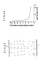
- Fig. 13 is a diagrammatic view illustrating the direction of a magnetic field which is produced between a target and substrate in Comparative example 1;
- Fig. 14 is a view showing a curve with respect to the relationship between the height from the target surface and the intensity of vertical component in the magnetic field in Comparative example 1;
- Fig. 15 is a longitudinal section of the other magnetic field-producing means in the prior art; and
- Fig. 16 is a view showing a curve with respect to the relationship between the height from the target surface and the intensity of vertical component in the magnetic field in Comparative example 2.
- The magnetron sputtering apparatus according to the present invention comprises main components of a sputtering chamber, a target and substrate disposed within said chamber, a source of electric power for providing an electric field between the target and substrate, and means for producing a magnetic field. More particularly, an electric field is formed by a voltage which is applied between the target and the substrate, for example, by energizing a target electrode disposed on the back of the target and an electrode (substrate holder) disposed on the back of the substrate. Further, a magnetic field is formed between the target and substrate, for example, by a magnetic field-producing means located on the back of the target such that part of the magnetic field will intersect the above electric field at right angle.
- The magnetic field-producing means used in the present invention includes a permanent magnet, solenoid coil and the like which may be disposed to form the above-mentioned magnetic field. Alternatively, the magnetic field-producing means may include various combinations, that is, a combination of permanent magnets with a solenoid coil, a combination of permanent magnets with a yoke made of a ferromagnetic material being relatively soft in its magnetic property such as iron, etc., and a combination of permanent magnets with the yoke and solenoid coil. In these means, the combination of the permanent magnets with the yoke and the combination of the permanent magnets with the yoke and solenoid coil are preferred.
- Some embodiments of magnetic field-producing means according to the present invention will now be described.
- If it is desired to form the above-mentioned magnetic field only by the use of permanent magnets, one of the permanent magnets (A sectional area parallel to the target surface is referred to 51. The permanent magnet will be abbreviated to magnet I for convenience sake.) is located on the central area of the back of a target with the south pole of the magnet being faced to the target. A plurality of additional magnets (The total sectional area parallel to the surface of the target is referred to S2. The additional magnets will be abbreviated to magnets II for convenience sake.) having substantially the same function as the above magnet I are disposed on the back of the target along the peripheral edge thereof symmetrically about the magnet I with the north poles thereof being faced to the target. At this time, the sectional area S2 should be enough larger than the
sectional area 51. Preferably, the ratio of S2 to S1 is three or more. Thus, the magnet I is magnetically saturated while the magnetic flux from the north poles of the magnets II penetrates in part into the south pole of the magnet I and directly returns in part to the south poles of the magnets II themselves. Accordingly, the magnetic field produced by the magnets I and II will be inverted in direction on the magnetic symmetry axis. - Further, the magnetic poles in the magnets I and II may be reversed in direction. In such a case, the direction of the produced magnetic field will be oriented along an imaginary perpendicular line from the substrate to the target. However, the advantage of the present invention will not be adversely affected by such an orientation in the magnetic field only for such a reason why the electrons are reversed in the direction of magnetron motion. Where permanent magnets and solenoid coils are together utilized, for instance, as shown in Fig. 2, permanent magnets are disposed on the back of the
target 1 as in the arrangement in which only a permanent magnets are used described hereinbefore in addition to an arrangement in which atarget 1 andsolenoid coil 12 are located. By using the solenoid coils, the distribution of magnetic field can be controlled simply by changing the current passing through the solenoid coils. - Where permanent magnets are used in combination with a yoke, the permanent magnets are arranged in a manner similar to that in the aforementioned structure in which only the permanent magnets are used, except that the yoke is made of a ferromagnetic material being relatively soft in its magnetic property and located on the central area of the back of the target (see Figs. 3 and 4). In consideration with the differential saturated magnetic flux between the yoke and permanent magnets and the magnetic property of the yoke, such a structure provides the desired magnetic field on the basis of the similar saturation magnetization phenomenone and the flow of flux created by the magnetic resistance in the yoke.
- Further, even in such an arrangement that the magnet-yoke system shown in Figs. 3 and 4 is combined with solenoid coils arranged as shown in Fig. 2, magnetic field-producing means capable of controlling the magnetic field can be provided.
- The magnetron sputtering apparatus of the present invention may be used to form a plurality of magnetic fields with respect to the present invention in the same target.
- The magnetron sputtering apparatus including the aforementioned magnetic field-producing means can continuously operate sputtering by moving the substrate without interruption (Fig. 9).
- If such an apparatus as shown in Fig. 10 is used, the substrate can be sputtered at its opposite faces. In practice, the magnetron sputtering apparatus of Fig. 10 is preferably used to manufacture, for example, a floppy disc having magnetic recording media which are formed on its opposite faces.
- By using the magnetron sputtering apparatus provided as described hereinbefore, a magnetic field may be improved in comparison with the prior art sputtering apparatuses. As a result, charged particles (for example, electrons) may properly be incident upon the substrate to increase only the surface of the substrate in temperature without any crack.
- In accordance with the present invention, the magnetron sputtering apparatus can form metal films having no crack without heating of the substrate and also form a magnetic recording layer having an increased coercive force perpendicular to the surface of the film when applied it to the formation of the film made of Co-Cr alloy.
- Some examples and comparative examples will be described hereinbelow.
- As shown in Figs. 3 and 4, a
target 1 of 60 mm x 120 mm was located on the upper face of acopper electrode 2. Samarium -cobalt magnets 3 of 15.2 mm diameter and 20 mm height were disposed as shown by broken lines in Fig. 3 with the north poles thereof being faced to the underside of thetarget 1. Substantially E-shaped yoke 4 was disposed below the undersides of the magnets and also at the central area of the underside of thetarget electrode 2. The direction of the magnetic field produced in the space above thetarget 1 and the intensity of the vertical component in this magnetic fiels (oersted Oe) are shown in Figs. 5 and 6, respectively. Fig. 5 is a diagrammatic view in which the direction of the magnetic field between thetarget 1 and thesubstrate 5 is shown by arrows. Fig. 6 illustrates the intensity of vertical components in the magnetic field on an imaginary perpendicular passing through or by the center of the magnetic circuit in the space above thetarget 1 toward thetarget 1. In Fig. 6, the vertical line represents the intensity as plus in the direction of target while the horizontal line represents the height from the target surface (mm). - In the above-mentioned magnetron sputtering apparatus, the spacing between the
target 1 and thesubstrate 5 was 100 mm, and the substrate was made of acrylonitrile-butadiene-styrene resin. The sputteringchamber 6 was filled with argon gas of 5 x 10⁻³ Torr. Thereafter, 0 films were formed at sputtering speeds of 600 A/min. and 0 1000 A/min. without heating. - The
target 1 was made of three different materials, that is, chromium (Cr) with 1.0 mm thickness, cobalt (Co) - chromium (Cr) alloy with 2.0 mm thickness and its saturation magnetization of 450 gausses, and iron (Fe) - nickel (Ni) alloy with 2.0 mm thickness and its saturation magnetization of 620 gausses. By using the respective targets made of these materials, films of 1000 Å, 5000 Å and 5000 Å thickness were obtained, respectively. - With visual and microscopic observations, no crack could be found on all the films obtained. In any event, the Co-Cr alloy film was 1080 oersteds in its coercive forces perpendicular to the surface thereof.
- As shown in Fig. 7, a
target 1 of 60 mm diameter was used while a magnet 3' of 23.6 mm diameter slightly larger than that of the magnet in Example 1 was located with the south pole thereof being faced to the central area of the underside of atarget electrode 2. Further, thesame magnets 3 as in Example 1 were disposed about thetarget magnet 2 along the peripheral edge of the underside of the target electrode with the north poles thereof being faced to the underside of the target electrode. Films were made through the same procedure as in Example 1. Ratio of S2/S1 was approximately 5. The direction of magnetic field was substantially identical with that of Fig. 5. Fig. 8 shows a curve with respect to the relationship between the height from the surface of thetarget 1 and the intensity of vertical components in the magnetic field. - Three
different targets 1 were made respectively of chromium with 1.0 mm thickness, Co-Cr alloy with 3.5 mm thickness and its saturation magnetization of 350 gausses, and Fe-Ni alloy with 2.5 mm thickness and its saturation magnetization of 620 gausses. Films obtained by using these targets had no crack. Co-Cr alloy film was 1120 oersteds in its coercive force perpendicular to the surface thereof. - The apparatus used in Example 1 was combined with a film carrying system shown in Fig. 9 in which the
substrate 5 was moved in the direction shown by an arrow. Thus, there was provided a magnetron sputtering apparatus for continuously forming films. - The film carrying system included a supply roll 7 around which an elongated film-shaped
substrate 5 is wound; guiderollers 8 for guiding thesubstrate 5 continuously fed to a sputtering station; asubstrate holder 9 spaced from and opposed to atarget 1 by a distance of 100 mm with the underside thereof slidably engaging with the movingsubstrate 5; a take-up roll 10 around which the treatedsubstrate 5 is rolled; and amask 11 spaced away from thesubstrate 5 by 0.5 mm to provide a sputtering region having its longitudinal dimension of 70 mm for thesubstrate 5. - In the above apparatus, the
substrate 5 was Kapton film (trade name, available from Du Pont de Nemours & Co. Inc.) of 25 pm thickness and 1/2 inches width while thetarget 1 was made of Co-Cr alloy with the dimensions of 60 mm x 120 mm x 2.0 mm and itssaturation magnetization 0 of 450 gausses. Films of 2400 A thickness were formed as the substrate was moved at speeds of 0.93 cm/min. and 1.9 cm/min. - The resulting films had no crack. The coercive force perpendicular to the surface of film was 930 oersteds at the substrate moving speed of 0.93 cm/min. and 1050 oersteds at the substrate moving speed of 1.9 cm/min.
- A magnetron sputtering apparatus was composed of the apparatus used in Example 2 and the film carrying system used in Example 3.
- The sputtering region had its dimension of 30 mm. The
target 1 was made of Co-Cr alloy with a diameter of 60 mm and a thickness of 3.7 mm and with its saturation magnetization of 350 gausses. The substrate was moved at two speeds of 0.3 cm/min. and 0.4 cm/min. Films having a 0 thickness of 2400 A were formed through the same pocedure as in Example 3. - The resulting films had no crack. The coercive force perpendicular to the surface of film was 1350 oersteds at the substrate moving speed of 0.3 cm/min. and 1400 oersteds at 0.4 cm/min.
- As shown in Figs. 11 and 12, samarium-
cobalt magnet 3 having dimensions of 18 mm x 78 mm x 15.5 mm (height) was located below the central area of acopper target electrode 2 with the south pole of themagnet 3 being faced to the underside of theelectrode 2. A yoke 4 of iron was disposed below the magnet with the peripheral upstanding portion of the yoke opposed to the peripheral undeside portion of thetarget electrode 2. Films were formed through the same procedure as in Example 1 without heating of the substrate. Fig. 13 shows the direction of the magnetic field produced in this example while Fig. 14 shows a curve representing the relationship between the height from the surface of thetarget 1 and the intensity of vertical components in the magnetic field. - The magnetic field was identical with that of the prior art sputtering apparatus. The direction of magnetic field on an imaginary perpendicular line passing through or by the center of the magnetic circuit toward the
target 1 was fully oriented to the target. - All the resulting films had remarkable cracks. The same results were obtained even if the spacing between the target and the substrate was selected both to be 50 mm and 150 mm. The coercive force perpendicular to the surface of the Co-Cr alloy film was 380 oersteds.
- As shown in Fig. 15, a samarium-
cobalt magnet 3 having a diameter of 20 mm and a height of 20 mm was located below atarget electrode 2 at the central underside thereof. A plurality of similar samarium-cobalt magnets 3 of 10 mm x 20 mm x 2.5 mm were disposed below thetarget electrode 2 along the peripheral underside thereof. Films were formed through the same procedure as in Example 2. A curve representing the relationship between the height from the surface of thetarget 1 and the intensity of vertical components in the magnetic field in this example is shown in Fig. 16. The direction of magnetic field in the space above thetarget 1 is omitted because it is substantially identical with that of Comparative example 1. - All the resulting films had remarklable cracks. The same results were obtained even if the spacing between the target and substrate was changed to 50 mm; the speed at o whcih the films were formed to 300 A/min.; the pressure of argon gas to 2.8 x 10⁻³ Torr and 7 x 10⁻³ Torr, respectively. The coercive force perpendicular to the surface of the Co-Cr alloy film was 400 oersteds.
- By using a magnetron sputtering apparatus constituted of the apparatus used in Comparative example 1 and the film carrying system of Example 3 incorporated into the above apparatus, films were formed through the same procedure as in Example 3.
- All the resulting films had remarkable cracks. The same results were obtained even though the spacing between the target and substrate was changed to 50 mm and 120 mm; and the pressure of argon gas to 3 x 10⁻³ Torr and 6.5 x 10⁻³ Torr, respectively. The coercive force perpendicular to the surface of the film was 420 oersteds at the substrate moving speed of 0.93 cm/min. and 380 oersteds at 1.9 cm/min.
- A magnetron sputtering apparatus was obtained by incorporating the film carrying system of Example 3 into the apparatus of Comparative example 2. By using such an apparatus, films were obtained through the same procedure as in Example 4.
- All the resulting films had remarkable cracks. The coercive force perpendicular to the film surface was 400 oersteds at both the substrate moving speeds of 0.3 cm/min. and 0.4 cm/min.
Claims (13)
Applications Claiming Priority (2)
| Application Number | Priority Date | Filing Date | Title |
|---|---|---|---|
| JP71556/82 | 1982-04-30 | ||
| JP57071556A JPS58189372A (en) | 1982-04-30 | 1982-04-30 | Magnetron sputtering device |
Publications (2)
| Publication Number | Publication Date |
|---|---|
| EP0093412A1 true EP0093412A1 (en) | 1983-11-09 |
| EP0093412B1 EP0093412B1 (en) | 1987-04-08 |
Family
ID=13464114
Family Applications (1)
| Application Number | Title | Priority Date | Filing Date |
|---|---|---|---|
| EP83104178A Expired EP0093412B1 (en) | 1982-04-30 | 1983-04-28 | Magnetron sputtering apparatusand a method for forming a magnetic thinfilm on the surface of a substrate |
Country Status (4)
| Country | Link |
|---|---|
| US (1) | US4441974A (en) |
| EP (1) | EP0093412B1 (en) |
| JP (1) | JPS58189372A (en) |
| DE (1) | DE3370830D1 (en) |
Cited By (2)
| Publication number | Priority date | Publication date | Assignee | Title |
|---|---|---|---|---|
| GB2144772A (en) * | 1983-07-19 | 1985-03-13 | Varian Associates | Magnetron sputter coating source for both magnetic and nonmagnetic target materials |
| EP0416241A2 (en) * | 1989-09-07 | 1991-03-13 | Leybold Aktiengesellschaft | Apparatus for coating a substrate |
Families Citing this family (34)
| Publication number | Priority date | Publication date | Assignee | Title |
|---|---|---|---|---|
| US4666788A (en) * | 1982-02-16 | 1987-05-19 | Teijin Limited | Perpendicular magnetic recording medium, method for producing the same, and sputtering device |
| US4569746A (en) * | 1984-05-17 | 1986-02-11 | Varian Associates, Inc. | Magnetron sputter device using the same pole piece for coupling separate confining magnetic fields to separate targets subject to separate discharges |
| US4606806A (en) * | 1984-05-17 | 1986-08-19 | Varian Associates, Inc. | Magnetron sputter device having planar and curved targets |
| US4657654A (en) * | 1984-05-17 | 1987-04-14 | Varian Associates, Inc. | Targets for magnetron sputter device having separate confining magnetic fields to separate targets subject to separate discharges |
| US4595482A (en) * | 1984-05-17 | 1986-06-17 | Varian Associates, Inc. | Apparatus for and the method of controlling magnetron sputter device having separate confining magnetic fields to separate targets subject to separate discharges |
| US4865708A (en) * | 1988-11-14 | 1989-09-12 | Vac-Tec Systems, Inc. | Magnetron sputtering cathode |
| US4892633A (en) * | 1988-11-14 | 1990-01-09 | Vac-Tec Systems, Inc. | Magnetron sputtering cathode |
| US5130170A (en) * | 1989-06-28 | 1992-07-14 | Canon Kabushiki Kaisha | Microwave pcvd method for continuously forming a large area functional deposited film using a curved moving substrate web with microwave energy with a directivity in one direction perpendicular to the direction of microwave propagation |
| US5455197A (en) * | 1993-07-16 | 1995-10-03 | Materials Research Corporation | Control of the crystal orientation dependent properties of a film deposited on a semiconductor wafer |
| US5332637A (en) * | 1993-08-31 | 1994-07-26 | Eastman Kodak Company | Electrostatographic dry toner and developer compositions with hydroxyphthalimide |
| US5358816A (en) * | 1993-08-31 | 1994-10-25 | Eastman Kodak Company | Zinc salt of ortho-benzoic sulfimide as negative charge-controlling additive for toner and developer compositions |
| US5358815A (en) * | 1993-08-31 | 1994-10-25 | Eastman Kodak Company | Toner compositions containing negative charge-controlling additive |
| US5358817A (en) * | 1993-08-31 | 1994-10-25 | Eastman Kodak Company | Toner compositions containing as a negative charge-controlling agent the calcium salt of ortho-benzoic sulfimide |
| US5358814A (en) * | 1993-08-31 | 1994-10-25 | Eastman Kodak Company | Toner compositions containing as a negative charge-controlling agent a mixture of ortho-benzoic sulfimide and para-anisic acid |
| US5358818A (en) * | 1993-08-31 | 1994-10-25 | Eastman Kodak Company | Ortho-benzoic sulfimide as charge-controlling agent |
| SE509933C2 (en) | 1996-09-16 | 1999-03-22 | Scandinavian Solar Ab | Methods and apparatus for producing a spectrally selective absorbent layer for solar collectors and produced layer |
| US6093290A (en) * | 1997-05-14 | 2000-07-25 | Canon Kabushiki Kaisha | Method of generating a reciprocating plurality of magnetic fluxes on a target |
| US6042700A (en) * | 1997-09-15 | 2000-03-28 | Applied Materials, Inc. | Adjustment of deposition uniformity in an inductively coupled plasma source |
| JP4204978B2 (en) * | 2001-12-19 | 2009-01-07 | 日鉱金属株式会社 | Method of joining magnetic target and backing plate and magnetic target |
| US7205960B2 (en) | 2003-02-19 | 2007-04-17 | Mirage Innovations Ltd. | Chromatic planar optic display system |
| US7297422B2 (en) * | 2003-12-19 | 2007-11-20 | Seagate Technology Llc | Method for sputtering magnetic recording media |
| US7499216B2 (en) * | 2004-07-23 | 2009-03-03 | Mirage Innovations Ltd. | Wide field-of-view binocular device |
| US7492512B2 (en) * | 2004-07-23 | 2009-02-17 | Mirage International Ltd. | Wide field-of-view binocular device, system and kit |
| US7573640B2 (en) * | 2005-04-04 | 2009-08-11 | Mirage Innovations Ltd. | Multi-plane optical apparatus |
| EP1942364A1 (en) | 2005-09-14 | 2008-07-09 | Mirage Innovations Ltd. | Diffractive optical relay and method for manufacturing the same |
| EP1932051A1 (en) * | 2005-09-14 | 2008-06-18 | Mirage Innovations Ltd. | Diffraction grating with a spatially varying duty-cycle |
| US20080043334A1 (en) * | 2006-08-18 | 2008-02-21 | Mirage Innovations Ltd. | Diffractive optical relay and method for manufacturing the same |
| DE602006005177D1 (en) * | 2005-11-03 | 2009-03-26 | Mirage Innovations Ltd | BINOCULAR OPTICAL RELAY DEVICE |
| US20100177388A1 (en) * | 2006-08-23 | 2010-07-15 | Mirage Innovations Ltd. | Diffractive optical relay device with improved color uniformity |
| JP5300084B2 (en) * | 2007-06-01 | 2013-09-25 | 国立大学法人山口大学 | Thin film sputtering equipment |
| US20100302644A1 (en) * | 2007-09-18 | 2010-12-02 | Mirage Innovations Ltd | Slanted optical device |
| JP2012112040A (en) * | 2010-11-05 | 2012-06-14 | Shin-Etsu Chemical Co Ltd | Magnetic circuit for sputtering apparatus |
| JP5810427B2 (en) * | 2012-03-29 | 2015-11-11 | Shマテリアル株式会社 | Sputtering apparatus for lead frame material for mounting semiconductor light emitting element and method for manufacturing lead frame material for mounting semiconductor light emitting element |
| JP6572800B2 (en) * | 2016-02-26 | 2019-09-11 | 株式会社村田製作所 | Vacuum equipment |
Citations (5)
| Publication number | Priority date | Publication date | Assignee | Title |
|---|---|---|---|---|
| US4169031A (en) * | 1978-01-13 | 1979-09-25 | Polyohm, Inc. | Magnetron sputter cathode assembly |
| GB2028377A (en) * | 1978-08-21 | 1980-03-05 | Vac Tec Syst | Magnetically-Enhanced Sputtering Device |
| US4198283A (en) * | 1978-11-06 | 1980-04-15 | Materials Research Corporation | Magnetron sputtering target and cathode assembly |
| US4309266A (en) * | 1980-07-18 | 1982-01-05 | Murata Manufacturing Co., Ltd. | Magnetron sputtering apparatus |
| GB2078787A (en) * | 1980-06-23 | 1982-01-13 | Vac Tec Syst | Magnetron sputtering device having a plurality of magnetic field sources |
Family Cites Families (10)
| Publication number | Priority date | Publication date | Assignee | Title |
|---|---|---|---|---|
| US3878085A (en) * | 1973-07-05 | 1975-04-15 | Sloan Technology Corp | Cathode sputtering apparatus |
| US4116793A (en) * | 1974-12-23 | 1978-09-26 | Telic Corporation | Glow discharge method and apparatus |
| US4265729A (en) * | 1978-09-27 | 1981-05-05 | Vac-Tec Systems, Inc. | Magnetically enhanced sputtering device |
| US4162954A (en) * | 1978-08-21 | 1979-07-31 | Vac-Tec Systems, Inc. | Planar magnetron sputtering device |
| US4180450A (en) * | 1978-08-21 | 1979-12-25 | Vac-Tec Systems, Inc. | Planar magnetron sputtering device |
| JPS5531142A (en) * | 1978-08-25 | 1980-03-05 | Tomonobu Hata | Pressed magnetic field type magnetron sputter by focusing magnetic field |
| JPS55107776A (en) * | 1979-02-10 | 1980-08-19 | Hitachi Ltd | Planer type high speed magnetron sputtering apparatus |
| US4312731A (en) * | 1979-04-24 | 1982-01-26 | Vac-Tec Systems, Inc. | Magnetically enhanced sputtering device and method |
| US4239611A (en) * | 1979-06-11 | 1980-12-16 | Vac-Tec Systems, Inc. | Magnetron sputtering devices |
| US4361472A (en) * | 1980-09-15 | 1982-11-30 | Vac-Tec Systems, Inc. | Sputtering method and apparatus utilizing improved ion source |
-
1982
- 1982-04-30 JP JP57071556A patent/JPS58189372A/en active Granted
-
1983
- 1983-04-28 US US06/489,593 patent/US4441974A/en not_active Expired - Lifetime
- 1983-04-28 DE DE8383104178T patent/DE3370830D1/en not_active Expired
- 1983-04-28 EP EP83104178A patent/EP0093412B1/en not_active Expired
Patent Citations (5)
| Publication number | Priority date | Publication date | Assignee | Title |
|---|---|---|---|---|
| US4169031A (en) * | 1978-01-13 | 1979-09-25 | Polyohm, Inc. | Magnetron sputter cathode assembly |
| GB2028377A (en) * | 1978-08-21 | 1980-03-05 | Vac Tec Syst | Magnetically-Enhanced Sputtering Device |
| US4198283A (en) * | 1978-11-06 | 1980-04-15 | Materials Research Corporation | Magnetron sputtering target and cathode assembly |
| GB2078787A (en) * | 1980-06-23 | 1982-01-13 | Vac Tec Syst | Magnetron sputtering device having a plurality of magnetic field sources |
| US4309266A (en) * | 1980-07-18 | 1982-01-05 | Murata Manufacturing Co., Ltd. | Magnetron sputtering apparatus |
Non-Patent Citations (4)
| Title |
|---|
| IBM TECHNICAL DISCLOSURE BULLETIN, vol. 24, no. 7B, December 1981, * Pages 3632-3635, especially 3633 * * |
| PATENT ABSTRACTS OF JAPAN, unexamined applications, C field, vol. 5, no. 180, November 19, 1981 THE PATENT OFFICE JAPANESE GOVERNMENT page 126 C 79; & JP-A-56 105 474 ( MATSUSHITA DENKI SANGYO K.K. ) * |
| PATENT ABSTRACTS OF JAPAN, unexamined applications, C field, vol. 5, no. 20, February 6, 1981 THE PATENT OFFICE JAPANESE GOVERNMENT page 158 C 42; & JP-A-55 148 769 ( TOKYO SHIBAURA DENKI K. K. ) * |
| PATENT ABSTRACTS OF JAPAN, unexamined applications, C field, vol. 6, no. 11, January 22, 1982 THE PATENT OFFICE JAPANESE GOVERNMENT page 28 C 88; & JP-A-56 133 460 ( TOKYO SHIBAURA DENKI K.K. ) * |
Cited By (3)
| Publication number | Priority date | Publication date | Assignee | Title |
|---|---|---|---|---|
| GB2144772A (en) * | 1983-07-19 | 1985-03-13 | Varian Associates | Magnetron sputter coating source for both magnetic and nonmagnetic target materials |
| EP0416241A2 (en) * | 1989-09-07 | 1991-03-13 | Leybold Aktiengesellschaft | Apparatus for coating a substrate |
| EP0416241A3 (en) * | 1989-09-07 | 1991-10-16 | Leybold Aktiengesellschaft | Apparatus for coating a substrate |
Also Published As
| Publication number | Publication date |
|---|---|
| JPS58189372A (en) | 1983-11-05 |
| US4441974A (en) | 1984-04-10 |
| JPH0411625B2 (en) | 1992-03-02 |
| EP0093412B1 (en) | 1987-04-08 |
| DE3370830D1 (en) | 1987-05-14 |
Similar Documents
| Publication | Publication Date | Title |
|---|---|---|
| US4441974A (en) | Magnetron sputtering apparatus | |
| US4670356A (en) | Magneto-optical recording medium and method of making same | |
| CA1325792C (en) | Method of producing a thin film by sputtering and an opposed target type sputtering apparatus | |
| US3898952A (en) | Apparatus for production of magnetic recording medium | |
| US5403457A (en) | Method for making soft magnetic film | |
| EP0122030B1 (en) | A magnetic recording member and a manufacturing method for such a member | |
| JPS6134723A (en) | Magnetic recording medium and its manufacture | |
| JPH0454367B2 (en) | ||
| JPH039126Y2 (en) | ||
| JPS58199862A (en) | Magnetron type sputtering device | |
| US4563396A (en) | Magnetic recording medium | |
| JPS6367328B2 (en) | ||
| JP3132254B2 (en) | Soft magnetic film and method for manufacturing soft magnetic multilayer film | |
| JP2821622B2 (en) | Oblique orientation device | |
| JP2710048B2 (en) | Perpendicular magnetic recording medium and manufacturing method thereof | |
| JPS5917896Y2 (en) | Target electrode for high speed sputtering | |
| JPH02205673A (en) | Magnetron cathode structure | |
| JPH0550052B2 (en) | ||
| JPS59157828A (en) | Magnetic recording medium | |
| JPH09157843A (en) | Sputtering device | |
| JPH02187916A (en) | Perpendicular magnetic recording medium and production thereof | |
| JPS6224432A (en) | Production of magnetic recording medium | |
| JPS61104431A (en) | Production of vertical recording magnetic medium | |
| JPH02267263A (en) | Target for magnetron sputtering | |
| Takahashi et al. | Composition and Characteristics of Sputtered Co-Cr Films |
Legal Events
| Date | Code | Title | Description |
|---|---|---|---|
| PUAI | Public reference made under article 153(3) epc to a published international application that has entered the european phase |
Free format text: ORIGINAL CODE: 0009012 |
|
| AK | Designated contracting states |
Designated state(s): DE FR GB IT NL |
|
| 17P | Request for examination filed |
Effective date: 19840308 |
|
| RAP1 | Party data changed (applicant data changed or rights of an application transferred) |
Owner name: TOKUDA SEISAKUSHO, LTD. Owner name: KABUSHIKI KAISHA TOSHIBA |
|
| GRAA | (expected) grant |
Free format text: ORIGINAL CODE: 0009210 |
|
| AK | Designated contracting states |
Kind code of ref document: B1 Designated state(s): DE FR GB IT NL |
|
| PG25 | Lapsed in a contracting state [announced via postgrant information from national office to epo] |
Ref country code: IT Free format text: LAPSE BECAUSE OF FAILURE TO SUBMIT A TRANSLATION OF THE DESCRIPTION OR TO PAY THE FEE WITHIN THE PRESCRIBED TIME-LIMIT;WARNING: LAPSES OF ITALIAN PATENTS WITH EFFECTIVE DATE BEFORE 2007 MAY HAVE OCCURRED AT ANY TIME BEFORE 2007. THE CORRECT EFFECTIVE DATE MAY BE DIFFERENT FROM THE ONE RECORDED. Effective date: 19870408 |
|
| REF | Corresponds to: |
Ref document number: 3370830 Country of ref document: DE Date of ref document: 19870514 |
|
| ET | Fr: translation filed | ||
| PLBE | No opposition filed within time limit |
Free format text: ORIGINAL CODE: 0009261 |
|
| STAA | Information on the status of an ep patent application or granted ep patent |
Free format text: STATUS: NO OPPOSITION FILED WITHIN TIME LIMIT |
|
| 26N | No opposition filed | ||
| REG | Reference to a national code |
Ref country code: GB Ref legal event code: 732E |
|
| REG | Reference to a national code |
Ref country code: FR Ref legal event code: TP |
|
| NLS | Nl: assignments of ep-patents |
Owner name: KABUSHIKI KAISHA TOSHIBA TE KAWASAKI EN SHIBAURA E |
|
| REG | Reference to a national code |
Ref country code: GB Ref legal event code: IF02 |
|
| PGFP | Annual fee paid to national office [announced via postgrant information from national office to epo] |
Ref country code: GB Payment date: 20020416 Year of fee payment: 20 |
|
| PGFP | Annual fee paid to national office [announced via postgrant information from national office to epo] |
Ref country code: FR Payment date: 20020417 Year of fee payment: 20 |
|
| PGFP | Annual fee paid to national office [announced via postgrant information from national office to epo] |
Ref country code: NL Payment date: 20020430 Year of fee payment: 20 Ref country code: DE Payment date: 20020430 Year of fee payment: 20 |
|
| PG25 | Lapsed in a contracting state [announced via postgrant information from national office to epo] |
Ref country code: GB Free format text: LAPSE BECAUSE OF EXPIRATION OF PROTECTION Effective date: 20030427 |
|
| PG25 | Lapsed in a contracting state [announced via postgrant information from national office to epo] |
Ref country code: NL Free format text: LAPSE BECAUSE OF EXPIRATION OF PROTECTION Effective date: 20030428 |
|
| REG | Reference to a national code |
Ref country code: GB Ref legal event code: PE20 |
|
| NLV7 | Nl: ceased due to reaching the maximum lifetime of a patent |
Effective date: 20030428 |