EP0093086A2 - Bipolare Halbleiteranordnung und MOS-Schaltung mit solch einer Anordnung - Google Patents
Bipolare Halbleiteranordnung und MOS-Schaltung mit solch einer Anordnung Download PDFInfo
- Publication number
- EP0093086A2 EP0093086A2 EP83810169A EP83810169A EP0093086A2 EP 0093086 A2 EP0093086 A2 EP 0093086A2 EP 83810169 A EP83810169 A EP 83810169A EP 83810169 A EP83810169 A EP 83810169A EP 0093086 A2 EP0093086 A2 EP 0093086A2
- Authority
- EP
- European Patent Office
- Prior art keywords
- type
- conductivity
- region
- substrate
- transistor
- Prior art date
- Legal status (The legal status is an assumption and is not a legal conclusion. Google has not performed a legal analysis and makes no representation as to the accuracy of the status listed.)
- Withdrawn
Links
Images


Classifications
-
- H—ELECTRICITY
- H03—ELECTRONIC CIRCUITRY
- H03F—AMPLIFIERS
- H03F3/00—Amplifiers with only discharge tubes or only semiconductor devices as amplifying elements
- H03F3/34—DC amplifiers in which all stages are DC-coupled
- H03F3/343—DC amplifiers in which all stages are DC-coupled with semiconductor devices only
- H03F3/345—DC amplifiers in which all stages are DC-coupled with semiconductor devices only with field-effect devices
-
- G—PHYSICS
- G05—CONTROLLING; REGULATING
- G05F—SYSTEMS FOR REGULATING ELECTRIC OR MAGNETIC VARIABLES
- G05F3/00—Non-retroactive systems for regulating electric variables by using an uncontrolled element, or an uncontrolled combination of elements, such element or such combination having self-regulating properties
- G05F3/02—Regulating voltage or current
- G05F3/08—Regulating voltage or current wherein the variable is DC
- G05F3/10—Regulating voltage or current wherein the variable is DC using uncontrolled devices with non-linear characteristics
- G05F3/16—Regulating voltage or current wherein the variable is DC using uncontrolled devices with non-linear characteristics being semiconductor devices
- G05F3/20—Regulating voltage or current wherein the variable is DC using uncontrolled devices with non-linear characteristics being semiconductor devices using diode- transistor combinations
- G05F3/26—Current mirrors
- G05F3/267—Current mirrors using both bipolar and field-effect technology
-
- H—ELECTRICITY
- H10—SEMICONDUCTOR DEVICES; ELECTRIC SOLID-STATE DEVICES NOT OTHERWISE PROVIDED FOR
- H10D—INORGANIC ELECTRIC SEMICONDUCTOR DEVICES
- H10D84/00—Integrated devices formed in or on semiconductor substrates that comprise only semiconducting layers, e.g. on Si wafers or on GaAs-on-Si wafers
- H10D84/40—Integrated devices formed in or on semiconductor substrates that comprise only semiconducting layers, e.g. on Si wafers or on GaAs-on-Si wafers characterised by the integration of at least one component covered by groups H10D12/00 or H10D30/00 with at least one component covered by groups H10D10/00 or H10D18/00, e.g. integration of IGFETs with BJTs
- H10D84/401—Combinations of FETs or IGBTs with BJTs
- H10D84/403—Combinations of FETs or IGBTs with BJTs and with one or more of diodes, resistors or capacitors
- H10D84/409—Combinations of FETs or IGBTs with lateral BJTs and with one or more of diodes, resistors or capacitors
Definitions
- the present invention relates to a semiconductor device achievable in MOS technology and relates more particularly to such a device having an operating characteristic of a bipolar transistor as well as to MOS circuits incorporating MOS transistors associated with said device with bipolar operating characteristic. .
- FIG. 1 A device, as described in the above-mentioned reviews and often called “substrate MOS transistor", is represented in FIG. 1.
- an n-type substrate 1 is made of a p-type casing 2.
- a n + diffusion zone 4, in the box, is connected to an electrode E serving as an emitter while the box 2 is connected to a base electrode B and the substrate to a collector electrode C.
- the bipolar transistor thus formed has, by definition, its collector C at the potential of the substrate and the latter is connected to the positive voltage of the power source. It is understood that the applications of such a device are limited.
- an object of the present invention is a semiconductor device achievable using standard MOS technology and having the characteristics of a bipolar transistor without having the limitations of known devices.
- Another object of the invention is an integrated circuit achievable using standard MOS technology and comprising MOS transistors associated with devices having the characteristics of a bipolar transistor.
- the semiconductor device capable of being produced using MOS technology and having a bipolar transistor behavior, present on the surface of a semiconductor material of a given type of conductivity, at least a first and a second region of opposite conductivity types; said first and second regions being separated from each other by an area of said semiconductor material which is covered by a conductive grid, itself insulated from said semiconductor material by an insulating layer, and a third region of the same type of conductivity as said semiconductor material, said first, second and third regions being connected respectively to an emitter electrode, a collector electrode and a base electrode; and is characterized in that said grid is polarized so as to prevent any inversion of the type of surface conductivity of said zone and in that the junction, formed by said first region and said semiconductor material, is polarized in the direct direction, the device thus formed and polarized offering the operating characteristics of a bipolar transistor.
- Figure 2.a shows the device of the invention, achievable using standard MOS technology and having characteristics of bipolar transistor when it is suitably polarized.
- a p-type box 11 In an n-type substrate 10 is produced, for example by means of a diffusion, a p-type box 11. The box 11 is connected, via a p-type diffusion, to a base electrode B, while two n-type diffusions are connected one 14 to an emitter electrode E and the other 13 to a collector electrode C.
- a grid 16, made of metal or of doped polycrystalline silicon, is deposited on an insulating oxide 15 above the space between the two diffusions 13 and 14; it is connected to a gate electrode G.
- the substrate 10 is connected to an electrode S via a diffusion 17 of n + type .
- the structure of the invention differs from that of the prior art (FIG. 1) by the presence of a gate 16.
- the gate electrode G is brought to a sufficiently negative potential, to avoid the inversion of the conductivity type of the area between the diffusions 13 and 14, and the pn junction, box 11-substrate 10, is polarized in the opposite direction.
- the junction of emitter n + - p is polarized in the direct direction, electrons are emitted in the chamber 11 (connected to the base electrode B), a part of which is collected by the collector C (the collector junction n + - p being reverse biased).
- FIG. 2.b represents the variations of the collector current I C as a function of the potential applied to the emitter E for different values of the gate voltage V G. All the potentials being defined relative to the box 11, the collector is maintained at a fixed voltage of 2 volts and the electrode S is subjected to a positive voltage so as to block the junction box-substrate.
- the device behaves like a MOS transistor.
- the same law of variation is obtained for negative values of the emitter potential.
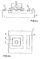
- FIGS. 3.a and 3.b show a variant of the previous device in which the manifold diffusion 13 completely surrounds the emitter diffusion 14.
- FIG. 3.b shows the arrangement of the grid 16 and of the diffusions 12, 13 and 14 made in the box 11.
- Such an arrangement makes it possible to advantage the lateral bipolar transistor to the detriment of the transistor to the substrate and to obtain typical values of the gain in current ⁇ of the order of 50 with an emitter current 1E of 1 ⁇ A.
- Bipolar structures offer the advantage, in addition to an exponential characteristic of the emitter current as a function of the emitter-base voltage, of better matching, better reproducibility and a lower noise component at low frequency than MOS structures.
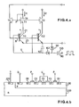
- Figure 4.a shows a current mirror where I1 is the input current and 12 the output current.
- the transistors T0, T1 and T2 are n-channel MOS transistors while Q1 and Q2 are bipolar transistors according to the invention, the symbol used being represented in FIG. 2.c.
- the MOS transistor TO supplies the basic current of the transistors Q1 and Q2. These are each connected in series with a MOS transistor, ie T1 and T2 in series with Q1 and Q2 respectively.
- the transmitters of Q1 and Q2 are connected to the negative terminal of the power source.
- the TO drain and the substrate in which the circuit is made are connected to the positive terminal of the power source.
- the gates of Q1 and Q2 are negatively polarized with respect to the transmitter thanks to the "clamping" circuit constituted by the diodes 101 and 102 and the capacitors 100 and 103 and supplied by a square signal applied to the terminal 110. If the transistors T1 and T2 on the one hand, Q1 and Q2 on the other share, are identical the output current 12 is equal to the input current 11.
- Figure 4.b shows the possible implantation of transistors T1 and Q1 of the circuit of figure 4.a.
- the n-type substrate 200 is connected to the positive terminal of the power supply via an n + type diffusion.
- the transistor Q1 is produced with a concentric structure as is the transistor T1.
- the box serves as the base electrode for transistor Q1.
- the transistors T2 and Q2, as well as other pairs of transistors Ti and Qi, can be produced in the same way in the box 210.
- the symmetry measured, namely the equality of the currents 11 and 12, of such a current mirror is four to five times better than that of an equivalent circuit working with the same input current I1 and using only MOS transistors.
- FIG. 5 shows another current mirror in which the bipolar transistors are produced directly in the n-type substrate; these bipolar transistors being of the pnp type.
- the gate electrodes G of Q3 and Q4 are brought to a more positive potential than that of the substrate (base of Q3 and Q4) either using a source external to the circuit, or by using a similar "clamping" circuit. to that of figure 4.a.
- This potential applied in G is used to produce a current I R through the resistance R.
- This current I R is equal to the sum of the current I 3 , produced by T3 and T4, and the emitter currents of Q3 and Q4. If a voltage U 1 is applied between the collector of Q3 and the negative supply terminal of the circuit and if the transistors Q3 and Q4 are identical, one obtains on the collector of Q4 an output current 12 equal to the collector current I1 of Q3.
- Figure 6 shows a circuit, which can serve as a current source, which takes advantage of the good pairing and the exponential characteristic of the bipolar transistors.
- the collector currents I1 and 12 of the transistors Q5 and Q6 respectively are linked by the relation where K 'is the ratio of the surfaces of Q6 and Q5, V is equal to R.
- I1 and U T is the thermodynamic voltage . If the transistors T5 and T6 are identical, the mirror they form imposes which results in ln K '.
- the transistor Q7 makes it possible to extract a current 13 proportional to 12.
- the gates G of the bipolar transistors Q5 to Q7 are biased by a voltage more negative than the emitter voltage and the substrate is brought to the most positive potential of the circuit.
- FIG. 7 shows a variant of the circuit of FIG. 6, capable of supplying a reference voltage V R independent of the temperature.
- V1 U T .ln K ", in which K" represents the ratio of the surfaces of the bipolar transistors Q9 and Q8.
- U T .ln K " + V BE in which VBE is the base-emitter voltage of Q8.
- This voltage V BE is a linearly decreasing function of the absolute temperature. It is therefore possible, by a judicious choice of the value of the ratio R 2 / R 1 , to make the voltage V R independent of the temperature.
- FIG. 8 shows a diagram of a differential amplifier taking advantage of the low noise and the good pairing of the bipolar transistors according to the invention.
- the block diagram of this amplifier is well known.
- the two bipolar transistors Q10 and Q11 are polarized by the current mirror formed by the MOS transistors T11 and T12 and supplied by a bias current 10.
- the two MOS transistors T9 and T10 also arranged in current mirror, constitute a load for transistors Q10 and Q11. If the potential of the inputs E and E - of the differential amplifier is sufficiently high, the gate G of the transistors Q10 and Q11 can be connected directly to the negative supply terminal of the circuit, which eliminates the need for a source d additional food.
- the SO terminal constitutes the output of this differential amplifier.
Landscapes
- Engineering & Computer Science (AREA)
- Physics & Mathematics (AREA)
- Radar, Positioning & Navigation (AREA)
- Nonlinear Science (AREA)
- Electromagnetism (AREA)
- General Physics & Mathematics (AREA)
- Microelectronics & Electronic Packaging (AREA)
- Automation & Control Theory (AREA)
- Power Engineering (AREA)
- Bipolar Transistors (AREA)
- Metal-Oxide And Bipolar Metal-Oxide Semiconductor Integrated Circuits (AREA)
- Semiconductor Integrated Circuits (AREA)
- Bipolar Integrated Circuits (AREA)
Applications Claiming Priority (2)
| Application Number | Priority Date | Filing Date | Title |
|---|---|---|---|
| CH2474/82A CH648434A5 (fr) | 1982-04-23 | 1982-04-23 | Dispositif semiconducteur presentant une caracteristique de fonctionnement d'un transistor bipolaire et circuit m0s incorporant un tel dispositif. |
| CH2474/82 | 1982-04-23 |
Publications (2)
| Publication Number | Publication Date |
|---|---|
| EP0093086A2 true EP0093086A2 (de) | 1983-11-02 |
| EP0093086A3 EP0093086A3 (de) | 1985-10-02 |
Family
ID=4234614
Family Applications (1)
| Application Number | Title | Priority Date | Filing Date |
|---|---|---|---|
| EP83810169A Withdrawn EP0093086A3 (de) | 1982-04-23 | 1983-04-22 | Bipolare Halbleiteranordnung und MOS-Schaltung mit solch einer Anordnung |
Country Status (4)
| Country | Link |
|---|---|
| EP (1) | EP0093086A3 (de) |
| JP (1) | JPS58207672A (de) |
| CA (1) | CA1245372A (de) |
| CH (1) | CH648434A5 (de) |
Cited By (6)
| Publication number | Priority date | Publication date | Assignee | Title |
|---|---|---|---|---|
| WO1986004196A1 (en) * | 1984-12-29 | 1986-07-17 | Licencia Találmányokat Értékesito^" És Innovációs | Active circuit element |
| EP0188401A3 (en) * | 1985-01-17 | 1986-09-10 | Centre Electronique Horloger S.A. | Reference voltage source |
| US4965872A (en) * | 1988-09-26 | 1990-10-23 | Vasudev Prahalad K | MOS-enhanced, self-aligned lateral bipolar transistor made of a semiconductor on an insulator |
| EP0351634A3 (de) * | 1988-07-20 | 1991-02-27 | TEMIC TELEFUNKEN microelectronic GmbH | Halbleiterschaltung für schnelle Schaltvorgänge |
| EP0700090A1 (de) * | 1994-08-19 | 1996-03-06 | Kabushiki Kaisha Toshiba | Integrierte Halbleiterschaltung mit einer Stromspiegelschaltung |
| US7217609B2 (en) | 2002-02-13 | 2007-05-15 | Infineon Technologies Ag | Semiconductor fabrication process, lateral PNP transistor, and integrated circuit |
Family Cites Families (7)
| Publication number | Priority date | Publication date | Assignee | Title |
|---|---|---|---|---|
| JPS5320872B1 (de) * | 1967-11-30 | 1978-06-29 | ||
| GB1252362A (de) * | 1969-03-11 | 1971-11-03 | ||
| US3958267A (en) * | 1973-05-07 | 1976-05-18 | National Semiconductor Corporation | Current scaling in lateral pnp structures |
| JPS50158285A (de) * | 1974-06-10 | 1975-12-22 | ||
| JPS5268382A (en) * | 1975-12-05 | 1977-06-07 | Hitachi Ltd | Semiconductor circuit unit |
| JPS52105783A (en) * | 1976-03-03 | 1977-09-05 | Hitachi Ltd | Semicondcutor unit |
| JPS5588372A (en) * | 1978-12-26 | 1980-07-04 | Sanyo Electric Co Ltd | Lateral type transistor |
-
1982
- 1982-04-23 CH CH2474/82A patent/CH648434A5/fr not_active IP Right Cessation
-
1983
- 1983-04-22 EP EP83810169A patent/EP0093086A3/de not_active Withdrawn
- 1983-04-22 JP JP58070175A patent/JPS58207672A/ja active Pending
- 1983-04-22 CA CA000426527A patent/CA1245372A/fr not_active Expired
Cited By (9)
| Publication number | Priority date | Publication date | Assignee | Title |
|---|---|---|---|---|
| WO1986004196A1 (en) * | 1984-12-29 | 1986-07-17 | Licencia Találmányokat Értékesito^" És Innovációs | Active circuit element |
| EP0188401A3 (en) * | 1985-01-17 | 1986-09-10 | Centre Electronique Horloger S.A. | Reference voltage source |
| US4672304A (en) * | 1985-01-17 | 1987-06-09 | Centre Electronique Horloger S.A. | Reference voltage source |
| EP0351634A3 (de) * | 1988-07-20 | 1991-02-27 | TEMIC TELEFUNKEN microelectronic GmbH | Halbleiterschaltung für schnelle Schaltvorgänge |
| US5036233A (en) * | 1988-07-20 | 1991-07-30 | Telefunken Electronic Gmbh | Integrated semiconductor circuit having a unidirectional semiconductor component for preventing saturation of bipolar transistors |
| US4965872A (en) * | 1988-09-26 | 1990-10-23 | Vasudev Prahalad K | MOS-enhanced, self-aligned lateral bipolar transistor made of a semiconductor on an insulator |
| EP0700090A1 (de) * | 1994-08-19 | 1996-03-06 | Kabushiki Kaisha Toshiba | Integrierte Halbleiterschaltung mit einer Stromspiegelschaltung |
| US5834814A (en) * | 1994-08-19 | 1998-11-10 | Kabushiki Kaisha Toshiba | Semiconductor integrated circuit |
| US7217609B2 (en) | 2002-02-13 | 2007-05-15 | Infineon Technologies Ag | Semiconductor fabrication process, lateral PNP transistor, and integrated circuit |
Also Published As
| Publication number | Publication date |
|---|---|
| JPS58207672A (ja) | 1983-12-03 |
| CA1245372A (fr) | 1988-11-22 |
| EP0093086A3 (de) | 1985-10-02 |
| CH648434A5 (fr) | 1985-03-15 |
Similar Documents
| Publication | Publication Date | Title |
|---|---|---|
| US4041522A (en) | Integrated circuit and manufacture thereof | |
| EP0040125B1 (de) | Schutzvorrichtung gegen Leckströme in integrierten Schaltungen | |
| FR2636778A1 (fr) | Transistor mos composite et application a une diode roue libre | |
| EP0380168A1 (de) | Integrierte Halbleitervorrichtung, die einen Feldeffekt-Transistor mit isoliertem, auf einem erhöhtem Pegel vorgespanntem Gate enthält | |
| FR2490874A1 (fr) | Transistors du type a grille isolee | |
| EP0006474A1 (de) | Verfahren zur Korrektur des Spannungskoeffizienten von ionenimplantierten oder diffundierten Halbleiterwiderständen | |
| EP0432058A1 (de) | Dynamische Isolierschaltung für integrierte Schaltungen | |
| EP0614232B1 (de) | Referenzdiode in integriertem Bipolarschaltkreis | |
| EP0543745B1 (de) | MOS-Transistor mit integrierter Zener-Schutzdiode | |
| EP0305253B1 (de) | Mikrowellentransistor mit Doppelheteroübergang | |
| EP1231642A1 (de) | Photodetektor mit drei Transistoren | |
| FR3003996A1 (fr) | Procede de commande d'un circuit integre | |
| FR2507819A1 (fr) | Dispositif de protection contre les surcharges pour circuit integre et circuit integre de protection contre les surcharges | |
| EP0093086A2 (de) | Bipolare Halbleiteranordnung und MOS-Schaltung mit solch einer Anordnung | |
| US3448397A (en) | Mos field effect transistor amplifier apparatus | |
| EP0780952A1 (de) | Monolithischer und statischer Strombegrenzer und Schutzschalter | |
| EP0737003B1 (de) | Ausleseverstärker für CCD-Register | |
| FR2542946A1 (fr) | Amplificateur differentiel a transistors bipolaires realises en technologie cmos | |
| FR2503933A1 (fr) | Circuit integre comprenant un reseau de transistors | |
| FR2576431A1 (fr) | Circuit generateur de tension de reference | |
| FR2561470A1 (fr) | Filtre transversal a couplage de charges | |
| EP0737002A1 (de) | CCD-Ausleseregister mit mehreren Ausgängen | |
| EP0546919B1 (de) | Heteroübergang-Bipolartransistor, der für Aussertemperaturvariation unempfindlich ist und zugehörige integrierte Schaltung | |
| EP0129470A1 (de) | Festkörper photoempfindliche Anordnung | |
| FR2529015A1 (fr) | Dispositif semi-conducteur a transistor supprimant la production de courant parasite |
Legal Events
| Date | Code | Title | Description |
|---|---|---|---|
| PUAI | Public reference made under article 153(3) epc to a published international application that has entered the european phase |
Free format text: ORIGINAL CODE: 0009012 |
|
| AK | Designated contracting states |
Designated state(s): DE FR GB IT NL SE |
|
| PUAL | Search report despatched |
Free format text: ORIGINAL CODE: 0009013 |
|
| AK | Designated contracting states |
Designated state(s): DE FR GB IT NL SE |
|
| 17P | Request for examination filed |
Effective date: 19860127 |
|
| 17Q | First examination report despatched |
Effective date: 19880201 |
|
| STAA | Information on the status of an ep patent application or granted ep patent |
Free format text: STATUS: THE APPLICATION IS DEEMED TO BE WITHDRAWN |
|
| 18D | Application deemed to be withdrawn |
Effective date: 19900629 |
|
| APAF | Appeal reference modified |
Free format text: ORIGINAL CODE: EPIDOSCREFNE |
|
| RIN1 | Information on inventor provided before grant (corrected) |
Inventor name: VITTOZ, ERIC A. |