EP0093086A2 - Bipolar semi-conductor device and MOS circuit with such a device - Google Patents
Bipolar semi-conductor device and MOS circuit with such a device Download PDFInfo
- Publication number
- EP0093086A2 EP0093086A2 EP83810169A EP83810169A EP0093086A2 EP 0093086 A2 EP0093086 A2 EP 0093086A2 EP 83810169 A EP83810169 A EP 83810169A EP 83810169 A EP83810169 A EP 83810169A EP 0093086 A2 EP0093086 A2 EP 0093086A2
- Authority
- EP
- European Patent Office
- Prior art keywords
- type
- conductivity
- region
- substrate
- transistor
- Prior art date
- Legal status (The legal status is an assumption and is not a legal conclusion. Google has not performed a legal analysis and makes no representation as to the accuracy of the status listed.)
- Withdrawn
Links
Images


Classifications
-
- H—ELECTRICITY
- H03—ELECTRONIC CIRCUITRY
- H03F—AMPLIFIERS
- H03F3/00—Amplifiers with only discharge tubes or only semiconductor devices as amplifying elements
- H03F3/34—Dc amplifiers in which all stages are dc-coupled
- H03F3/343—Dc amplifiers in which all stages are dc-coupled with semiconductor devices only
- H03F3/345—Dc amplifiers in which all stages are dc-coupled with semiconductor devices only with field-effect devices
-
- G—PHYSICS
- G05—CONTROLLING; REGULATING
- G05F—SYSTEMS FOR REGULATING ELECTRIC OR MAGNETIC VARIABLES
- G05F3/00—Non-retroactive systems for regulating electric variables by using an uncontrolled element, or an uncontrolled combination of elements, such element or such combination having self-regulating properties
- G05F3/02—Regulating voltage or current
- G05F3/08—Regulating voltage or current wherein the variable is dc
- G05F3/10—Regulating voltage or current wherein the variable is dc using uncontrolled devices with non-linear characteristics
- G05F3/16—Regulating voltage or current wherein the variable is dc using uncontrolled devices with non-linear characteristics being semiconductor devices
- G05F3/20—Regulating voltage or current wherein the variable is dc using uncontrolled devices with non-linear characteristics being semiconductor devices using diode- transistor combinations
- G05F3/26—Current mirrors
- G05F3/267—Current mirrors using both bipolar and field-effect technology
-
- H—ELECTRICITY
- H01—ELECTRIC ELEMENTS
- H01L—SEMICONDUCTOR DEVICES NOT COVERED BY CLASS H10
- H01L27/00—Devices consisting of a plurality of semiconductor or other solid-state components formed in or on a common substrate
- H01L27/02—Devices consisting of a plurality of semiconductor or other solid-state components formed in or on a common substrate including semiconductor components specially adapted for rectifying, oscillating, amplifying or switching and having at least one potential-jump barrier or surface barrier; including integrated passive circuit elements with at least one potential-jump barrier or surface barrier
- H01L27/04—Devices consisting of a plurality of semiconductor or other solid-state components formed in or on a common substrate including semiconductor components specially adapted for rectifying, oscillating, amplifying or switching and having at least one potential-jump barrier or surface barrier; including integrated passive circuit elements with at least one potential-jump barrier or surface barrier the substrate being a semiconductor body
- H01L27/06—Devices consisting of a plurality of semiconductor or other solid-state components formed in or on a common substrate including semiconductor components specially adapted for rectifying, oscillating, amplifying or switching and having at least one potential-jump barrier or surface barrier; including integrated passive circuit elements with at least one potential-jump barrier or surface barrier the substrate being a semiconductor body including a plurality of individual components in a non-repetitive configuration
- H01L27/07—Devices consisting of a plurality of semiconductor or other solid-state components formed in or on a common substrate including semiconductor components specially adapted for rectifying, oscillating, amplifying or switching and having at least one potential-jump barrier or surface barrier; including integrated passive circuit elements with at least one potential-jump barrier or surface barrier the substrate being a semiconductor body including a plurality of individual components in a non-repetitive configuration the components having an active region in common
- H01L27/0705—Devices consisting of a plurality of semiconductor or other solid-state components formed in or on a common substrate including semiconductor components specially adapted for rectifying, oscillating, amplifying or switching and having at least one potential-jump barrier or surface barrier; including integrated passive circuit elements with at least one potential-jump barrier or surface barrier the substrate being a semiconductor body including a plurality of individual components in a non-repetitive configuration the components having an active region in common comprising components of the field effect type
- H01L27/0711—Devices consisting of a plurality of semiconductor or other solid-state components formed in or on a common substrate including semiconductor components specially adapted for rectifying, oscillating, amplifying or switching and having at least one potential-jump barrier or surface barrier; including integrated passive circuit elements with at least one potential-jump barrier or surface barrier the substrate being a semiconductor body including a plurality of individual components in a non-repetitive configuration the components having an active region in common comprising components of the field effect type in combination with bipolar transistors and diodes, or capacitors, or resistors
- H01L27/0722—Devices consisting of a plurality of semiconductor or other solid-state components formed in or on a common substrate including semiconductor components specially adapted for rectifying, oscillating, amplifying or switching and having at least one potential-jump barrier or surface barrier; including integrated passive circuit elements with at least one potential-jump barrier or surface barrier the substrate being a semiconductor body including a plurality of individual components in a non-repetitive configuration the components having an active region in common comprising components of the field effect type in combination with bipolar transistors and diodes, or capacitors, or resistors in combination with lateral bipolar transistors and diodes, or capacitors, or resistors
Landscapes
- Engineering & Computer Science (AREA)
- Power Engineering (AREA)
- Physics & Mathematics (AREA)
- Microelectronics & Electronic Packaging (AREA)
- General Physics & Mathematics (AREA)
- Condensed Matter Physics & Semiconductors (AREA)
- Computer Hardware Design (AREA)
- Nonlinear Science (AREA)
- Electromagnetism (AREA)
- Radar, Positioning & Navigation (AREA)
- Automation & Control Theory (AREA)
- Metal-Oxide And Bipolar Metal-Oxide Semiconductor Integrated Circuits (AREA)
- Bipolar Transistors (AREA)
- Bipolar Integrated Circuits (AREA)
- Semiconductor Integrated Circuits (AREA)
Abstract
Description
La présente invention concerne un dispositif semiconducteur réalisable dans une technologie MOS et se rapporte plus particulièrement à un tel dispositif présentant une caractéristique de fonctionnement d'un transistor bipolaire ainsi qu'à des circuits MOS incorporant des transistors MOS associés audit dispositif à caractéristique de fonctionnement bipolaire.The present invention relates to a semiconductor device achievable in MOS technology and relates more particularly to such a device having an operating characteristic of a bipolar transistor as well as to MOS circuits incorporating MOS transistors associated with said device with bipolar operating characteristic. .
L'évolution actuelle des circuits électroniques intégrés montre un intérêt de plus en plus fort à la possibilité de réaliser sur le même circuit des fonctions analogiques et des fonctions numériques. Bien que les technologies bipolaires s'avèrent plus intéressantes pour les circuits purement analogiques, les technologies MOS gardent l'avantage lorsque la partie numérique du circuit est importante. Bien des tentatives ont été faites pour combiner les avantages des technologies bipolaires et MOS, mais ces tentatives soit impliquent des modifications des procédés de fabrication existants, soit résultent dans des dispositifs aux applications très limitées. A titre d'exemples de procédés modifiés pour permettre l'intégration de dispositifs bipolaires et MOS, on peut citer l'article de M. Darwish et R. Taubenest, intitulé "CMOS and comp- lementary isolated bipolar transistor monolithic integration process" et paru dans Journal of the Electrochemical Society, Vol. 121, No 8, August 1974, ainsi que l'article de Otto H. Shade Jr intitulé "Bimos micropower IC's" paru dans IEEE Journal of Solid-State Circuits, Vol. SC-13,'>Uo 6, Dec. 1978. Les modifications de procédés consistent, en fait, en des étapes supplémentaires de fabrication; ce qui accroît les coûts et diminue les rendements des circuits. On a déjà proposé des dispositifs bipolaires réalisables avec une technologie MOS notamment dans les articles de Yannis P. Tsividis et al, intitulé "A CMOS voltage reference" et paru dans IEEE J. of Solid-State Circuits, Vol. SC-13, No 6, December 1978 et de Eric A. Vittoz et al, intitulé "A low-voltage CMOS band-gap reference" et paru dans la même revue Vol. SC-14, No 3, June 1979. Un dispositif, tel que décrit dans les revues précitées et souvent appelé "transistor MOS au substrat", est représenté à la figure 1. Dans un substrat 1 de type n est réalisé un caisson 2 de type p. Une zone 4 de diffusion n+, dans le caisson, est reliée à une électrode E servant d'émetteur tandis que le caisson 2 est relié à une électrode de base B et le substrat à une électrode de collecteur C. Le transistor bipolaire ainsi formé a, par définition, son collecteur C au potentiel du substrat et ce dernier est relié à la tension positive de la source d'alimentation. On conçoit que les applications d'un tel dispositif soient limitées.The current development of integrated electronic circuits shows an increasing interest in the possibility of realizing on the same circuit analog and digital functions. Although bipolar technologies are more interesting for purely analog circuits, MOS technologies keep the advantage when the digital part of the circuit is important. Many attempts have been made to combine the advantages of bipolar and MOS technologies, but these attempts either involve modifications to existing manufacturing processes or result in devices with very limited applications. As examples of modified methods to allow the integration of bipolar devices and MOS, we can cite the article by M. Darwish and R. Taubenest, entitled "CMOS and complementary isolated bipolar transistor monolithic integration process" and published in Journal of the Electrochemical Society, Vol. 121, No 8, August 1974, as well as the article by Otto H. Shade Jr entitled "Bimos micropower IC's" published in IEEE Journal of Solid-State Circuits, Vol. SC-13, '> Uo 6, Dec. 1978. The process modifications consist, in fact, of additional manufacturing steps; which increases costs and decreases circuit returns. Bipolar devices have already been proposed which can be produced with MOS technology, in particular in the articles by Yannis P. Tsividis et al, entitled "A CMOS voltage reference" and published in IEEE J. of Solid-State Circuits, Vol. SC-13, No 6, December 1978 and by Eric A. Vittoz et al, entitled "A low-voltage CMOS band-gap reference" and published in the same review Vol. SC-14,
Ainsi un objet de la présente invention est un dispositif semiconducteur réalisable a l'aide d'une technologie MOS standard et présentant les caractéristiques d'un transistor bipolaire sans avoir les limitations des dispositifs connus.Thus an object of the present invention is a semiconductor device achievable using standard MOS technology and having the characteristics of a bipolar transistor without having the limitations of known devices.
Un autre objet de l'invention est un circuit intégré réalisable à l'aide d'une technologie MOS standard et comportant des transistors MOS associés à des dispositifs présentant les caractéristiques d'un transistor bipolaire.Another object of the invention is an integrated circuit achievable using standard MOS technology and comprising MOS transistors associated with devices having the characteristics of a bipolar transistor.
Le dispositif semiconducteur selon la présente invention, apte à être réalisé à l'aide d'une technologie MOS et présentant un comportement de transistor bipolaire, présente à la surface d'un matériau semiconducteur d'un type de conductivité donné, au moins une première et une deuxième régions de types de conductivité opposés; lesdites première et deuxième régions étant séparées l'une de l'autre par une zone dudit matériau semiconducteur qui est recouverte par une grille conductrice, elle-même isolée dudit matériau semiconducteur par une couche isolante, et une troisième région du même type de conductivité que ledit matériau semiconducteur, lesdites première, deuxième et troisième régions étant connectées respectivement à une électrode d'émetteur, une électrode de collecteur et à une électrode de base; et est caractérisé en ce que ladite grille est polarisée de manière à empêcher toute inversion du type de conductivité en surface de ladite zone et en ce que la jonction, formée par ladite première région et ledit matériau semiconducteur, est polarisée dans le sens direct, le dispositif ainsi constitué et polarisé offrant les caractéristiques de fonctionnement d'un transistor bipolaire.The semiconductor device according to the present invention, capable of being produced using MOS technology and having a bipolar transistor behavior, present on the surface of a semiconductor material of a given type of conductivity, at least a first and a second region of opposite conductivity types; said first and second regions being separated from each other by an area of said semiconductor material which is covered by a conductive grid, itself insulated from said semiconductor material by an insulating layer, and a third region of the same type of conductivity as said semiconductor material, said first, second and third regions being connected respectively to an emitter electrode, a collector electrode and a base electrode; and is characterized in that said grid is polarized so as to prevent any inversion of the type of surface conductivity of said zone and in that the junction, formed by said first region and said semiconductor material, is polarized in the direct direction, the device thus formed and polarized offering the operating characteristics of a bipolar transistor.
Selon une autre caractéristique, le dispositif semiconducteur de l'invention fait partie d'un circuit intégré MOS, apte à réaliser une fonction analogique, comportant
- - dans un substrat semiconducteur d'un premier type de conductivité des régions d'un second type de conductivité constituant les sources et drains de transistors dudit second type de conductivité et au moins un caisson dudit second type de conductivité dans lequel sont formées des régions dudit premier type de conductivité constituant les sources et drains de transistors dudit premier type de conductivité;
- - des électrodes de grille, disposées au-dessus des zones dudit substrat séparant lesdites régions d'un second type de conductivité et au-dessus des zones dudit caisson séparant lesdites régions d'un premier type de conductivité, de manière à former des transistors à effet de champ et à grille isolée; ledit circuit étant caractérisé en ce qu'au moins l'une des sources des transistors est polarisée de manière à rendre conductrice la jonction formée par cette source et par le substrat ou le caisson dans lequel ladite source est formée et en ce que la grille du transistor correspondant est polarisée de manière à empêcher toute inversion du type de conductivité dans la zone de canal dudit transistor correspondant, ledit transistor correspondant offrant alors les caractéristiques d'un transistor bipolaire dont l'émetteur est constitué par ladite source et dont le collecteur et la base sont constitués respectivement par le drain et le substrat ou le caisson dudit transistor correspondant.
- - in a semiconductor substrate of a first type of conductivity, regions of a second type of conductivity constituting the sources and drains of transistors of said second type of conductivity and at least one box of said second type of conductivity in which regions of said region are formed first type of conductivity constituting the sources and drains of transistors of said first type of conductivity;
- - gate electrodes, disposed above the areas of said substrate separating said regions of a second type of conductivity and above the areas of said box separating said regions of a first type of conductivity, so as to form transistors with field effect and isolated grid; said circuit being characterized in that at least one of the sources of the transistors is polarized so as to make the junction formed by this source and by the substrate or the box in which said source is formed and in that the grid of the corresponding transistor is polarized so as to prevent any inversion of the conductivity type in the channel zone of said corresponding transistor, said corresponding transistor then offering the characteristics of a bipolar transistor whose emitter is constituted by said source and whose collector and base are constituted respectively by the drain and the substrate or the box of said corresponding transistor.
D'autres objets, caractéristiques et avantages de la présente invention apparaîtront plus clairement à la lecture de la description suivante d'exemples de réalisation particuliers, ladite description étant faite à titre purement illustratif et en relation avec les dessins joints dans lesquels:
- - la figure 1 est une vue schématique d'un dispositif connu;
- - la figure 2.a montre, en coupe, un dispositif à comportement bipolaire en accord avec les principes de la présente invention;
- - la figure 2.b représente, en fonction de la polarisation de la grille, l'évolution des caractéristiques du dispositif de la figure 2.a;
- - la figure 2.c montre le symbole utilisé pour la représentation du dispositif de l'invention;
- - la figure 3.a montre, en coupe, une autre variante du dispositif de l'invention;
- - la figure 3.b montre le plan de masque correspondant au schéma de la figure 3.a;
- - la figure 4.a montre un circuit miroir de courant utilisant le dispositif de l'invention;
- - la figure 4.b montre, en coupe, un exemple d'implantation d'une partie du circuit de la figure 4.a;
- - la figure 5 montre un autre circuit miroir de courant;
- - la figure 6 montre une source de courant utilisant le dispositif de l'invention;
- - la figure 7 montre un circuit de référence de tension utilisant le dispositif de l'invention; et
- - la figure 8 montre un amplificateur différentiel.
- - Figure 1 is a schematic view of a known device;
- - Figure 2.a shows, in section, a device with bipolar behavior in accordance with the principles of the present invention;
- - Figure 2.b shows, depending on the polarization of the grid, the evolution of the characteristics of the device of Figure 2.a;
- - Figure 2.c shows the symbol used for the representation of the device of the invention;
- - Figure 3.a shows, in section, another variant of the device of the invention;
- - Figure 3.b shows the mask plane corresponding to the diagram in Figure 3.a;
- - Figure 4.a shows a current mirror circuit using the device of the invention;
- - Figure 4.b shows, in section, an example of layout of part of the circuit of Figure 4.a;
- - Figure 5 shows another current mirror circuit;
- - Figure 6 shows a current source using the device of the invention;
- - Figure 7 shows a voltage reference circuit using the device of the invention; and
- - Figure 8 shows a differential amplifier.
La figure 2.a montre le dispositif de l'invention, réalisable à l'aide d'une technologie MOS standard et présentant des caractéristiques de transistor bipolaire lorsqu'il est polarisé de manière convenable. Dans un substrat 10 de type n est réalisé, par exemple au moyen d'une diffusion, un caisson 11 de type p. Le caisson 11 est relié, par l'intermédiaire d'une diffusion de type p , à une électrode de base B, tandis que deux diffusions de type n sont reliées l'une 14 à une électrode d'émetteur E et l'autre 13 à une électrode de collecteur C. Une grille 16, en métal ou en silicium polycristallin dopé, est déposée sur un oxyde isolant 15 au-dessus de l'espace entre les deux diffusions 13 et 14; elle est reliée à une électrode de grille G. Le substrat 10 est relié à une électrode S par l'intermédiaire d'une diffusion 17 de type n+. La structure de l'invention diffère de celle de l'art antérieur (figure 1) par la présence d'une grille 16. Selon l'invention, l'électrode de grille G est portée à un potentiel suffisamment négatif, pour éviter l'inversion du type de conductivité de la zone située entre les diffusions 13 et 14, et la jonction p-n, caisson 11-substrat 10, est polarisée dans le sens inverse. Lorsque la jonction d'émetteur n+-p est polarisée dans le sens direct, des électrons sont émis dans le caisson 11 (relié à l'électrode de base B), dont une partie est collectée par le collecteur C (la jonction de collecteur n+-p étant polarisée en inverse). On peut alors définir, pour ce transistor bipolaire, un gain en courant![]()
![]()
![]()
![]()
![]()
![]()
La figure 2.b représente les variations du courant de collecteur IC en fonction du potentiel appliqué à l'émetteur E pour différentes valeurs de la tension de grille VG. Tous les potentiels étant définis par rapport au caisson 11, le collecteur est maintenu à une tension fixe de 2 volts et l'électrode S est soumise à une tension positive de manière à bloquer la jonction caisson-substrat. Lorsque la grille est à une tension positive (courbe I, VG = 0.5 volt), le dispositif se comporte comme un transistor MOS. Lorsque la tension de grille est nulle (courbe II, VG = 0 volt), la même loi de variation est obtenue pour des valeurs négatives du potentiel d'émetteur. Par contre, lorsque la grille est portée à un potentiel fortement négatif inférieur à -1.2 volt (courbe III, VG = -1.5 volt), la relation entre le courant de collecteur IC et la tension d'émetteur -VE devient indépendante de la tension de grille VG et cette relation reste de nature exponentielle même pour des valeurs élevées du courant alors que pour le transistor MOS (courbes I et II), elle n'est exponentielle que pour des valeurs du courant inférieures à K.![]()
![]()
![]()
![]()
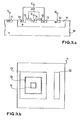
Les figures 3.a et 3.b montrent une variante du dispositif précédent dans laquelle la diffusion de collecteur 13 entoure complètement la diffusion d'émetteur 14. La figure 3.b montre la disposition de la grille 16 et des diffusions 12, 13 et 14 réalisées dans le caisson 11. Un tel arrangement permet d'avantager le transistor bipolaire latéral au détriment du transistor au substrat et d'obtenir des valeurs typiques du gain en courant β de l'ordre de 50 avec un courant d'émetteur 1Ede 1 µA.FIGS. 3.a and 3.b show a variant of the previous device in which the
L'obtention d'un gain aussi élevé montre la possibilité d'utiliser de telles structures en combinaison avec des transistors MOS notamment pour des applications analogiques. Les structures bipolaires offrent l'avantage, outre d'une caractéristique exponentielle du courant d'émetteur en fonction de la tension émetteur-base, d'un meilleur appariement, d'une meilleure reproductibilité et d'une plus faible composante de bruit en basse fréquence que les structures MOS.Obtaining such a high gain shows the possibility of using such structures in combination with MOS transistors, in particular for analog applications. Bipolar structures offer the advantage, in addition to an exponential characteristic of the emitter current as a function of the emitter-base voltage, of better matching, better reproducibility and a lower noise component at low frequency than MOS structures.
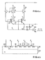
Les figures suivantes montrent plusieurs exemples de circuits, réalisables en technologie CMOS, incorporant des transistors MOS et des transistors bipolaires selon la présente invention. La figure 4.a représente un miroir de courant où I1 est le courant d'entrée et 12 le courant de sortie. Les transistors T0, T1 et T2 sont des transistors MOS à canal n tandis que Q1 et Q2 sont des transistors bipolaires selon l'invention, le symbole utilisé étant représenté à la figure 2.c. Le transistor MOS TO fournit le courant de base des transistors Q1 et Q2. Ces derniers sont connectés chacun en série avec un transistor MOS, soit T1 et T2 en série avec Q1 et Q2 respectivement. Les émetteurs de Q1 et Q2 sont reliés à la borne négative de la source d'alimentation. Le drain de TO ainsi que le substrat dans lequel le circuit est réalisé sont reliés à la borne positive de la source d'alimentation. Les grilles de Q1 et Q2 sont polarisées négativement par rapport à l'émetteur grâce au circuit de "clampage" constitué par les diodes 101 et 102 et les capacités 100 et 103 et alimenté par un signal carré appliqué sur la borne 110. Si les transistors T1 et T2 d'une part, Q1 et Q2 d'autre part, sont identiques le courant de sortie 12 est égal au courant d'entrée 11. La figure 4.b montre l'implantation possible des transistors T1 et Q1 du circuit de la figure 4.a. Le substrat 200 de type n est relié à la borne positive de l'alimentation par l'intermédiaire d'une diffusion de type n+. Dans le caisson 210 de type p, le transistor Q1 est réalisé avec une structure concentrique de même que le transistor T1. Le caisson sert d'électrode de base pour le transistor Q1. Les transistors T2 et Q2, de même que d'autres couples de transistors Ti et Qi, peuvent être réalisés de la même façon dans le caisson 210. La symétrie mesurée, à savoir l'égalité des courants 11 et 12, d'un tel miroir de courant est quatre a cinq fois meilleure que celle d'un circuit équivalent travaillant avec le même courant d'entrée I1 et n'utilisant que des transistors MOS.The following figures show several examples of circuits, achievable in CMOS technology, incorporating MOS transistors and bipolar transistors according to the present invention. Figure 4.a shows a current mirror where I1 is the input current and 12 the output current. The transistors T0, T1 and T2 are n-channel MOS transistors while Q1 and Q2 are bipolar transistors according to the invention, the symbol used being represented in FIG. 2.c. The MOS transistor TO supplies the basic current of the transistors Q1 and Q2. These are each connected in series with a MOS transistor, ie T1 and T2 in series with Q1 and Q2 respectively. The transmitters of Q1 and Q2 are connected to the negative terminal of the power source. The TO drain and the substrate in which the circuit is made are connected to the positive terminal of the power source. The gates of Q1 and Q2 are negatively polarized with respect to the transmitter thanks to the "clamping" circuit constituted by the
La figure 5 montre un autre miroir de courant dans lequel les transistors bipolaires sont réalisés directement dans le substrat de type n; ces transistors bipolaires étant du type p-n-p. Les électrodes de grille G de Q3 et Q4 sont portées à un potentiel plus positif que celui du substrat (base de Q3 et Q4) soit à l'aide d'une source extérieure au circuit, soit en utilisant un circuit de "clampage" semblable à celui de la figure 4.a. Ce potentiel appliqué en G sert à produire un courant IR à travers la résistance R. Ce courant IR est égal à la somme du courant I3, produit par T3 et T4, et des courants d'émetteur de Q3 et Q4. Si l'on applique une tension U1 entre le collecteur de Q3 et la borne d'alimentation négative du circuit et si les transistors Q3 et Q4 sont identiques, on obtient sur le collecteur de Q4 un courant de sortie 12 égal au courant de collecteur I1 de Q3.FIG. 5 shows another current mirror in which the bipolar transistors are produced directly in the n-type substrate; these bipolar transistors being of the pnp type. The gate electrodes G of Q3 and Q4 are brought to a more positive potential than that of the substrate (base of Q3 and Q4) either using a source external to the circuit, or by using a similar "clamping" circuit. to that of figure 4.a. This potential applied in G is used to produce a current I R through the resistance R. This current I R is equal to the sum of the current I 3 , produced by T3 and T4, and the emitter currents of Q3 and Q4. If a voltage U 1 is applied between the collector of Q3 and the negative supply terminal of the circuit and if the transistors Q3 and Q4 are identical, one obtains on the collector of Q4 an output current 12 equal to the collector current I1 of Q3.
La figure 6 montre un circuit, pouvant servir de source de courant, qui tire avantage du bon appariement et de la caractéristique exponentielle des transistors bipolaires. En négligeant les courants de base des transistors Q5 à Q7, les courants de collecteur I1 et 12 des transistors Q5 et Q6 respectivement sont liés par la relation
![]()
![]()
![]()
![]()
![]()
![]()
La figure 7 montre une variante du circuit de la figure 6, capable de fournir une tension de référence VR indépendante de la température. Comme dans le cas de la figure 6, si V1 représente la tension aux bornes de la résistance R1 et si les transistors MOS T7 et T8 sont identiques, on a la relation: V1 = UT.ln K", dans laquelle K" représente le rapport des surfaces des transistors bipolaires Q9 et Q8. On en déduit:![]()
![]()
La figure 8 montre un schéma d'amplificateur différentiel tirant partie du faible bruit et du bon appariement des transistors bipolaires selon l'invention. Le schéma de principe de cet amplificateur est bien connu. Les deux transistors bipolaires Q10 et Q11 sont polarisés par le miroir de courant formé par les transistors MOS T11 et T12 et alimenté par un courant de polarisation 10. Les deux transistors MOS T9 et T10, également arrangés en miroir de courant, constituent une charge pour les transistors Q10 et Q11. Si le potentiel des entrées E et E- de l'amplificateur différentiel est suffisamment élevé, la grille G des transistors Q10 et Q11 peut être reliée directement à la borne d'alimentation négative du circuit, ce qui élimine la nécessité d'une source d'alimentation supplémentaire. La borne SO constitue la sortie de cet amplificateur différentiel.FIG. 8 shows a diagram of a differential amplifier taking advantage of the low noise and the good pairing of the bipolar transistors according to the invention. The block diagram of this amplifier is well known. The two bipolar transistors Q10 and Q11 are polarized by the current mirror formed by the MOS transistors T11 and T12 and supplied by a bias current 10. The two MOS transistors T9 and T10, also arranged in current mirror, constitute a load for transistors Q10 and Q11. If the potential of the inputs E and E - of the differential amplifier is sufficiently high, the gate G of the transistors Q10 and Q11 can be connected directly to the negative supply terminal of the circuit, which eliminates the need for a source d additional food. The SO terminal constitutes the output of this differential amplifier.
Bien que l'invention ait été décrite dans le cadre d'une technologie utilisant un substrat de type n et plus particulièrement d'une technologie CMOS, elle n'est nullement limitée aux exemples d'application décrits. Il est clair, en effet, que l'invention est encore applicable dans le cas d'une technologie MOS basée sur l'utilisation d'un substrat de type p et de caissons de type n.Although the invention has been described in the context of a technology using an n-type substrate and more particularly of a CMOS technology, it is in no way limited to the examples of application described. It is clear, in fact, that the invention is still applicable in the case of an MOS technology based on the use of a p-type substrate and n-type wells.
Claims (8)
Applications Claiming Priority (2)
| Application Number | Priority Date | Filing Date | Title |
|---|---|---|---|
| CH2474/82 | 1982-04-23 | ||
| CH2474/82A CH648434A5 (en) | 1982-04-23 | 1982-04-23 | SEMICONDUCTOR DEVICE HAVING AN OPERATING CHARACTERISTIC OF A BIPOLAR TRANSISTOR AND M0S CIRCUIT INCORPORATING SUCH A DEVICE. |
Publications (2)
| Publication Number | Publication Date |
|---|---|
| EP0093086A2 true EP0093086A2 (en) | 1983-11-02 |
| EP0093086A3 EP0093086A3 (en) | 1985-10-02 |
Family
ID=4234614
Family Applications (1)
| Application Number | Title | Priority Date | Filing Date |
|---|---|---|---|
| EP83810169A Withdrawn EP0093086A3 (en) | 1982-04-23 | 1983-04-22 | Bipolar semi-conductor device and mos circuit with such a device |
Country Status (4)
| Country | Link |
|---|---|
| EP (1) | EP0093086A3 (en) |
| JP (1) | JPS58207672A (en) |
| CA (1) | CA1245372A (en) |
| CH (1) | CH648434A5 (en) |
Cited By (6)
| Publication number | Priority date | Publication date | Assignee | Title |
|---|---|---|---|---|
| WO1986004196A1 (en) * | 1984-12-29 | 1986-07-17 | Licencia Találmányokat Értékesito^" És Innovációs | Active circuit element |
| EP0188401A2 (en) * | 1985-01-17 | 1986-07-23 | Centre Electronique Horloger S.A. | Reference voltage source |
| EP0351634A2 (en) * | 1988-07-20 | 1990-01-24 | TEMIC TELEFUNKEN microelectronic GmbH | Semiconductor circuit for fast switching processes |
| US4965872A (en) * | 1988-09-26 | 1990-10-23 | Vasudev Prahalad K | MOS-enhanced, self-aligned lateral bipolar transistor made of a semiconductor on an insulator |
| EP0700090A1 (en) * | 1994-08-19 | 1996-03-06 | Kabushiki Kaisha Toshiba | Semiconductor integrated circuit comprising a current mirror circuit |
| US7217609B2 (en) | 2002-02-13 | 2007-05-15 | Infineon Technologies Ag | Semiconductor fabrication process, lateral PNP transistor, and integrated circuit |
Citations (2)
| Publication number | Priority date | Publication date | Assignee | Title |
|---|---|---|---|---|
| GB1252362A (en) * | 1969-03-11 | 1971-11-03 | ||
| US3958267A (en) * | 1973-05-07 | 1976-05-18 | National Semiconductor Corporation | Current scaling in lateral pnp structures |
Family Cites Families (5)
| Publication number | Priority date | Publication date | Assignee | Title |
|---|---|---|---|---|
| JPS5320872B1 (en) * | 1967-11-30 | 1978-06-29 | ||
| JPS50158285A (en) * | 1974-06-10 | 1975-12-22 | ||
| JPS5268382A (en) * | 1975-12-05 | 1977-06-07 | Hitachi Ltd | Semiconductor circuit unit |
| JPS52105783A (en) * | 1976-03-03 | 1977-09-05 | Hitachi Ltd | Semicondcutor unit |
| JPS5588372A (en) * | 1978-12-26 | 1980-07-04 | Sanyo Electric Co Ltd | Lateral type transistor |
-
1982
- 1982-04-23 CH CH2474/82A patent/CH648434A5/en not_active IP Right Cessation
-
1983
- 1983-04-22 CA CA000426527A patent/CA1245372A/en not_active Expired
- 1983-04-22 EP EP83810169A patent/EP0093086A3/en not_active Withdrawn
- 1983-04-22 JP JP7017583A patent/JPS58207672A/en active Pending
Patent Citations (2)
| Publication number | Priority date | Publication date | Assignee | Title |
|---|---|---|---|---|
| GB1252362A (en) * | 1969-03-11 | 1971-11-03 | ||
| US3958267A (en) * | 1973-05-07 | 1976-05-18 | National Semiconductor Corporation | Current scaling in lateral pnp structures |
Non-Patent Citations (3)
| Title |
|---|
| IBM TECHNICAL DISCLOSURE BULLETIN, vol. 15, no. 8, janvier 1973, pages 2571-2572, New York, US; W.L. BLOSE et al.: "Complimentary BI-FET logic circuitry" * |
| IBM TECHNICAL DISCLOSURE BULLETIN, vol. 17, no. 4, septembre 1974, page 1041, New York, US; H.M. DALAL et al.: "Gate controlled bistable bipolar transistor" * |
| IEEE INTERNATIONAL SOLID STATE CIRCUITS CONFERENCE, vol. 20, no. 20, février 1977, pages 224-225, IEEE, New York, US; S.R. COMBS et al.: "Advanced technology. Bimodal MOS-bipolar monolithic kitchip array" * |
Cited By (11)
| Publication number | Priority date | Publication date | Assignee | Title |
|---|---|---|---|---|
| WO1986004196A1 (en) * | 1984-12-29 | 1986-07-17 | Licencia Találmányokat Értékesito^" És Innovációs | Active circuit element |
| EP0188401A2 (en) * | 1985-01-17 | 1986-07-23 | Centre Electronique Horloger S.A. | Reference voltage source |
| EP0188401A3 (en) * | 1985-01-17 | 1986-09-10 | Centre Electronique Horloger S.A. | Reference voltage source |
| US4672304A (en) * | 1985-01-17 | 1987-06-09 | Centre Electronique Horloger S.A. | Reference voltage source |
| EP0351634A2 (en) * | 1988-07-20 | 1990-01-24 | TEMIC TELEFUNKEN microelectronic GmbH | Semiconductor circuit for fast switching processes |
| EP0351634A3 (en) * | 1988-07-20 | 1991-02-27 | TEMIC TELEFUNKEN microelectronic GmbH | Semiconductor circuit for fast switching processes |
| US5036233A (en) * | 1988-07-20 | 1991-07-30 | Telefunken Electronic Gmbh | Integrated semiconductor circuit having a unidirectional semiconductor component for preventing saturation of bipolar transistors |
| US4965872A (en) * | 1988-09-26 | 1990-10-23 | Vasudev Prahalad K | MOS-enhanced, self-aligned lateral bipolar transistor made of a semiconductor on an insulator |
| EP0700090A1 (en) * | 1994-08-19 | 1996-03-06 | Kabushiki Kaisha Toshiba | Semiconductor integrated circuit comprising a current mirror circuit |
| US5834814A (en) * | 1994-08-19 | 1998-11-10 | Kabushiki Kaisha Toshiba | Semiconductor integrated circuit |
| US7217609B2 (en) | 2002-02-13 | 2007-05-15 | Infineon Technologies Ag | Semiconductor fabrication process, lateral PNP transistor, and integrated circuit |
Also Published As
| Publication number | Publication date |
|---|---|
| CH648434A5 (en) | 1985-03-15 |
| JPS58207672A (en) | 1983-12-03 |
| EP0093086A3 (en) | 1985-10-02 |
| CA1245372A (en) | 1988-11-22 |
Similar Documents
| Publication | Publication Date | Title |
|---|---|---|
| EP0432058B1 (en) | Dynamic isolation circuit for integrated circuits | |
| CH415867A (en) | Integrated microminiature semiconductor circuit | |
| FR2636778A1 (en) | MOS COMPOSITE TRANSISTOR AND APPLICATION TO A FREE WHEEL DIODE | |
| FR2492165A1 (en) | DEVICE FOR PROTECTION AGAINST LEAKAGE CURRENTS IN INTEGRATED CIRCUITS | |
| EP0380168A1 (en) | Integrated semiconductor device comprising a field-effect transistor with an isolated gate biased at a high level | |
| JPS6118343B2 (en) | ||
| FR2490874A1 (en) | TRANSISTORS OF THE ISLE GRID TYPE | |
| EP0006474A1 (en) | Method of compensating for the voltage coefficient of ion-implanted or diffused semiconductor resistors | |
| EP0543745B1 (en) | MOS transistor with integrated zener diode protection | |
| EP0305253B1 (en) | Double heterojunction microwave transistor | |
| FR3003996A1 (en) | METHOD FOR CONTROLLING AN INTEGRATED CIRCUIT | |
| EP0614232A1 (en) | Reference diode in bipolar integrated circuit | |
| EP0780952B1 (en) | Monolithic and static current limiter and circuit breaker | |
| FR2820882A1 (en) | THREE TRANSISTOR PHOTODETECTOR | |
| FR2507819A1 (en) | OVERLOAD PROTECTION DEVICE FOR INTEGRATED CIRCUIT AND INTEGRATED OVERLOAD PROTECTION CIRCUIT | |
| EP0093086A2 (en) | Bipolar semi-conductor device and MOS circuit with such a device | |
| US3448397A (en) | Mos field effect transistor amplifier apparatus | |
| EP0737003B1 (en) | CCD register readout amplifier | |
| FR2542946A1 (en) | DIFFERENTIAL AMPLIFIER WITH BIPOLAR TRANSISTORS PRODUCED IN CMOS TECHNOLOGY | |
| FR2503933A1 (en) | INTEGRATED CIRCUIT COMPRISING A NETWORK OF TRANSISTORS | |
| FR2576431A1 (en) | REFERENCE VOLTAGE GENERATING CIRCUIT | |
| FR2561470A1 (en) | TRANSVERSE FILTER WITH CHARGE COUPLING | |
| EP0546919B1 (en) | Heterojunction bipolar transistor insensitive to external temperature variation and associated integrated circuit | |
| EP0129470A1 (en) | Solid state photosensitive device | |
| EP0737002A1 (en) | CCD readout register with multiple outputs |
Legal Events
| Date | Code | Title | Description |
|---|---|---|---|
| PUAI | Public reference made under article 153(3) epc to a published international application that has entered the european phase |
Free format text: ORIGINAL CODE: 0009012 |
|
| AK | Designated contracting states |
Designated state(s): DE FR GB IT NL SE |
|
| PUAL | Search report despatched |
Free format text: ORIGINAL CODE: 0009013 |
|
| AK | Designated contracting states |
Designated state(s): DE FR GB IT NL SE |
|
| 17P | Request for examination filed |
Effective date: 19860127 |
|
| 17Q | First examination report despatched |
Effective date: 19880201 |
|
| STAA | Information on the status of an ep patent application or granted ep patent |
Free format text: STATUS: THE APPLICATION IS DEEMED TO BE WITHDRAWN |
|
| 18D | Application deemed to be withdrawn |
Effective date: 19900629 |
|
| APAF | Appeal reference modified |
Free format text: ORIGINAL CODE: EPIDOSCREFNE |
|
| RIN1 | Information on inventor provided before grant (corrected) |
Inventor name: VITTOZ, ERIC A. |