EP0614232A1 - Reference diode in bipolar integrated circuit - Google Patents
Reference diode in bipolar integrated circuit Download PDFInfo
- Publication number
- EP0614232A1 EP0614232A1 EP94410011A EP94410011A EP0614232A1 EP 0614232 A1 EP0614232 A1 EP 0614232A1 EP 94410011 A EP94410011 A EP 94410011A EP 94410011 A EP94410011 A EP 94410011A EP 0614232 A1 EP0614232 A1 EP 0614232A1
- Authority
- EP
- European Patent Office
- Prior art keywords
- type
- conductivity
- diode
- deep
- region
- Prior art date
- Legal status (The legal status is an assumption and is not a legal conclusion. Google has not performed a legal analysis and makes no representation as to the accuracy of the status listed.)
- Granted
Links
- 238000009792 diffusion process Methods 0.000 claims abstract description 35
- 239000000758 substrate Substances 0.000 claims description 10
- 238000002955 isolation Methods 0.000 claims description 5
- 238000004519 manufacturing process Methods 0.000 description 9
- 238000001465 metallisation Methods 0.000 description 9
- 238000010586 diagram Methods 0.000 description 4
- 230000008901 benefit Effects 0.000 description 3
- 230000001174 ascending effect Effects 0.000 description 2
- ZOXJGFHDIHLPTG-UHFFFAOYSA-N Boron Chemical compound [B] ZOXJGFHDIHLPTG-UHFFFAOYSA-N 0.000 description 1
- 229910052796 boron Inorganic materials 0.000 description 1
- 230000015556 catabolic process Effects 0.000 description 1
- 238000007796 conventional method Methods 0.000 description 1
- 230000007423 decrease Effects 0.000 description 1
- 239000006185 dispersion Substances 0.000 description 1
- 230000007717 exclusion Effects 0.000 description 1
- 238000002513 implantation Methods 0.000 description 1
- 238000012986 modification Methods 0.000 description 1
- 230000004048 modification Effects 0.000 description 1
- 230000000630 rising effect Effects 0.000 description 1
- 239000004065 semiconductor Substances 0.000 description 1
Images

Classifications
-
- H—ELECTRICITY
- H01—ELECTRIC ELEMENTS
- H01L—SEMICONDUCTOR DEVICES NOT COVERED BY CLASS H10
- H01L27/00—Devices consisting of a plurality of semiconductor or other solid-state components formed in or on a common substrate
- H01L27/02—Devices consisting of a plurality of semiconductor or other solid-state components formed in or on a common substrate including semiconductor components specially adapted for rectifying, oscillating, amplifying or switching and having potential barriers; including integrated passive circuit elements having potential barriers
- H01L27/04—Devices consisting of a plurality of semiconductor or other solid-state components formed in or on a common substrate including semiconductor components specially adapted for rectifying, oscillating, amplifying or switching and having potential barriers; including integrated passive circuit elements having potential barriers the substrate being a semiconductor body
- H01L27/06—Devices consisting of a plurality of semiconductor or other solid-state components formed in or on a common substrate including semiconductor components specially adapted for rectifying, oscillating, amplifying or switching and having potential barriers; including integrated passive circuit elements having potential barriers the substrate being a semiconductor body including a plurality of individual components in a non-repetitive configuration
- H01L27/0611—Devices consisting of a plurality of semiconductor or other solid-state components formed in or on a common substrate including semiconductor components specially adapted for rectifying, oscillating, amplifying or switching and having potential barriers; including integrated passive circuit elements having potential barriers the substrate being a semiconductor body including a plurality of individual components in a non-repetitive configuration integrated circuits having a two-dimensional layout of components without a common active region
- H01L27/0641—Devices consisting of a plurality of semiconductor or other solid-state components formed in or on a common substrate including semiconductor components specially adapted for rectifying, oscillating, amplifying or switching and having potential barriers; including integrated passive circuit elements having potential barriers the substrate being a semiconductor body including a plurality of individual components in a non-repetitive configuration integrated circuits having a two-dimensional layout of components without a common active region without components of the field effect type
- H01L27/0676—Devices consisting of a plurality of semiconductor or other solid-state components formed in or on a common substrate including semiconductor components specially adapted for rectifying, oscillating, amplifying or switching and having potential barriers; including integrated passive circuit elements having potential barriers the substrate being a semiconductor body including a plurality of individual components in a non-repetitive configuration integrated circuits having a two-dimensional layout of components without a common active region without components of the field effect type comprising combinations of diodes, or capacitors or resistors
-
- H—ELECTRICITY
- H01—ELECTRIC ELEMENTS
- H01L—SEMICONDUCTOR DEVICES NOT COVERED BY CLASS H10
- H01L29/00—Semiconductor devices specially adapted for rectifying, amplifying, oscillating or switching and having potential barriers; Capacitors or resistors having potential barriers, e.g. a PN-junction depletion layer or carrier concentration layer; Details of semiconductor bodies or of electrodes thereof ; Multistep manufacturing processes therefor
- H01L29/66—Types of semiconductor device ; Multistep manufacturing processes therefor
- H01L29/86—Types of semiconductor device ; Multistep manufacturing processes therefor controllable only by variation of the electric current supplied, or only the electric potential applied, to one or more of the electrodes carrying the current to be rectified, amplified, oscillated or switched
- H01L29/861—Diodes
- H01L29/866—Zener diodes
Definitions
- the present invention relates to the field of bipolar integrated circuits, and more particularly the production of avalanche diodes intended to serve as a voltage reference in such circuits.
- Avalanche diodes have been studied at length, and it is known, when producing discrete components, to obtain satisfactory avalanche diodes.
- many constraints are imposed, namely that a large number of elementary components are produced simultaneously and that all of these components must be produced using a minimum of steps technological.
- This component comprises a first avalanche diode Z1 in series with resistance R1.
- a second diode Z2 is arranged in parallel on the series assembly of the diode Z1 and of the resistor R1.
- the resistance R1 often has a non-negligible value, for example of the order of 400 to 1000 ⁇ .
- the diode Z2 normally, has a higher avalanche threshold than that of diode Z1 and does not intervene.
- the voltage drop in resistor R1 increases and when this voltage drop exceeds the difference in avalanche voltages between diodes Z2 and Z1, diode Z2 can at its turn enter avalanche.
- Avalanche diodes are known as described in European patent applications 0314399 and 0017022 which have the advantage that the stray diode Z2 has a very high avalanche voltage, of the order of 100 volts or more, while the diode Z1 has an avalanche voltage of the order of 6 V. Thus, the stray diode Z2 no longer intervenes.
- these diodes still have certain drawbacks. As pointed out above, their manufacturing process must use only steps which are already used in the manufacture of a conventional bipolar integrated circuit. Thus, the doping levels of the various layers of these diodes are imposed by technology and are not optimized. As a result, the series resistance R1 of the diode can be of the order of 100 to 400 ohms. In addition, the diode has a temperature coefficient, that is to say a variation of its breakdown voltage as a function of the temperature, which is of the order of 2.8 mV / ° C. These two characteristics (internal resistance and non-negligible temperature coefficient) constitute significant drawbacks for producing a reference diode, the voltage of which we would like to be defined with precision whatever the current flowing through it and the temperature of the integrated circuit. .
- FIG. 2 An example of such a circuit is illustrated in FIG. 2.
- This circuit is connected to the terminals of a supply voltage, for example between a positive supply Vcc and the ground G.
- a first branch consists of the series connection of a current source I and an NPN transistor T1.
- a second branch comprises the series connection of an NPN transistor T2, of an avalanche diode (represented in the form of a pure avalanche diode Z in series with an internal resistance RZ) and of a resistance R.
- the base of the transistor T2 is connected to the collector of the transistor T1 and the base of the transistor T1 is connected to the connection point between the avalanche diode Z-RZ and the resistor R.
- the reference voltage depends on the ratio between the series resistance Rz of the avalanche diode and the resistance R which defines the current in this diode.
- Rz is generally not negligible before R, the absolute value of the reference voltage will be subject to variations in the Rz / R ratio and the same will apply to temperature drift. This results in poor reproducibility of this reference voltage.
- an object of the present invention is to provide a new reference diode structure applicable to a bipolar integrated circuit and not using any manufacturing step other than the steps normally provided for in a bipolar integrated circuit.
- Another object of the present invention is to provide a reference diode compensated in current and in temperature.
- the present invention provides an embodiment of the aforementioned resistance R which makes it possible to ensure that the ratio Rz / R remains insensitive to manufacturing dispersions.
- the present invention provides a reference diode formed in a box isolated from an epitaxial layer of a first type of conductivity covering a substrate of the second type of conductivity.
- This reference diode includes: on the one hand, an avalanche diode comprising, at the bottom of the box, a deep region of the second type of conductivity with a high level of doping, under and overflowing with which a buried layer of the first type of conductivity is formed; a first deep diffusion of the second type of conductivity joining a central part of said deep region; a second deep diffusion of the second type of conductivity joining the periphery of said deep region; a surface region of the first type of conductivity with a high doping level covering the surface of the first deep diffusion and forming with it an avalanche junction; a first electrode in contact with the surface of the surface region; and a second electrode in contact with the surface of the second deep diffusion; on the other hand, in the same box, at least one other structure identical to that of this diode
- the second deep diffusion has an annular shape.
- the isolation of the box is ensured by the meeting of a foundation of the second type of conductivity formed in the substrate and of a third deep diffusion of the second type of conductivity starting from the external surface. of the epitaxial layer, and said deep region is of the same nature as said foundation.
- the present invention also provides a reference diode comprising, between a high power source and ground, a first branch constituted by the series connection of a current source and a first transistor, a second branch comprising the connection in series of a second transistor, of the avalanche diode and of the above-mentioned resistor (s), means of connection between the base of the second transistor and the emitter of the first, means of connection between the base of the first transistor and the connection point of the avalanche diode and the resistor (s).
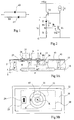
- the present invention uses an avalanche diode formed in a bipolar technology circuit comprising an epitaxial layer 2 of type N covering a substrate 1 of type P. More particularly, the diode is formed in a box 10 of the epitaxial layer 2 delimited laterally by an isolation wall of type P 11 and the bottom of which corresponds to a buried layer 3 of type N.
- the isolation wall 11 is formed by the encounter of a deep diffusion 12 descending from the surface of the epitaxial layer 2 and from a diffusion 13 rising from a P-type foundation initially formed on the surface of the substrate 1 before the production of the epitaxial layer 2.
- the active junction of the diode is formed of the junction between a downward deep diffusion of type P 15 and a surface region of type N heavily doped 16. Region 16, outside of its junction with diffusion P 15 is surrounded by a lightly doped N-type region corresponding to the epitaxial layer.
- the contact with the region N+ 16 is taken up by a metallization of cathode K.
- the contact with the region P 45 is taken up by a strongly doped P-type deep diffusion 20 corresponding to an ascending diffusion formed from a P-type foundation implanted in the substrate above the buried layer 3 of N+ type.
- This foundation P is formed at the same time as the foundations of the ascending isolation diffusions 13.
- deep diffusions 21 are formed from the surface of the epitaxial layer and join the deep layer 20.
- the diffusions 21 are formed at the same time time that the diffusions 22 and 25.
- a metallization of anode A makes it possible to resume contact with the upper part of the diffusion 21.
- this box is polarized to be isolated by junction of the substrate.
- the box N 10 must be positively polarized. This is achieved by forming a region 23 with a high level of N-type doping in a portion of the upper surface of the well 10, this region being in contact with a metallization 24 which is connected to a more positive potential than that to which the substrate 1. Since the diode functions as an avalanche diode, its terminal K is normally at a more positive potential than its terminal A and the metallization 24 can be connected to terminal K.
- FIG. 3B shows a schematic top view corresponding to Figure 3A and the same parts as in Figure 3A are designated by the same references. It will be noted that the region 21 for resumption of contact with the deep layer 20 is preferably a circular region completely surrounding the region N+ 16 of the cathode.
- FIGS. 4A and 4B show in section and in top view, respectively, an association according to the present invention of the avalanche diode described above and of resistors intended to constitute the resistor R described in relation to FIG. 2.
- the same elements as in FIGS. 3A and 3B are designated by the same references.
- FIG. 4A a diode structure strictly identical to that of FIG. 3A.
- this diode structure is repeated twice, omitting the diffusion N+ 16, to form two resistance structures R 'and R' 'having substantially the same resistance value Rz as the diode.
- the resistor R ′ comprises a deep layer 30, a central deep diffusion 31 joining the deep layer 30 and a deep diffusion 32 in a ring also joining this deep layer.
- a contact 33 is made with the region 31 and a contact 34 with the surface of the ring 32.
- the second resistor R '' comprises corresponding regions 40, 41, 42, 43 and 44.
- the terminal A of the diode is connected to the metallization 33 of the resistor R 'and to the base terminal B of the transistor T1.
- the metallization 34 of the resistor R ' is connected to the metallization 43 of the resistor R' 'whose metallization 44 is connected to the ground terminal G.
- FIG. 4B The top view of FIG. 4B allows a better view of the various metallizations.
- Figure 5 shows the diagram of Figure 2 with indication of the resistors R 'and R' 'both having the same value Rz as the series resistance of the diode Vz.
- the present invention is susceptible of various variants which will appear to those skilled in the art.
- a circular shape is shown in top view with a central cathode electrode and an annular anode electrode, this structure could have any other desired shape.
- the various regions could be square regions nested one inside the other, rectangular regions, fingered regions, etc.
- the thickness of the epitaxial layer 2 can be of the order of 16 ⁇ m.
- the diffusion depth of the deep diffusions 12, 21, 31, 32, 41, 42 can be of the order of 6 ⁇ m, the diffusion 15 having a doping level at its interface with the region N 16 of the order of 3.1018 atoms / cm3, this N 16 region having a doping level of the order of 3.1020 atoms / cm3.
- the deep layers 20, 30, 40 and 13 can result from an implantation of boron with a dose of 2.5 1014 atoms / cm2 under an energy of 180 keV.
- the zones 15, 31 and 41 have a diameter of 10 ⁇ m
- the zones 21, 32 and 42 have a diameter of 48 ⁇ m
- the outer contour of these zones is a 76 ⁇ m square side
- zone 16 has a diameter of 10 ⁇ m.
- the avalanche voltage Vz is 6.7 V ⁇ 250 mV and the series resistance Rz is 350 ⁇ .
- the reference voltage Vr obtained ( Figure 6) is 7.9 V ⁇ 300 mV.
- the present invention is susceptible of numerous variants and modifications which will appear to those skilled in the art.
- certain aspects of implementation have been shown in a simplified manner.
- many common improvements will be adopted.
- the upper surface of different layers such as layers 21, 31, 32, 41, 42 will be overdoped to improve the contacts.
Landscapes
- Engineering & Computer Science (AREA)
- Power Engineering (AREA)
- Microelectronics & Electronic Packaging (AREA)
- Physics & Mathematics (AREA)
- Condensed Matter Physics & Semiconductors (AREA)
- General Physics & Mathematics (AREA)
- Computer Hardware Design (AREA)
- Ceramic Engineering (AREA)
- Bipolar Integrated Circuits (AREA)
- Bipolar Transistors (AREA)
Abstract
Description
La présente invention concerne le domaine des circuits intégrés bipolaires, et plus particulièrement la réalisation de diodes à avalanche destinées à servir de référence de tension dans de tels circuits.The present invention relates to the field of bipolar integrated circuits, and more particularly the production of avalanche diodes intended to serve as a voltage reference in such circuits.
Les diodes à avalanche ont été longuement étudiées, et l'on sait, quand on réalise des composants discrets, obtenir des diodes à avalanche satisfaisantes. Néanmoins, dans le cadre de la réalisation d'un circuit intégré, de nombreuses contraintes sont imposées, à savoir que l'on réalise simultanément un grand nombre de composants élémentaires et que tous ces composants doivent être réalisés en recourant à un minimum d'étapes technologiques.Avalanche diodes have been studied at length, and it is known, when producing discrete components, to obtain satisfactory avalanche diodes. However, in the context of the production of an integrated circuit, many constraints are imposed, namely that a large number of elementary components are produced simultaneously and that all of these components must be produced using a minimum of steps technological.
Ainsi, de façon générale, quand on cherche à réaliser une diode à avalanche enterrée et isolée du substrat, Z, on obtient en fait un composant dont le schéma équivalent est illustré en figure 1. Ce composant comprend une première diode à avalanche Z1 en série avec une résistance R1. Une deuxième diode Z2 est disposée en parallèle sur l'ensemble en série de la diode Z1 et de la résistance R1.Thus, in general, when one seeks to produce a buried avalanche diode isolated from the substrate, Z, one in fact obtains a component whose equivalent diagram is illustrated in FIG. 1. This component comprises a first avalanche diode Z1 in series with resistance R1. A second diode Z2 is arranged in parallel on the series assembly of the diode Z1 and of the resistor R1.
En pratique, la résistance R1 a souvent une valeur non négligeable, par exemple de l'ordre de 400 à 1000 Ω. D'autre part, normalement, la diode Z2 a un seuil d'avalanche plus élevé que celui de la diode Z1 et n'intervient pas. Toutefois, quand le courant d'avalanche dans la diode Z1 augmente, la chute de tension dans la résistance R1 croit et quand cette chute de tension dépasse la différence de tensions d'avalanche entre les diodes Z2 et Z1, la diode Z2 peut à son tour entrer en avalanche.In practice, the resistance R1 often has a non-negligible value, for example of the order of 400 to 1000 Ω. On the other hand, normally, the diode Z2 has a higher avalanche threshold than that of diode Z1 and does not intervene. However, when the avalanche current in diode Z1 increases, the voltage drop in resistor R1 increases and when this voltage drop exceeds the difference in avalanche voltages between diodes Z2 and Z1, diode Z2 can at its turn enter avalanche.
On peut éviter ces divers inconvénients en prévoyant des niveaux de dopage spécifiques pour les différentes couches constituant la diode à avalanche mais alors on complique le processus technologique de fabrication et l'on ne peut plus utiliser une filière classique de fabrication de composant bipolaire.These various drawbacks can be avoided by providing specific doping levels for the different layers constituting the avalanche diode, but then the technological manufacturing process is complicated and it is no longer possible to use a conventional method for manufacturing a bipolar component.
On connait des diodes à avalanche telles que décrites dans les demandes de brevet européen 0314399 et 0017022 qui présentent l'avantage que la diode parasite Z2 a une tension d'avalanche très élevée, de l'ordre de 100 volts ou plus, tandis que la diode Z1 a une tension d'avalanche de l'ordre de 6 V. Ainsi, la diode parasite Z2 n'intervient plus.Avalanche diodes are known as described in European patent applications 0314399 and 0017022 which have the advantage that the stray diode Z2 has a very high avalanche voltage, of the order of 100 volts or more, while the diode Z1 has an avalanche voltage of the order of 6 V. Thus, the stray diode Z2 no longer intervenes.
En dépit de cet avantage, ces diodes présentent encore certains inconvénients. Comme on l'a souligné précédemment, leur processus de fabrication doit utiliser uniquement des étapes qui sont déjà utilisées dans la fabrication d'un circuit intégré bipolaire classique. Ainsi, les niveaux de dopage des diverses couches de ces diodes sont imposés par la technologie et ne sont pas optimisés. Il en résulte que la résistance série R1 de la diode peut être de l'ordre de 100 à 400 ohms. De plus, la diode présente un coefficient de température, c'est-à-dire une variation de sa tension de claquage en fonction de la température, qui est de l'ordre de 2,8 mV/°C. Ces deux caractéristiques (résistance interne et coefficient de température non négligeable) constituent des inconvénients notables pour la réalisation d'une diode de référence dont on voudrait que la tension soit définie avec précision quels que soient le courant qui la traverse et la température du circuit intégré.Despite this advantage, these diodes still have certain drawbacks. As pointed out above, their manufacturing process must use only steps which are already used in the manufacture of a conventional bipolar integrated circuit. Thus, the doping levels of the various layers of these diodes are imposed by technology and are not optimized. As a result, the series resistance R1 of the diode can be of the order of 100 to 400 ohms. In addition, the diode has a temperature coefficient, that is to say a variation of its breakdown voltage as a function of the temperature, which is of the order of 2.8 mV / ° C. These two characteristics (internal resistance and non-negligible temperature coefficient) constitute significant drawbacks for producing a reference diode, the voltage of which we would like to be defined with precision whatever the current flowing through it and the temperature of the integrated circuit. .
Etant donné que ces deux inconvénients existent à plus ou moins grande échelle dans toutes les diodes à avalanche connues, on a prévu dans l'art antérieur de former à partir d'une diode à avalanche des circuits de fourniture de tension de référence compensée en courant et en température. Un exemple d'un tel circuit est illustré en figure 2. Ce circuit est connecté aux bornes d'une tension d'alimentation, par exemple entre une alimentation positive Vcc et la masse G. Dans ce circuit, une première branche est constituée de la connexion en série d'une source de courant I et d'un transistor NPN T1. Une deuxième branche comprend la connexion en série d'un transistor NPN T2, d'une diode à avalanche (représentée sous forme d'une diode à avalanche pure Z en série avec une résistance interne RZ) et d'une résistance R. La base du transistor T2 est connectée au collecteur du transistor T1 et la base du transistor T1 est connectée au point de raccordement entre la diode à avalanche Z-RZ et la résistance R. La tension de référence recherchée Vr est prise aux bornes de la connexion en série de la diode à avalanche et de la résistance R, c'est-à-dire entre l'émetteur du transistor T2 et la masse G. Si on appelle Vbe la tension base-émetteur du transistor Tl, la tension de référence est donnée par l'expression ci-dessous :![]()
Iz étant le courant traversant la diode à avalanche.Since these two disadvantages exist on a more or less large scale in all known avalanche diodes, provision has been made in the prior art to form, from an avalanche diode, circuits for supplying reference voltage compensated with current. and in temperature. An example of such a circuit is illustrated in FIG. 2. This circuit is connected to the terminals of a supply voltage, for example between a positive supply Vcc and the ground G. In this circuit, a first branch consists of the series connection of a current source I and an NPN transistor T1. A second branch comprises the series connection of an NPN transistor T2, of an avalanche diode (represented in the form of a pure avalanche diode Z in series with an internal resistance RZ) and of a resistance R. The base of the transistor T2 is connected to the collector of the transistor T1 and the base of the transistor T1 is connected to the connection point between the avalanche diode Z-RZ and the resistor R. The desired reference voltage Vr is taken across the series connection of the avalanche diode and of the resistance R, that is to say between the emitter of the transistor T2 and the ground G. If the base-emitter voltage of the transistor Tl is called Vbe, the reference voltage is given by the expression below: ![]()
Iz being the current passing through the avalanche diode.
Le courant de base du transistor T1 étant faible, par rapport au courant Iz, on peut écrire :![]()
d'où :![]()
soit :![]()
![]()
from where : ![]()
is : ![]()
On voit que la tension de référenoe dépend du rapport entre la résistance série Rz de la diode à avalanche et la résistance R qui définit le courant dans cette diode. Rz n'étant généralement pas négligeable devant R, la valeur absolue de la tension de référence sera soumise aux variations du rapport Rz/R et il en sera de même pour la dérive en température. Il en résulte une mauvaise reproductibilité de oette tension de référence.We see that the reference voltage depends on the ratio between the series resistance Rz of the avalanche diode and the resistance R which defines the current in this diode. Rz is generally not negligible before R, the absolute value of the reference voltage will be subject to variations in the Rz / R ratio and the same will apply to temperature drift. This results in poor reproducibility of this reference voltage.
Ainsi, un objet de la présente invention est de prévoir une nouvelle structure de diode de référence applicable à un circuit intégré bipolaire et n'utilisant pas d'étape de fabrication autre que les étapes normalement prévues dans un circuit intégré bipolaire.Thus, an object of the present invention is to provide a new reference diode structure applicable to a bipolar integrated circuit and not using any manufacturing step other than the steps normally provided for in a bipolar integrated circuit.
Un autre objet de la présente invention est de prévoir une diode de référence compensée en courant et en température.Another object of the present invention is to provide a reference diode compensated in current and in temperature.
Plus particulièrement, la présente invention propose une réalisation de la résistance R susmentionnée qui permet de s'assurer que le rapport Rz/R reste insensible aux dispersions de fabrication.More particularly, the present invention provides an embodiment of the aforementioned resistance R which makes it possible to ensure that the ratio Rz / R remains insensitive to manufacturing dispersions.
Pour atteindre ces objets, la présente invention prévoit une diode de référence formée dans un caisson isolé d'une couche épitaxiée d'un premier type de conductivité recouvrant un substrat du deuxième type de conductivité. Cette diode de référence comprend :
d'une part, une diode à avalanche comportant, au fond du caisson, une région profonde du deuxième type de conductivité à haut niveau de dopage, sous et en débordement de laquelle est formée une couche enterrée du premier type de conductivité ; une première diffusion profonde du deuxième type de conductivité rejoignant une partie centrale de ladite région profonde ; une deuxième diffusion profonde du deuxième type de conductivité rejoignant la périphérie de ladite région profonde ; une région superficielle du premier type de conductivité à haut niveau de dopage recouvrant la surface de la première diffusion profonde et formant avec elle une jonction à avalanche ; une première électrode en contact avec la surface de la région superficielle ; et une deuxième électrode en contact avec la surface de la deuxième diffusion profonde ;
d'autre part, dans le même caisson, au moins une autre structure identique à celle de cette diode à l'exclusion de la région superficielle du premier type de conductivité, la première électrode étant en contact avec la surface supérieure de la première diffusion profonde, cette autre structure formant entre ses première et deuxième électrodes une résistance ; et des moyens de connexion en série de la diode et de la ou des résistances.To achieve these objects, the present invention provides a reference diode formed in a box isolated from an epitaxial layer of a first type of conductivity covering a substrate of the second type of conductivity. This reference diode includes:
on the one hand, an avalanche diode comprising, at the bottom of the box, a deep region of the second type of conductivity with a high level of doping, under and overflowing with which a buried layer of the first type of conductivity is formed; a first deep diffusion of the second type of conductivity joining a central part of said deep region; a second deep diffusion of the second type of conductivity joining the periphery of said deep region; a surface region of the first type of conductivity with a high doping level covering the surface of the first deep diffusion and forming with it an avalanche junction; a first electrode in contact with the surface of the surface region; and a second electrode in contact with the surface of the second deep diffusion;
on the other hand, in the same box, at least one other structure identical to that of this diode with the exclusion of the surface region of the first type of conductivity, the first electrode being in contact with the upper surface of the first deep diffusion , this other structure forming a resistance between its first and second electrodes; and means for connecting the diode and the resistor (s) in series.
Selon un mode de réalisation de la présente invention, la deuxième diffusion profonde a une forme annulaire.According to an embodiment of the present invention, the second deep diffusion has an annular shape.
Selon un mode de réalisation de la présente invention, l'isolement du caisson est assuré par la rencontre d'une fondation du deuxième type de conductivité formée dans le substrat et d'une troisième diffusion profonde du deuxième type de conductivité partant de la surface externe de la couche épitaxiée, et ladite région profonde est de même nature que ladite fondation.According to an embodiment of the present invention, the isolation of the box is ensured by the meeting of a foundation of the second type of conductivity formed in the substrate and of a third deep diffusion of the second type of conductivity starting from the external surface. of the epitaxial layer, and said deep region is of the same nature as said foundation.
La présente invention prévoit aussi une diode de référence comprenant, entre une source d'alimentation haute et la masse, une première branche constituée de la connexion en série d'une source de courant et d'un premier transistor, une deuxième branche comprenant la connexion en série d'un deuxième transistor, de la diode à avalanche et de la ou des résistances susmentionnées, des moyens de connexion entre la base du deuxième transistor et l'émetteur du premier, des moyens de connexion entre la base du premier transistor et le point de connexion de la diode à avalanche et de la ou des résistances.The present invention also provides a reference diode comprising, between a high power source and ground, a first branch constituted by the series connection of a current source and a first transistor, a second branch comprising the connection in series of a second transistor, of the avalanche diode and of the above-mentioned resistor (s), means of connection between the base of the second transistor and the emitter of the first, means of connection between the base of the first transistor and the connection point of the avalanche diode and the resistor (s).
Ces objets, caractéristiques et avantages ainsi que d'autres de la présente invention seront exposés en détail dans la description suivante d'un mode de réalisation particulier faite en relation avec les figures jointes parmi lesquelles :
- la figure 1 représente un schéma équivalent d'une diode à avalanche enterrée et isolée classique ;
- la figure 2 représente un montage classique de fourniture de tension de référence ;
- les figures 3A et 3B représentent une vue en coupe et une vue de dessus d'un mode de réalisation de diode à avalanche utilisée selon la présente invention ;
- les figures 4A et 4B représentent une vue en coupe et une vue de dessus d'une diode à avalanche combinée à des résistances pour former une diode de référence selon la présente invention ; et
- la figure 5 est un schéma équivalent d'une diode de référence incorporant la structure des figures 4A et 4B.
- FIG. 1 represents an equivalent diagram of a conventional buried and isolated avalanche diode;
- FIG. 2 represents a conventional arrangement for supplying reference voltage;
- Figures 3A and 3B show a sectional view and a top view of an embodiment of an avalanche diode used according to the present invention;
- FIGS. 4A and 4B show a sectional view and a top view of an avalanche diode combined with resistors to form a reference diode according to the present invention; and
- Figure 5 is an equivalent diagram of a reference diode incorporating the structure of Figures 4A and 4B.
Conformément à l'usage dans le domaine de la représentation des composants semiconducteurs, ces diverses figures sont fortement schématiques et ne sont pas dessinées à l'échelle. Notamment, les formes courbes des bords de jonction résultant des diffusions ne correspondent pas à la réalité.In accordance with the practice in the field of the representation of semiconductor components, these various figures are highly schematic and are not drawn to scale. In particular, the curved shapes of the junction edges resulting from the diffusions do not correspond to reality.
Comme le représentent les figures 3A et 3B, la présente invention utilise une diode à avalanche formée dans un circuit de technologie bipolaire comprenant une couche épitaxiée 2 de type N recouvrant un substrat 1 de type P. Plus particulièrement, la diode est formée dans un caisson 10 de la couche épitaxiée 2 délimité latéralement par un mur d'isolement de type P 11 et dont le fond correspond à une couche enterrée 3 de type N. Le mur d'isolement 11 est constitué par la rencontre d'une diffusion profonde 12 descendant à partir de la surface de la couche épitaxiée 2 et d'une diffusion 13 montant à partir d'une fondation de type P initialement formée à la surface du substrat 1 avant la réalisation de la couche épitaxiée 2.As shown in FIGS. 3A and 3B, the present invention uses an avalanche diode formed in a bipolar technology circuit comprising an
La jonction active de la diode est formée de la jonction entre une diffusion profonde descendante de type P 15 et une région superficielle de type N fortement dopée 16. La région 16, en dehors de sa jonction avec la diffusion P 15 est entourée d'une région de type N faiblement dopée correspondant à la couche épitaxiée.The active junction of the diode is formed of the junction between a downward deep diffusion of
Le contact avec la région N⁺ 16 est repris par une métallisation de cathode K. Le contact avec la région P 45 est repris par une diffusion profonde de type P fortement dopée 20 correspondant à une diffusion ascendante formée à partir d'une fondation de type P implantée dans le substrat au-dessus de la couche enterrée 3 de type N⁺. Cette fondation P est formée en même temps que les fondations des diffusions ascendantes d'isolement 13. Ensuite, des diffusions profondes 21 sont formées à partir de la surfaoe de la couche épitaxiée et rejoignent la couche profonde 20. Les diffusions 21 sont formées en même temps que les diffusions 22 et 25. Une métallisation d'anode A permet de reprendre un contact avec la partie supérieure de la diffusion 21.The contact with the region N⁺ 16 is taken up by a metallization of cathode K. The contact with the region P 45 is taken up by a strongly doped P-type
De plus, de façon classique, comme chaque fois que l'on réalise dans un circuit intégré bipolaire un composant dans un caisson, ce caisson est polarisé pour être isolé par jonction du substrat. Ainsi, le caisson N 10 doit être polarisé positivement. Ceci est réalisé en formant une région 23 à haut niveau de dopage de type N dans une portion de la surface supérieure du caisson 10, cette région étant en contact avec une métallisation 24 qui est reliée à un potentiel plus positif que celui auquel est connecté le substrat 1. La diode fonctionnant en diode à avalanche, sa borne K est normalement à un potentiel plus positif que sa borne A et la métallisation 24 peut être reliée à la borne K.In addition, conventionally, as each time that a component in a box is made in a bipolar integrated circuit, this box is polarized to be isolated by junction of the substrate. Thus, the
La figure 3B représente une vue de dessus schématique correspondant à la figure 3A et de mêmes parties qu'en figure 3A sont désignées par de mêmes références. On notera que la région 21 de reprise de contact avec la couche profonde 20 est de préférence une région circulaire entourant complètement la région N⁺ 16 de cathode.3B shows a schematic top view corresponding to Figure 3A and the same parts as in Figure 3A are designated by the same references. It will be noted that the
Les figures 4A et 4B représentent en coupe et en vue de dessus, respectivement, une association selon la présente invention de la diode à avalanche décrite précédemment et de résistances destinées à constituer la résistance R décrite en relation avec la figure 2. Dans ces figures, de mêmes éléments qu'en figures 3A et 3B sont désignés par de mêmes références.FIGS. 4A and 4B show in section and in top view, respectively, an association according to the present invention of the avalanche diode described above and of resistors intended to constitute the resistor R described in relation to FIG. 2. In these figures, the same elements as in FIGS. 3A and 3B are designated by the same references.
On retrouve à la partie gauche de la figure 4A une structure de diode strictement identique à celle de la figure 3A. Dans l'exemple de la figure 4A, cette structure de diode est répétée deux fois, en omettant la diffusion N⁺ 16, pour former deux structures de résistances R' et R'' ayant sensiblement la même valeur de résistance Rz que la diode. La résistance R' comprend une couche profonde 30, une diffusion profonde centrale 31 rejoignant la couche profonde 30 et une diffusion profonde 32 en anneau rejoignant également cette couche profonde. Un contact 33 est pris avec la région 31 et un contact 34 avec la surface de l'anneau 32. De même, la deuxième résistance R'' comprend des régions correspondantes 40, 41, 42, 43 et 44. La borne A de la diode est reliée à la métallisation 33 de la résistance R' et à la borne de base B du transistor T1. La métallisation 34 de la résistance R' est reliée à la métallisation 43 de la résistance R'' dont la métallisation 44 est reliée à la borne de masse G.We find on the left side of FIG. 4A a diode structure strictly identical to that of FIG. 3A. In the example of FIG. 4A, this diode structure is repeated twice, omitting the diffusion N⁺ 16, to form two resistance structures R 'and R' 'having substantially the same resistance value Rz as the diode. The resistor R ′ comprises a
La vue de dessus de la figure 4B permet de mieux voir les diverses métallisations.The top view of FIG. 4B allows a better view of the various metallizations.
La figure 5 reprend le schéma de la figure 2 avec indication des résistanoes R' et R'' ayant toutes deux la même valeur Rz que la résistance série de la diode Vz.Figure 5 shows the diagram of Figure 2 with indication of the resistors R 'and R' 'both having the same value Rz as the series resistance of the diode Vz.
Avec cette structure, on a
On notera d'ailleurs que l'on aurait pu prévoir une seule résistance R ou plus de deux résistances R. Néanmoins, pour réduire la dérive en température, on préfère dans le cas de la technologie utilisée prévoir deux résistances R'. En effet, la dérive en température est alors :![]()
![]()
Dans la technologie utilisée dVz/dT = +2,8 mV/°C et dVbe/dT = -2 mV/°C. On arrive donc à :![]()
c'est-à-dire que la dérive en température est pratiquement complètement compensée. Cette compensation peut être rendue rigoureuse en choisissant l'intensité de la source de courant I en fonction de la surface du transistor T1 pour obtenir une densité de courant déterminée dans ce transistor. En effet le coefficient de température de la tension Vbe diminue lorsque la densité de courant dans l'émetteur du transistor T1 augmente.In the technology used dVz / dT = +2.8 mV / ° C and dVbe / dT = -2 mV / ° C. We therefore arrive at: ![]()
that is, the temperature drift is almost completely compensated. This compensation can be made rigorous by choosing the intensity of the current source I as a function of the surface of the transistor T1 to obtain a current density determined in this transistor. In fact, the temperature coefficient of the voltage Vbe decreases when the current density in the emitter of the transistor T1 increases.
Bien entendu, la présente invention est susceptible de diverses variantes qui apparaîtront à l'homme de l'art. Notamment, alors que l'on a représenté en vue de dessus une structure de forme circulaire avec une électrode de cathode centrale et une électrode d'anode annulaire, cette structure pourrait avoir toute autre forme souhaitée. Par exemple les diverses régions pourraient être des régions carrées emboîtées les unes dans les autres, des régions rectangulaires, des régions digitées etc.Of course, the present invention is susceptible of various variants which will appear to those skilled in the art. In particular, while a circular shape is shown in top view with a central cathode electrode and an annular anode electrode, this structure could have any other desired shape. For example, the various regions could be square regions nested one inside the other, rectangular regions, fingered regions, etc.
A titre d'exemple de valeurs numériques, l'épaisseur de la couche épitaxiée 2 peut être de l'ordre de 16 µm. La profondeur de diffusion des diffusions profondes 12, 21, 31, 32, 41, 42 peut être de l'ordre de 6 µm, la diffusion 15 présentant un niveau de dopage au niveau de son interface avec la région N 16 de l'ordre de 3.10¹⁸ atomes/cm³, cette région N 16 présentant un niveau de dopage de l'ordre de 3.10²⁰ atomes/cm³. Les couches profondes 20, 30, 40 et 13 peuvent résulter d'une implantation de bore avec une dose de 2,5 10¹⁴ atomes/cm² sous une énergie de 180 keV.As an example of numerical values, the thickness of the
En se reportant aux figures 4A et 4B, dans une réalisation particulière, les zones 15, 31 et 41 ont un diamètre de 10 µm, les zones 21, 32 et 42 ont un diamètre de 48 µm, le contour extérieur de ces zones est un carré de 76 µm de côté, la zone 16 a un diamètre de 10 µm. La tension d'avalanche Vz est de 6,7 V ± 250 mV et la résistance série Rz est de 350 Ω. La tension de référence Vr obtenue (figure 6) est de 7,9 V ± 300 mV.Referring to FIGS. 4A and 4B, in a particular embodiment, the
La présente invention est susceptible de nombreuses variantes et modifications qui apparaîtront à l'homme de l'art. Notamment, certains aspects de réalisation ont été représentés de façon simplifiée. En pratique, de nombreuses améliorations usuelles seront adoptées. Par exemple, la surface supérieure de différentes couches telles que les couches 21, 31, 32, 41, 42 sera surdopée pour améliorer les contacts.The present invention is susceptible of numerous variants and modifications which will appear to those skilled in the art. In particular, certain aspects of implementation have been shown in a simplified manner. In practice, many common improvements will be adopted. For example, the upper surface of different layers such as
Claims (5)
au fond du caisson, une région profonde (20) du deuxième type de conductivité à haut niveau de dopage, sous et en débordement de laquelle est formée une couche enterrée (3) du premier type de conductivité,
une première diffusion profonde (15) du deuxième type de conductivité rejoignant une partie centrale de ladite région profonde,
une deuxième diffusion profonde (21) du deuxième type de conductivité rejoignant la périphérie de ladite région profonde,
une région superficielle (16) du premier type de conductivité à haut niveau de dopage recouvrant la surface de la première diffusion profonde et formant avec elle une jonction à avalanche,
une première électrode (K) en contact avec la surface de la région superficielle, et
une deuxième électrode (A) en contact avec la surface de la deuxième diffusion profonde ; et
au moins une autre structure (31-34 ; 41-44) identique à celle de ladite diode à avalanche à l'exclusion de la région superficielle du premier type de conductivité, la première électrode (33 ; 43) étant alors en contact avec la surface supérieure de la première diffusion profonde (31 ; 41), cette autre structure formant entre ses première et deuxième électrodes (33, 34 ; 43, 44) une résistance, et
des moyens de connexion en série de la diode à avalanche et de la ou des résistances.
at the bottom of the box, a deep region (20) of the second type of conductivity with a high doping level, under and beyond which a buried layer (3) of the first type of conductivity is formed,
a first deep diffusion (15) of the second type of conductivity joining a central part of said deep region,
a second deep diffusion (21) of the second type of conductivity joining the periphery of said deep region,
a surface region (16) of the first type of conductivity with a high doping level covering the surface of the first deep diffusion and forming with it an avalanche junction,
a first electrode (K) in contact with the surface of the surface region, and
a second electrode (A) in contact with the surface of the second deep diffusion; and
at least one other structure (31-34; 41-44) identical to that of said avalanche diode excluding the surface region of the first type of conductivity, the first electrode (33; 43) then being in contact with the upper surface of the first deep diffusion (31; 41), this other structure forming between its first and second electrodes (33, 34; 43, 44) a resistance, and
means for connecting the avalanche diode and the resistor (s) in series.
une première branche constituée de la connexion en série d'une source de courant (I) et d'un premier transistor (T1),
une deuxième branche comprenant la connexion en série d'un deuxième transistor (T2), de la diode à avalanche et de la ou des résistances selon la revendication 1,
des moyens de connexion entre la base du deuxième transistor et l'émetteur du premier, et
des moyens de connexion entre la base du premier transistor et le point de connexion de la diode à avalanche et de la ou des résistances.Reference diode, characterized in that it comprises, between a high power source and the ground:
a first branch consisting of the series connection of a current source (I) and a first transistor (T1),
a second branch comprising the series connection of a second transistor (T2), of the avalanche diode and of the resistor (s) according to claim 1,
means of connection between the base of the second transistor and the emitter of the first, and
connection means between the base of the first transistor and the connection point of the avalanche diode and of the resistor (s).
Applications Claiming Priority (2)
| Application Number | Priority Date | Filing Date | Title |
|---|---|---|---|
| FR9302617A FR2702308B1 (en) | 1993-03-01 | 1993-03-01 | Avalanche diode in a bipolar integrated circuit. |
| FR9302617 | 1993-03-01 |
Publications (2)
| Publication Number | Publication Date |
|---|---|
| EP0614232A1 true EP0614232A1 (en) | 1994-09-07 |
| EP0614232B1 EP0614232B1 (en) | 1997-08-06 |
Family
ID=9444723
Family Applications (1)
| Application Number | Title | Priority Date | Filing Date |
|---|---|---|---|
| EP94410011A Expired - Lifetime EP0614232B1 (en) | 1993-03-01 | 1994-02-28 | Reference diode in bipolar integrated circuit |
Country Status (5)
| Country | Link |
|---|---|
| US (2) | US5414295A (en) |
| EP (1) | EP0614232B1 (en) |
| JP (1) | JPH06295987A (en) |
| DE (1) | DE69404700T2 (en) |
| FR (1) | FR2702308B1 (en) |
Families Citing this family (16)
| Publication number | Priority date | Publication date | Assignee | Title |
|---|---|---|---|---|
| FR2702308B1 (en) * | 1993-03-01 | 1995-05-24 | Sgs Thomson Microelectronics | Avalanche diode in a bipolar integrated circuit. |
| US5477078A (en) * | 1994-02-18 | 1995-12-19 | Analog Devices, Incorporated | Integrated circuit (IC) with a two-terminal diode device to protect metal-oxide-metal capacitors from ESD damage |
| US5990490A (en) * | 1998-06-29 | 1999-11-23 | Miracle Technology Co., Ltd. | Optical electronic IC capable of photo detection |
| US6762479B2 (en) * | 1998-11-06 | 2004-07-13 | International Business Machines Corporation | Microwave array transistor for low-noise and high-power applications |
| JP4597284B2 (en) * | 1999-04-12 | 2010-12-15 | ルネサスエレクトロニクス株式会社 | Semiconductor device and manufacturing method thereof |
| US7576369B2 (en) * | 2005-10-25 | 2009-08-18 | Udt Sensors, Inc. | Deep diffused thin photodiodes |
| US8519503B2 (en) | 2006-06-05 | 2013-08-27 | Osi Optoelectronics, Inc. | High speed backside illuminated, front side contact photodiode array |
| US8686529B2 (en) | 2010-01-19 | 2014-04-01 | Osi Optoelectronics, Inc. | Wavelength sensitive sensor photodiodes |
| US8120023B2 (en) | 2006-06-05 | 2012-02-21 | Udt Sensors, Inc. | Low crosstalk, front-side illuminated, back-side contact photodiode array |
| US7709921B2 (en) | 2008-08-27 | 2010-05-04 | Udt Sensors, Inc. | Photodiode and photodiode array with improved performance characteristics |
| JP4251326B2 (en) * | 2004-03-30 | 2009-04-08 | サンケン電気株式会社 | Semiconductor device |
| US9178092B2 (en) | 2006-11-01 | 2015-11-03 | Osi Optoelectronics, Inc. | Front-side illuminated, back-side contact double-sided PN-junction photodiode arrays |
| MX2011002852A (en) | 2008-09-15 | 2011-08-17 | Udt Sensors Inc | Thin active layer fishbone photodiode with a shallow n+ layer and method of manufacturing the same. |
| US8399909B2 (en) | 2009-05-12 | 2013-03-19 | Osi Optoelectronics, Inc. | Tetra-lateral position sensing detector |
| JP6186601B2 (en) * | 2013-01-16 | 2017-08-30 | セイコーNpc株式会社 | Variable capacitance diode |
| US8912615B2 (en) | 2013-01-24 | 2014-12-16 | Osi Optoelectronics, Inc. | Shallow junction photodiode for detecting short wavelength light |
Citations (6)
| Publication number | Priority date | Publication date | Assignee | Title |
|---|---|---|---|---|
| EP0017022A1 (en) * | 1979-04-09 | 1980-10-15 | International Business Machines Corporation | A zener diode and method of fabrication thereof |
| JPS60171515A (en) * | 1984-02-17 | 1985-09-05 | Fujitsu Ltd | Reference voltage source |
| US4651178A (en) * | 1985-05-31 | 1987-03-17 | Rca Corporation | Dual inverse zener diode with buried junctions |
| EP0232589A2 (en) * | 1986-01-06 | 1987-08-19 | SILICONIX Incorporated | Zener diode |
| EP0314399A2 (en) * | 1987-10-30 | 1989-05-03 | Precision Monolithics Inc. | Buried zener diode and method of forming the same |
| EP0521802A2 (en) * | 1991-06-28 | 1993-01-07 | STMicroelectronics S.A. | Avalanche diode in a bipolar integrated circuit |
Family Cites Families (4)
| Publication number | Priority date | Publication date | Assignee | Title |
|---|---|---|---|---|
| US4742021A (en) * | 1985-05-05 | 1988-05-03 | Burr-Brown Corporation | Subsurface zener diode and method of making |
| US4683483A (en) * | 1986-05-05 | 1987-07-28 | Burr-Brown Corporation | Subsurface zener diode and method of making |
| US4979001A (en) * | 1989-06-30 | 1990-12-18 | Micrel Incorporated | Hidden zener diode structure in configurable integrated circuit |
| FR2702308B1 (en) * | 1993-03-01 | 1995-05-24 | Sgs Thomson Microelectronics | Avalanche diode in a bipolar integrated circuit. |
-
1993
- 1993-03-01 FR FR9302617A patent/FR2702308B1/en not_active Expired - Fee Related
-
1994
- 1994-02-28 US US08/202,919 patent/US5414295A/en not_active Expired - Fee Related
- 1994-02-28 JP JP6030012A patent/JPH06295987A/en not_active Withdrawn
- 1994-02-28 EP EP94410011A patent/EP0614232B1/en not_active Expired - Lifetime
- 1994-02-28 DE DE69404700T patent/DE69404700T2/en not_active Expired - Fee Related
-
1995
- 1995-03-28 US US08/411,986 patent/US5468673A/en not_active Expired - Fee Related
Patent Citations (6)
| Publication number | Priority date | Publication date | Assignee | Title |
|---|---|---|---|---|
| EP0017022A1 (en) * | 1979-04-09 | 1980-10-15 | International Business Machines Corporation | A zener diode and method of fabrication thereof |
| JPS60171515A (en) * | 1984-02-17 | 1985-09-05 | Fujitsu Ltd | Reference voltage source |
| US4651178A (en) * | 1985-05-31 | 1987-03-17 | Rca Corporation | Dual inverse zener diode with buried junctions |
| EP0232589A2 (en) * | 1986-01-06 | 1987-08-19 | SILICONIX Incorporated | Zener diode |
| EP0314399A2 (en) * | 1987-10-30 | 1989-05-03 | Precision Monolithics Inc. | Buried zener diode and method of forming the same |
| EP0521802A2 (en) * | 1991-06-28 | 1993-01-07 | STMicroelectronics S.A. | Avalanche diode in a bipolar integrated circuit |
Non-Patent Citations (1)
| Title |
|---|
| PATENT ABSTRACTS OF JAPAN vol. 010, no. 019 (P - 423) 24 January 1986 (1986-01-24) * |
Also Published As
| Publication number | Publication date |
|---|---|
| US5414295A (en) | 1995-05-09 |
| DE69404700D1 (en) | 1997-09-11 |
| FR2702308B1 (en) | 1995-05-24 |
| EP0614232B1 (en) | 1997-08-06 |
| US5468673A (en) | 1995-11-21 |
| JPH06295987A (en) | 1994-10-21 |
| FR2702308A1 (en) | 1994-09-09 |
| DE69404700T2 (en) | 1998-03-12 |
Similar Documents
| Publication | Publication Date | Title |
|---|---|---|
| EP0614232B1 (en) | Reference diode in bipolar integrated circuit | |
| EP0721218B1 (en) | Power integrated circuit | |
| EP0040125B1 (en) | Protection device against parasitic currents in integrated circuits | |
| EP0714139B1 (en) | Break-over triggered two-terminal device with controlled sensitivity | |
| EP0576375B1 (en) | Diode structure for pad protection | |
| EP0562982B1 (en) | Integrated circuit comprising a network of protection diodes | |
| EP0543745B1 (en) | MOS transistor with integrated zener diode protection | |
| EP0780952B1 (en) | Monolithic and static current limiter and circuit breaker | |
| FR2694449A1 (en) | Multifunction electronic component, in particular element with negative dynamic resistance, and corresponding manufacturing process. | |
| EP2325893A2 (en) | Low voltage bidirectional protection diode | |
| EP0090686B1 (en) | High current pnp transistor being part of a monolithic integrated circuit | |
| EP0521802B1 (en) | Avalanche diode in a bipolar integrated circuit | |
| EP3276662B1 (en) | Structure for protecting an integrated circuit against electrostatic discharges | |
| EP0742592B1 (en) | Sensitive protection component for interface circuit of subscriber lines | |
| FR2807567A1 (en) | METHOD FOR PRODUCING A BIPOLAR TRANSISTOR | |
| EP0635886B1 (en) | Monolithic device including a protection diode connected in parallel to a plurality of diode pairs connected in series, and uses thereof | |
| FR2753006A1 (en) | MONOLITHIC PROTECTED RECTIFIER BRIDGE | |
| EP0568466B1 (en) | Burried avalanche diode | |
| FR2960342A1 (en) | HF CONTROL BIDIRECTIONAL SWITCH | |
| WO2002050916A1 (en) | Sensitive bidirectional static switch | |
| EP0709891B1 (en) | Logic level controllable thyristor | |
| EP0462029B1 (en) | Process of fabricating a bipolar transistor sustaining a reverse bias | |
| FR2556882A1 (en) | FAST SEMICONDUCTOR COMPONENT, IN PARTICULAR DIODE PIN HIGH VOLTAGE | |
| EP0015835B1 (en) | High-frequency semiconductor switching device and process for its manufacture | |
| FR2982077A1 (en) | TRIAC WITH TRIGGER AMPLIFICATION |
Legal Events
| Date | Code | Title | Description |
|---|---|---|---|
| PUAI | Public reference made under article 153(3) epc to a published international application that has entered the european phase |
Free format text: ORIGINAL CODE: 0009012 |
|
| AK | Designated contracting states |
Kind code of ref document: A1 Designated state(s): DE FR GB IT |
|
| 17P | Request for examination filed |
Effective date: 19950216 |
|
| GRAG | Despatch of communication of intention to grant |
Free format text: ORIGINAL CODE: EPIDOS AGRA |
|
| 17Q | First examination report despatched |
Effective date: 19961114 |
|
| GRAH | Despatch of communication of intention to grant a patent |
Free format text: ORIGINAL CODE: EPIDOS IGRA |
|
| GRAH | Despatch of communication of intention to grant a patent |
Free format text: ORIGINAL CODE: EPIDOS IGRA |
|
| GRAA | (expected) grant |
Free format text: ORIGINAL CODE: 0009210 |
|
| AK | Designated contracting states |
Kind code of ref document: B1 Designated state(s): DE FR GB IT |
|
| GBT | Gb: translation of ep patent filed (gb section 77(6)(a)/1977) |
Effective date: 19970808 |
|
| REF | Corresponds to: |
Ref document number: 69404700 Country of ref document: DE Date of ref document: 19970911 |
|
| ITF | It: translation for a ep patent filed | ||
| PLBE | No opposition filed within time limit |
Free format text: ORIGINAL CODE: 0009261 |
|
| STAA | Information on the status of an ep patent application or granted ep patent |
Free format text: STATUS: NO OPPOSITION FILED WITHIN TIME LIMIT |
|
| 26N | No opposition filed | ||
| REG | Reference to a national code |
Ref country code: GB Ref legal event code: IF02 |
|
| PGFP | Annual fee paid to national office [announced via postgrant information from national office to epo] |
Ref country code: DE Payment date: 20030313 Year of fee payment: 10 |
|
| PG25 | Lapsed in a contracting state [announced via postgrant information from national office to epo] |
Ref country code: DE Free format text: LAPSE BECAUSE OF NON-PAYMENT OF DUE FEES Effective date: 20040901 |
|
| PGFP | Annual fee paid to national office [announced via postgrant information from national office to epo] |
Ref country code: FR Payment date: 20050208 Year of fee payment: 12 |
|
| PGFP | Annual fee paid to national office [announced via postgrant information from national office to epo] |
Ref country code: GB Payment date: 20050223 Year of fee payment: 12 |
|
| PG25 | Lapsed in a contracting state [announced via postgrant information from national office to epo] |
Ref country code: IT Free format text: LAPSE BECAUSE OF NON-PAYMENT OF DUE FEES;WARNING: LAPSES OF ITALIAN PATENTS WITH EFFECTIVE DATE BEFORE 2007 MAY HAVE OCCURRED AT ANY TIME BEFORE 2007. THE CORRECT EFFECTIVE DATE MAY BE DIFFERENT FROM THE ONE RECORDED. Effective date: 20050228 |
|
| PG25 | Lapsed in a contracting state [announced via postgrant information from national office to epo] |
Ref country code: GB Free format text: LAPSE BECAUSE OF NON-PAYMENT OF DUE FEES Effective date: 20060228 |
|
| GBPC | Gb: european patent ceased through non-payment of renewal fee |
Effective date: 20060228 |
|
| REG | Reference to a national code |
Ref country code: FR Ref legal event code: ST Effective date: 20061031 |
|
| PG25 | Lapsed in a contracting state [announced via postgrant information from national office to epo] |
Ref country code: FR Free format text: LAPSE BECAUSE OF NON-PAYMENT OF DUE FEES Effective date: 20060228 |