EP0040125B1 - Protection device against parasitic currents in integrated circuits - Google Patents
Protection device against parasitic currents in integrated circuits Download PDFInfo
- Publication number
- EP0040125B1 EP0040125B1 EP81400665A EP81400665A EP0040125B1 EP 0040125 B1 EP0040125 B1 EP 0040125B1 EP 81400665 A EP81400665 A EP 81400665A EP 81400665 A EP81400665 A EP 81400665A EP 0040125 B1 EP0040125 B1 EP 0040125B1
- Authority
- EP
- European Patent Office
- Prior art keywords
- substrate
- accordance
- metallization
- annular
- case
- Prior art date
- Legal status (The legal status is an assumption and is not a legal conclusion. Google has not performed a legal analysis and makes no representation as to the accuracy of the status listed.)
- Expired
Links
- 230000003071 parasitic effect Effects 0.000 title claims description 17
- 239000000758 substrate Substances 0.000 claims description 37
- 238000001465 metallisation Methods 0.000 claims description 27
- 238000009413 insulation Methods 0.000 claims description 7
- 239000004065 semiconductor Substances 0.000 claims description 3
- 238000009422 external insulation Methods 0.000 claims 2
- VRDIULHPQTYCLN-UHFFFAOYSA-N Prothionamide Chemical compound CCCC1=CC(C(N)=S)=CC=N1 VRDIULHPQTYCLN-UHFFFAOYSA-N 0.000 claims 1
- 238000002955 isolation Methods 0.000 description 8
- 230000005684 electric field Effects 0.000 description 5
- 238000009792 diffusion process Methods 0.000 description 3
- 238000002347 injection Methods 0.000 description 3
- 239000007924 injection Substances 0.000 description 3
- 239000000969 carrier Substances 0.000 description 2
- 239000000243 solution Substances 0.000 description 2
- 238000011109 contamination Methods 0.000 description 1
- 238000010586 diagram Methods 0.000 description 1
- 238000000034 method Methods 0.000 description 1
- 238000005036 potential barrier Methods 0.000 description 1
- 230000006798 recombination Effects 0.000 description 1
- 238000005215 recombination Methods 0.000 description 1
Images


Classifications
-
- H—ELECTRICITY
- H01—ELECTRIC ELEMENTS
- H01L—SEMICONDUCTOR DEVICES NOT COVERED BY CLASS H10
- H01L21/00—Processes or apparatus adapted for the manufacture or treatment of semiconductor or solid state devices or of parts thereof
- H01L21/70—Manufacture or treatment of devices consisting of a plurality of solid state components formed in or on a common substrate or of parts thereof; Manufacture of integrated circuit devices or of parts thereof
- H01L21/71—Manufacture of specific parts of devices defined in group H01L21/70
- H01L21/76—Making of isolation regions between components
- H01L21/761—PN junctions
-
- H—ELECTRICITY
- H01—ELECTRIC ELEMENTS
- H01L—SEMICONDUCTOR DEVICES NOT COVERED BY CLASS H10
- H01L27/00—Devices consisting of a plurality of semiconductor or other solid-state components formed in or on a common substrate
- H01L27/02—Devices consisting of a plurality of semiconductor or other solid-state components formed in or on a common substrate including semiconductor components specially adapted for rectifying, oscillating, amplifying or switching and having potential barriers; including integrated passive circuit elements having potential barriers
- H01L27/0203—Particular design considerations for integrated circuits
- H01L27/0248—Particular design considerations for integrated circuits for electrical or thermal protection, e.g. electrostatic discharge [ESD] protection
-
- H—ELECTRICITY
- H01—ELECTRIC ELEMENTS
- H01L—SEMICONDUCTOR DEVICES NOT COVERED BY CLASS H10
- H01L27/00—Devices consisting of a plurality of semiconductor or other solid-state components formed in or on a common substrate
- H01L27/02—Devices consisting of a plurality of semiconductor or other solid-state components formed in or on a common substrate including semiconductor components specially adapted for rectifying, oscillating, amplifying or switching and having potential barriers; including integrated passive circuit elements having potential barriers
- H01L27/04—Devices consisting of a plurality of semiconductor or other solid-state components formed in or on a common substrate including semiconductor components specially adapted for rectifying, oscillating, amplifying or switching and having potential barriers; including integrated passive circuit elements having potential barriers the substrate being a semiconductor body
- H01L27/08—Devices consisting of a plurality of semiconductor or other solid-state components formed in or on a common substrate including semiconductor components specially adapted for rectifying, oscillating, amplifying or switching and having potential barriers; including integrated passive circuit elements having potential barriers the substrate being a semiconductor body including only semiconductor components of a single kind
- H01L27/082—Devices consisting of a plurality of semiconductor or other solid-state components formed in or on a common substrate including semiconductor components specially adapted for rectifying, oscillating, amplifying or switching and having potential barriers; including integrated passive circuit elements having potential barriers the substrate being a semiconductor body including only semiconductor components of a single kind including bipolar components only
- H01L27/0821—Combination of lateral and vertical transistors only
-
- H—ELECTRICITY
- H01—ELECTRIC ELEMENTS
- H01L—SEMICONDUCTOR DEVICES NOT COVERED BY CLASS H10
- H01L29/00—Semiconductor devices specially adapted for rectifying, amplifying, oscillating or switching and having potential barriers; Capacitors or resistors having potential barriers, e.g. a PN-junction depletion layer or carrier concentration layer; Details of semiconductor bodies or of electrodes thereof ; Multistep manufacturing processes therefor
- H01L29/02—Semiconductor bodies ; Multistep manufacturing processes therefor
- H01L29/06—Semiconductor bodies ; Multistep manufacturing processes therefor characterised by their shape; characterised by the shapes, relative sizes, or dispositions of the semiconductor regions ; characterised by the concentration or distribution of impurities within semiconductor regions
- H01L29/0603—Semiconductor bodies ; Multistep manufacturing processes therefor characterised by their shape; characterised by the shapes, relative sizes, or dispositions of the semiconductor regions ; characterised by the concentration or distribution of impurities within semiconductor regions characterised by particular constructional design considerations, e.g. for preventing surface leakage, for controlling electric field concentration or for internal isolations regions
- H01L29/0642—Isolation within the component, i.e. internal isolation
- H01L29/0646—PN junctions
Definitions
- the present invention relates to a device for protection against leakage currents in monolithic integrated circuits, these leakage currents being caused by reverse parasitic overvoltages.
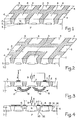
- Figure 1 partially and very schematically shows a portion of a conventional bipolar integrated circuit in perspective view and in section.
- This circuit is developed on a P-type substrate 1 on which is formed an N-type epitaxial layer divided into boxes by isolation walls 2 of P + type. Inside each of the boxes is formed a particular component, for example an NPN or PNP transistor, which is isolated from its neighbors by the isolation walls 2.
- a particular component for example an NPN or PNP transistor, which is isolated from its neighbors by the isolation walls 2.
- the polarity between the wells and the substrate linked to the supply voltage should be such that the NP junction between each well and the substrate is blocked.
- the substrate must be more negatively polarized than each of the wells.
- FIG. 2 In the prior art, in an attempt to resolve this problem of contamination of neighboring caissons of a caisson possibly subjected to different negative voltages, the structure schematically shown in Figures 2 and 3 has been adopted.
- an annular box 6 Around the caisson 3 capable of receiving voltages parasitic negative, an annular box 6 is provided which at least partially surrounds the box 3, and is interposed between the box 3 and the boxes 4 which it is desired to protect.
- a metallization 7 is deposited on the annular well 6, with the interposition, as is usual, of a layer 8 with a high doping level and of the same type of conductivity as that of the well 6 making it possible to ensure the ohmicity of the contact.
- This annular metallization 7 is connected to the positive supply terminal of the integrated circuit.
- an object of the present invention is to provide a new type of device for protection against leakage currents in an integrated circuit having better results than the means employed in the prior art.
- an object of the present invention is to provide such a protection device which does not cause power dissipation in the integrated circuit.
- Another object of the present invention is to provide a protection device reducing the leakage currents by a factor of 10 5 to 10 7 and not simply by 10 like the means of the prior art.
- the present invention provides, as was already known, to surround a box capable of being parasitized by an annular box.
- this annular box is connected to its corresponding external isolation wall.
- the isolation wall separating the parasitic box from the annular box is connected to the most negative potential of the supply voltage.
- the annular box no longer has the same function as that of the prior art and the protection of neighboring caissons of the caisson likely to be parasitized is ensured by the creation of an electric field opposing the diffusion of the electrons generated in the vicinity of the junction between the parasitized caisson and the substrate.
- Figure 4 shows a sectional view of a structure according to the present invention.
- This sectional view corresponds to the top view of FIG. 2, that is to say that the box 3, capable of receiving negative parasitic voltages, is surrounded by an annular box 6 to protect the neighboring boxes 4.
- the difference between the present invention as shown schematically in Figure 4 and the devices of the prior art as shown schematically in Figure 3 lies mainly in the metallizations and connections of the various layers.
- the isolation wall 20 separating the box 3 from the annular box 6 is covered with a metallization 21 connected to the most negative supply terminal of the circuit.
- An overdoped zone 22 of type P + is provided if necessary to improve the ohmicity of the contact between the metallization 21 and the surface of the insulation wall 20.
- the wall d is designated by the reference 30 insulation external to the annular box 6, the apparent surface of this isolation wall is connected by a metallization 31 to the apparent surface of the annular box 6.
- an overdoped layer 8 ensures the ohmicity of the contact between the box 6 and the metallization 31.
- an overdoped area 32 ensures, if necessary, the consistency of the contact between the metallization 31 and the surface of the insulation wall 30.
- Figure 5 substantially repeats Figure 4, but there is shown in addition the circulation of current lines and electric field so that this figure can serve as a support for the following theoretical presentation of the operation of the structure according to the present invention. This theoretical presentation is given only for explanatory purposes to help the reader better understand and generalize the present invention. However, any error or omission in this theoretical description cannot affect the validity of the present invention, the results of which have been observed experimentally by the applicant as will be explained below.
- the conduction current in the substrate resulting from majority carriers (holes) is shown in solid lines, and in dotted lines, the diffusion current of minority carriers (electrons), it being understood that the electrons propagate in the direction inverse of the direction designated by the arrows in the figure which corresponds to the conventional representation of current flow.
- the most negative potential of the power source has been represented by the conventional symbol of the mass.
- the current 41 results from current 40 and is substantially proportional to this current 40 or stray current.
- This current 41 generates in the substrate 1, which has a given resistivity, a radial electric field E oriented towards the outside of the box 3 and also having an intensity roughly proportional to the stray current 40 from which it results.
- the recombination current (not represented in FIG. 5) is supplied to the substrate by the metallization 21 and the wall 20.
- the parasitic current generating electrons in the substrate creates an electric field serving for the confinement of these electrons and produces its own remedy. A correction proportional to the magnitude of the current resulting from the parasitic voltages is thus obtained.
- the quality of this compensation will be illustrated in relation to the diagrams in Figures 6 and 7 below.
- the ordinates indicate the sum of the leakage currents I f in the caissons to be protected such as the caissons 4 of FIG. 2 while the abscissae indicate the parasitic current Ip injected into the parasitic well such as well 3 of FIG. 2.
- the abscissae are in mA and correspond to a variation of the current Ip from 0 to 50 mA and the ordinates are, for FIG. 6 in mA and extend in the range of 0 to 1 mA and for Figure 7 in ltA and extend in the range of 0 to 50, uA
- the curve 50 corresponds to the structures of the prior art as illustrated in FIG. 3 and the curve 51 corresponds to a structure according to the present invention as illustrated in FIGS. 4 and 5.
- FIG. 6 clearly shows that , for a structure according to the prior art, a leakage current of the order of mA is reached for all the transistors to be protected as soon as the injected current reaches a value of the order of 10 mA, that is to say that is to say that only 9/10 of the injected current is absorbed by the annular box.
- the structure according to the present invention makes it possible to obtain leakage currents in the wells 4 to be protected less than a few tens of ⁇ A in a range going from 0 to 30 mA for the injected current, this sum of the leakage currents being even less than the iiA for values of the injected current comprised between approximately 10 and 30 mA.
- Curve 51 is shown in FIG. 7 with a dilated scale on the ordinate.
- the metallization 31 (see FIG. 4) to a metallization integral with the substrate 1 and more particularly with the underside of this substrate.
- the curve 51 is then extended by the dotted curve designated by the reference 52 in FIG. 7 and the device retains all its effectiveness against injected currents which may be greater than 100 mA.
- the present invention has been explained previously in the case of a monolithic integrated circuit produced on a P-type substrate. If the bipolar integrated circuit was produced on an N-type substrate, all that has been said previously would remain valid by inverting all the types of conductivity as well as the directions of the currents. In particular, the reference voltage of the power source which was the most negative voltage in the example described above would be the most positive voltage.
- the metallizations 21 and 31 can be interrupted over a portion of their perimeter to allow passage to other connection metallizations directed towards the component included in the box 3, which avoids having to resort to metallization overlays.
- the isolation walls surrounding the boxes containing these components will be connected to the wall 30 and to the box 6 by appropriately extending the metallization 31; this results in further improved protection of these boxes.
- the present invention may be applied to all integrated circuits which, by their environment, are capable of receiving large parasitic overvoltages, in particular in industrial and automotive electronics.
Landscapes
- Engineering & Computer Science (AREA)
- Power Engineering (AREA)
- Microelectronics & Electronic Packaging (AREA)
- Physics & Mathematics (AREA)
- Condensed Matter Physics & Semiconductors (AREA)
- General Physics & Mathematics (AREA)
- Computer Hardware Design (AREA)
- Manufacturing & Machinery (AREA)
- Ceramic Engineering (AREA)
- Semiconductor Integrated Circuits (AREA)
- Bipolar Integrated Circuits (AREA)
Description
La présente invention concerne un dispositif de protection contre les courants de fuite dans les circuits intégrés monolithiques, ces courants de fuite étant provoqués par des surtensions parasites inverses.The present invention relates to a device for protection against leakage currents in monolithic integrated circuits, these leakage currents being caused by reverse parasitic overvoltages.
Dans la description qui suit, on se référera à des circuits intégrés bipolaires à substrat de type P et couche épitaxiée de type N. Bien entendu, la présente invention s'applique également au cas où les types de conductivité des diverses couches sont tous inversés.In the following description, reference will be made to bipolar integrated circuits with P-type substrate and N-type epitaxial layer. Of course, the present invention also applies to the case where the conductivity types of the various layers are all reversed.
La figure 1 représente de façon partielle et très schématique une portion d'un circuit intégré bipolaire classique en vue en perspective et en coupe. Ce circuit est élaboré sur un substrat 1 de type P sur lequel est formé une couche épitaxiée de type N divisée en caissons par des murs d'isolement 2 de type P+. A l'intérieur de chacun des caissons est formé un composant particulier, par exemple un transistor NPN ou PNP, qui se trouve isolé de ses voisins par les murs d'isolement 2. Bien entendu, pour que le fonctionnement des composants situés à l'intérieur de chacun des caissons soit indépendant de celui des composants voisins, il convient que la polarité entre les caissons et le substrat liée à la tension d'alimentation soit telle que la jonction NP entre chaque caisson et le substrat soit bloquée. Ainsi, le substrat doit être polarisé plus négativement que chacun des caissons. Néanmoins, en raison de l'environnement et des connexions externes des composants situés dans les caissons, il se peut que l'un d'eux, par exemple le caisson 3, reçoive des tensions parasites plus négatives que la tension de polarisation du substrat. Alors, la jonction NP entre ce caisson et le substrat se trouvera débloquée et des électrons pourront être injectés dans le substrat. Ces électrons seront susceptibles de diffuser dans le substrat et seront collectés par les caissons environnants, désignés collectivement par la référence 4, d'où il pourra résulter l'apparition de courants de fuite dans les composants situés dans ces caissons environnants 4. Bien entendu, ce seront les caissons les plus immédiatement voisins du caisson parasité qui seront les plus susceptibles d'être affectés. Dans la figure 1, on a également représenté des couches enterrées 5 de type N+ + au fond de chacun des caissons 3 et 4, comme cela est classique dans la technologie des circuits intégrés bipolaires. Une autre façon de considérer les courants de fuite apparaissant dans des caissons 4 voisins d'un caisson 3 soumis à des surtensions négatives consiste à dire que ces courant de fuite résultent de la circulation de courant entre émetteur et collecteurs d'un transistor latéral multicollecteurs dont l'émetteur est constitué par le caisson 3 éventuellement soumis à une surtension négative parasite, dont la base est constituée par le substrat 1, et dont les collecteurs sont constitués par les divers caissons 4.Figure 1 partially and very schematically shows a portion of a conventional bipolar integrated circuit in perspective view and in section. This circuit is developed on a P-
Dans l'art antérieur, pour tenter de résoudre ce problème de contamination des caissons voisins d'un caisson éventuellement soumis à différentes tensions négatives, on a adopté la structure schématiquement représentée en figures 2 et 3. Autour du caisson 3 susceptible de recevoir des tensions négatives parasites, est prévu un caisson annulaire 6 qui entoure au moins partiellement le caisson 3, et est interposé entre le caisson 3 et les caissons 4 que l'on veut protéger. Comme le montre la figure 3, une métallisation 7 est déposée sur le caisson annulaire 6, avec interposition, comme cela est usuel, d'une couche 8 à niveau de dopage élevé et de même type de conductivité que celui du caisson 6 permettant d'assurer l'ohmicité du contact. Cette métallisation annulaire 7 est connectée à la borne d'alimentation positive du circuit intégré. Ainsi, si une surtension parasite, représentée sous la forme d'une source de courant 9 tendant à faire sortir du courant du caisson 3, est appliquée, il en résulte une injection d'électrons dans le substrat. Cette injection d'électrons est désignée par la flèche de forte épaisseur 10. Les électrons 10 ont tendance à être collectés par le caisson 6 puis sont renvoyés par la métallisation 7 et la connexion associée vers l'alimentation positive. Si l'on s'intéresse non plus au sens de conduction des électrons mais à la direction classique de passage de courant, on peut dire qu'un courant circule depuis la borne d'alimentation positive à travers le caisson annulaire 6, le substrat 1 et le caisson 3 vers la source de courant 9. Par ce procédé, une grande partie des électrons diffusant dans le substrat 1 sont collectés par le caisson annulaire 6. Néanmoins, une faible partie de ces électrons symbolisés par la flèche de faible épaisseur 11 continue à diffuser dans le substrat vers les caissons environnants 4 dans lesquels un courant de fuite est créé. Dans la pratique, la demanderesse a observé que seulement 9/10e du courant de fuite total est absorbé par le caisson annulaire 6 et qu'il demeure encore sensiblement 1/10e du courant injecté par la source de courant 9 qui contribue à la fuite des caissons 4. D'autre part, le courant prélevé sur l'alimentation positive de la source d'alimentation du circuit intégré contribue à accroître la puissance dissipée dans celui-ci. Pour remédier à ce dernier inconvénient, il est également possible de relier la métallisation du caisson annulaire à la masse, ce qui réduit la puissance dissipée dans le circuit intégré mais réduit également l'efficacité de collection de ce caisson annulaire.In the prior art, in an attempt to resolve this problem of contamination of neighboring caissons of a caisson possibly subjected to different negative voltages, the structure schematically shown in Figures 2 and 3 has been adopted. Around the
Ainsi, un objet de la présente invention est de prévoir un nouveau type de dispositif de protection contre les courants de fuite dans un circuit intégré présentant de meilleurs résultats que les moyens employés dans l'art antérieur.Thus, an object of the present invention is to provide a new type of device for protection against leakage currents in an integrated circuit having better results than the means employed in the prior art.
Notamment, un objet de la présente invention est de prévoir un tel dispositif de protection n'entraînant pas de dissipation de puissance dans le circuit intégré.In particular, an object of the present invention is to provide such a protection device which does not cause power dissipation in the integrated circuit.
Un autre objet de la présente invention est de prévoir un dispositif de protection réduisant les courants de fuite d'un facteur de 105 à 107 et non pas simplement de 10 comme les moyens de l'art antérieur.Another object of the present invention is to provide a protection device reducing the leakage currents by a factor of 10 5 to 10 7 and not simply by 10 like the means of the prior art.
Pour atteindre ces objets ainsi que d'autres, la présente invention prévoit, comme cela était déjà connu, d'entourer un caisson susceptible d'être parasité d'un caisson annulaire. Mais, au lieu de relier ce caisson annulaire à la borne d'alimentation positive du circuit intégré, ce caisson annulaire est connecté à son mur d'isolement externe correspondant. D'autre part, le mur d'isolement séparant le caisson parasité du caisson annulaire est connecté au potential le plus négatif de la tension d'alimentation.To achieve these and other objects, the present invention provides, as was already known, to surround a box capable of being parasitized by an annular box. However, instead of connecting this annular box to the positive supply terminal of the integrated circuit, this annular box is connected to its corresponding external isolation wall. On the other hand, the isolation wall separating the parasitic box from the annular box is connected to the most negative potential of the supply voltage.
Comme on le verra dans la description détaillée ci-après de modes de réalisation particuliers de la présente invention, quand on réalise les connexions indiquées ci-dessus, le caisson annulaire n'a plus la même fonction que celui de l'art antérieur et la protection des caissons voisins du caisson susceptible d'être parasité est assurée par la création d'un champ électrique s'opposant à la diffusion des électrons engendrés au voisinage de la jonction entre le caisson parasité et le substrat.As will be seen in the detailed description below of particular embodiments of the present invention, when the connections indicated above are made, the annular box no longer has the same function as that of the prior art and the protection of neighboring caissons of the caisson likely to be parasitized is ensured by the creation of an electric field opposing the diffusion of the electrons generated in the vicinity of the junction between the parasitized caisson and the substrate.
Ces objets, caractéristiques et avantages ainsi que d'autres de la présente invention seront exposés plus en détail dans la description suivante de modes de réalisation particuliers, faite en relation avec les figures jointes parmi lesquelles:
- les figures 1 à 3 qui étaient destinées à poser le problème résolu par la présente invention et à exposer les solutions partielles de l'art antérieur ont été décrites précédemment;
- la figure 4 est une vue en coupe schématique illustrant la présente invention;
- la figure 5 est une vue en coupe schématique destinée à servir de support à un exposé théorique sur le fonctionnement de la structure selon la présente invention;
- les figures 6 et 7 sont des courbes illustrant les résultats obtenus par l'utilisation de la structure selon la présente invention.
- Figures 1 to 3 which were intended to pose the problem solved by the present invention and to expose the partial solutions of the prior art have been described above;
- Figure 4 is a schematic sectional view illustrating the present invention;
- Figure 5 is a schematic sectional view intended to serve as a support for a theoretical presentation on the operation of the structure according to the present invention;
- Figures 6 and 7 are curves illustrating the results obtained by the use of the structure according to the present invention.
Dans ces diverses figures, on notera que, conformément à l'usage dans le domaine des semiconducteurs, les diverses couches et zones semiconductrices ne sont pas représentées à l'échelle ni d'une figure à l'autre ni à l'intérieur d'une même figure mais sont uniquement tracées dans un but illustratif. D'autre part, dans les diverses figures, des références identiques désignent des zones, couches ou composants analogues.In these various figures, it will be noted that, in accordance with the practice in the field of semiconductors, the various layers and semiconductor zones are not shown to scale neither from one figure to another nor inside. the same figure but are only drawn for illustrative purposes. On the other hand, in the various figures, identical references designate zones, layers or similar components.
La figure 4 représente une vue en coupe d'une structure selon la présente invention. Cette vue en coupe correspond à la vue de dessus de la figure 2, c'est-à-dire gue le caisson 3, susceptible de recevoir des tensions parasites négatives est entouré d'un caisson annulaire 6 pour protéger les caissons voisins 4. La différence entre la présente invention telle qu'elle est représentée schématiquement en figure 4 et les dispositifs de l'art antérieur tels qu'ils sont schématiquement représentés en figure 3 réside essentiellement dans les métallisations et connexions des diverses couches. Selon la présente invention, le mur d'isolement 20 séparant le caisson 3 du caisson annulaire 6 est recouvert d'une métallisation 21 connectée à la borne d'alimentation la plus négative du circuit. Une zone surdopée 22 de type P+ est prévue si nécessaire pour améliorer l'ohmicité du contact entre la métallisation 21 et la surface du mur d'isolement 20. D'autre part, si l'on désigne par la référence 30 le mur d'isolement externe au caisson annulaire 6, la surface apparente de ce mur d'isolement est reliée par une métallisation 31 à la surface apparente du caisson annulaire 6. Comme dans le cas de la figure 3, une couche surdopée 8 assure l'ohmicité du contact entre le caisson 6 et la métallisation 31. De même, une zone surdopée 32 assure si nécessaire l'ohmicité du contact entre la métallisation 31 et la surface du mur d'isolement 30.Figure 4 shows a sectional view of a structure according to the present invention. This sectional view corresponds to the top view of FIG. 2, that is to say that the
La figure 5 reprend sensiblement la figure 4, mais on y a représenté en plus la circulation de lignes de courant et de champ électrique pour que cette figure puisse servir de support à l'exposé théorique suivant du fonctionnement de la structure selon la présente invention. Cet exposé théorique est donné uniquement à titre explicatif pour aider le lecteur à mieux comprendre et généraliser la présente invention. Néanmoins, toute erreur ou omission dans cet exposé théorique ne saurait affecter la validité de la présente invention dont les résultats ont été constatés expérimentalement par la demanderesse comme cela sera exposé ci-après.Figure 5 substantially repeats Figure 4, but there is shown in addition the circulation of current lines and electric field so that this figure can serve as a support for the following theoretical presentation of the operation of the structure according to the present invention. This theoretical presentation is given only for explanatory purposes to help the reader better understand and generalize the present invention. However, any error or omission in this theoretical description cannot affect the validity of the present invention, the results of which have been observed experimentally by the applicant as will be explained below.
Dans la figure, on a représenté en trait plein le courant de conduction dans le substrat résultant de porteurs majoritaires (trous), et en pointillé, le courant de diffusion des porteurs minoritaires (électrons), étant entendu que les électrons se propagent dans la direction inverse du sens désigné par les flèches sur la figure qui correspond à la représentation conventionelle de circulation du courant. Dans la figure 5, on a représenté par le symbole classique de la masse le potentiel le plus négatif de la source d'alimentation.In the figure, the conduction current in the substrate resulting from majority carriers (holes) is shown in solid lines, and in dotted lines, the diffusion current of minority carriers (electrons), it being understood that the electrons propagate in the direction inverse of the direction designated by the arrows in the figure which corresponds to the conventional representation of current flow. In FIG. 5, the most negative potential of the power source has been represented by the conventional symbol of the mass.
Quand une tension plus négative que le potentiel de référence, à savoir la masse dans l'exemple représenté, est appliquée sur le caissons 3, des électrons sont injectés en-dessous de ce caisson dans le substrat 1 et diffusent radialement comme indiqué par les traits en pointillé. Ces électrons sont collectés par le caisson annulaire 6 et le courant se referme vers la masse en passant par la métallisation 31, le mur 30, à nouveau le substrat 1, le mur 20 intermédiaire entre le caisson annulaire 6 et le caisson 3, et la métallisation 21. Il passe donc dans le substrat 1 deux courants en sens inverses: un courant 40 dirigé vers le caisson 3 et correspondant à la diffusion des électrons et un courant 41 dirigé vers l'extérieur par rapport au caisson 3 et correspondant à la conduction entre les murs 20 et 30. Il est important de noter que le courant 41 résulte du courant 40 et est sensiblement proportionnel à ce courant 40 ou courant parasite. Ce courant 41 engendre dans le substrat 1, qui a une résistivité donnée, un champ électrique E radial orienté vers l'extérieur du caisson 3 et ayant également une intensité à peu près proportionnelle au courant parasite 40 dont il résulte. Ainsi, les électrons en excès sous le caisson 3 ne peuvent pas traverser la barrière de potentiel établie par ce champ électrique E et se recombinent sur place. Le courant de recombinaison (non représenté en figure 5) est fourni au substrat par la métallisation 21 et le mur 20. En d'autres termes, le courant parasite générateur d'électrons dans le substrat crée un champ électrique servant au confinement de ces électrons et produit son propre remède. On obtient ainsi une correction proportionelle à l'importance du courant résultant des tensions parasites. La qualité de cette compensation va être illustrée en relation avec les diagrammes des figures 6 et 7 suivantes.When a voltage more negative than the reference potential, namely the mass in the example shown, is applied to the
Dans les figures 6 et 7, correspondant à des oscillogrammes relevés par l'inventeur, les ordonnées indiquent la somme des courants de fuite If dans les caissons à protéger tels que les caissons 4 de la figure 2 alors que les abscisses indiquent le courant parasite Ip injecté dans le caisson parasité tel que le caisson 3 de la figure 2. Les abscisses sont en mA et correspondent à une variation du courant Ip de 0 à 50 mA et les ordonnées sont, pour la figure 6 en mA et s'étendent dans la gamme de 0 à 1 mA et pour la figure 7 en ltA et s'étendent dans la gamme de 0 à 50 ,u.A.In FIGS. 6 and 7, corresponding to oscillograms noted by the inventor, the ordinates indicate the sum of the leakage currents I f in the caissons to be protected such as the
En figure 6, la courbe 50 correspond aux structures de l'art antérieur telles qu'illustrées en figure 3 et la courbe 51 correspond à une structure selon la présente invention telle qu'illustrée en figures 4 et 5. La figure 6 montre bien que, pour une structure selon l'art antérieur, on atteint un courant de fuite de l'ordre du mA pour l'ensemble des transistors à protéger dès que le courant injecté atteint une valeur de l'ordre de 10 mA, c'est-à-dire que seulement les 9/10e du courant injecté sont absorbés par le caisson annulaire. Par contre, comme le montre la courbe 51, la structure selon la présente invention permet d'obtenir des courants de fuite dans les caissons 4 à protéger inférieurs à quelques dizaines de µA dans une gamme allant de 0 à 30 mA pour le courant injecté, cette somme des courants de fuite étant même inférieure au iiA pour des valeurs du courant injecté comprises entre environ 10 et 30 mA.In FIG. 6, the
La courbe 51 est reprise en figure 7 avec une échelle dilatée en ordonnées. Pour éviter la croissance du courant (qui reste toutefois bien inférieure à celle des structures de l'art antérieur), pour des valeur injectées du courant parasite supérieures à 30 mA, c'est-à-dire pour de fortes tensions parasites négatives appliquées, il est prévu selon la présente invention de relier la métallisation 31 (voir figure 4) à une métallisation solidaire du substrat 1 et plus particulièrement de la face inférieure de ce substrat. La courbe 51, se prolonge alors par la courbe en pointillé désignée par la référence 52 en figure 7 et le dispositif conserve toute son efficacité contre des courants injectés pouvant être supérieurs à 100 mA. On peut estimer que la raison théorique de cette compensation est liée au fait que la croissance des courants de fuite pour des valeurs du courant injecté supérieures à 30 mA est liée à la chute de tension due à la résistance interposée entre la masse et la jonction entre le substrat 1 et le caisson 6. Cette résistance est égale à la somme de la résistance du substrat entre les murs d'isolement 20 et 30, de la résistance du mur 20, de celle du mur 30 et de celle du caisson 6. Si la chute de tension de cette résistance atteint un seuil de diode (environ 0,8 volt), la jonction substrat 1, caisson 6 devient polarisée dans le sens direct et injecte les électrons supplémentaires dans le substrat. La connexion indiquée plus haut entre la métallisation 31 et le substrat permet d'éviter cette injection.
La présente invention a été exposée précédemment dans le cas d'un circuit intégré monolithique élaboré sur un substrat de type P. Si le circuit intégré bipolaire était élaboré sur un substrat de type N, tout ce qui a été dit précédemment resterait valable en inversant tous les types de conductivité ainsi que les sens des courants. Notamment, la tension de référence de la source d'alimentation qui était la tension la plus négative dans l'exemple décrit précédemment serait la tension la plus positive.The present invention has been explained previously in the case of a monolithic integrated circuit produced on a P-type substrate. If the bipolar integrated circuit was produced on an N-type substrate, all that has been said previously would remain valid by inverting all the types of conductivity as well as the directions of the currents. In particular, the reference voltage of the power source which was the most negative voltage in the example described above would be the most positive voltage.
D'autre part, si le caisson 6 doit bien entourer complètement la caisson parasité, par contre les métallisations 21 et 31 peuvent être interrompues sur une portion de leur périmètre pour laisser le passage à d'autres métallisations de connexion dirigées vers le composant inclus dans le caisson 3, ce qui évite d'avoir recours à des superpositions de métallisation. En outre, si des composants situés dans certains caissons 4 sont particulièrement sensibles aux courants de fuite, en raison par exemple du courant très faible avec lequel ils doivent fonctionner, il est évidemment avantageux d'éloigner ces composants du caisson parasité, mais, de plus, selon une caractéristique de la présente invention, on reliera les murs d'isolement entourant les caissons contenant ces composants au mur 30 et au caisson 6 en prolongeant de façon appropriée la métallisation 31; il en résulte une protection encore améliorée de ces caissons.On the other hand, if the
La présente invention pourra s'appliquer à tous les circuits intégrés qui, de par leur environnement, sont susceptibles de recevoir des surtensions parasites importantes, notamment en électronique industrielle et automobile.The present invention may be applied to all integrated circuits which, by their environment, are capable of receiving large parasitic overvoltages, in particular in industrial and automotive electronics.
La présente invention n'est pas limitée aux exemples de réalisation décrits précédemment. Elle en comprend les diverses variantes et généralisations incluses dans le domaine des revendications ci-après.The present invention is not limited to examples of embodiments described above. It includes the various variants and generalizations thereof included in the field of claims below.
Claims (9)
Applications Claiming Priority (2)
| Application Number | Priority Date | Filing Date | Title |
|---|---|---|---|
| FR8010842 | 1980-05-14 | ||
| FR8010842A FR2492165A1 (en) | 1980-05-14 | 1980-05-14 | DEVICE FOR PROTECTION AGAINST LEAKAGE CURRENTS IN INTEGRATED CIRCUITS |
Publications (2)
| Publication Number | Publication Date |
|---|---|
| EP0040125A1 EP0040125A1 (en) | 1981-11-18 |
| EP0040125B1 true EP0040125B1 (en) | 1983-11-30 |
Family
ID=9241989
Family Applications (1)
| Application Number | Title | Priority Date | Filing Date |
|---|---|---|---|
| EP81400665A Expired EP0040125B1 (en) | 1980-05-14 | 1981-04-28 | Protection device against parasitic currents in integrated circuits |
Country Status (4)
| Country | Link |
|---|---|
| US (1) | US4466011A (en) |
| EP (1) | EP0040125B1 (en) |
| DE (1) | DE3161536D1 (en) |
| FR (1) | FR2492165A1 (en) |
Families Citing this family (28)
| Publication number | Priority date | Publication date | Assignee | Title |
|---|---|---|---|---|
| DE3276513D1 (en) * | 1982-11-26 | 1987-07-09 | Ibm | Self-biased resistor structure and application to interface circuits realization |
| IT1231894B (en) * | 1987-10-15 | 1992-01-15 | Sgs Microelettronica Spa | INTEGRATED DEVICE TO SCREEN THE INJECTION OF CHARGES INTO THE SUBSTRATE. |
| IT1232930B (en) * | 1987-10-30 | 1992-03-10 | Sgs Microelettronica Spa | INTEGRATED STRUCTURE WITH ACTIVE AND PASSIVE COMPONENTS INCLUDED IN INSULATION BAGS OPERATING AT A VOLTAGE GREATER THAN THE BREAKING VOLTAGE BETWEEN EACH COMPONENT AND THE BAG CONTAINING IT |
| FR2624320B1 (en) * | 1987-12-02 | 1990-05-18 | Equip Electr Moteur | MONOLITHIC REGULATOR OF BATTERY CHARGE VOLTAGE BY AN ALTERNATOR PROTECTED AGAINST INTERFERENCE VOLTAGES |
| DE3924278A1 (en) * | 1988-08-10 | 1990-02-15 | Bosch Gmbh Robert | ELECTRONIC, MONOLITHICALLY INTEGRATED DEVICE |
| IT1231541B (en) * | 1989-07-25 | 1991-12-17 | Sgs Thomson Microelectronics | PROTECTION DEVICE AGAINST PARASITIC EFFECTS CAUSED BY NEGATIVE POWER SUPPLY VOLTAGES IN INTEGRATED MONOLITHIC CIRCUITS INCLUDING A POWER DEVICE FOR THE PILOTING OF AN INDUCTIVE LOAD AND A CONTROL DEVICE FOR THAT POWER DEVICE. |
| IT1236797B (en) * | 1989-11-17 | 1993-04-02 | St Microelectronics Srl | VERTICAL-TYPE MONOLITHIC SEMICONDUCTOR POWER DEVICE WITH PROTECTION AGAINST PARASITE CURRENTS. |
| JPH03203265A (en) * | 1989-12-28 | 1991-09-04 | Sony Corp | Semiconductor device and manufacture thereof |
| WO1991016728A1 (en) * | 1990-04-13 | 1991-10-31 | Kabushiki Kaisha Toshiba | Substrate structure of a semiconductor device |
| US5148099A (en) * | 1991-04-01 | 1992-09-15 | Motorola, Inc. | Radiation hardened bandgap reference voltage generator and method |
| DE4133245C2 (en) * | 1991-10-08 | 2001-09-20 | Bosch Gmbh Robert | Bipolar monolithic integrated circuit |
| DE4209523C1 (en) * | 1992-03-24 | 1993-03-11 | Siemens Ag, 8000 Muenchen, De | |
| US5243214A (en) * | 1992-04-14 | 1993-09-07 | North American Philips Corp. | Power integrated circuit with latch-up prevention |
| JP3252569B2 (en) * | 1993-11-09 | 2002-02-04 | 株式会社デンソー | Insulating separation substrate, semiconductor device using the same, and method of manufacturing the same |
| US5514901A (en) * | 1994-05-17 | 1996-05-07 | Allegro Microsystems, Inc. | Epitaxial island with adjacent asymmetrical structure to reduce collection of injected current from the island into other islands |
| US5545917A (en) * | 1994-05-17 | 1996-08-13 | Allegro Microsystems, Inc. | Separate protective transistor |
| US5834826A (en) * | 1997-05-08 | 1998-11-10 | Stmicroelectronics, Inc. | Protection against adverse parasitic effects in junction-isolated integrated circuits |
| US6737713B2 (en) * | 2001-07-03 | 2004-05-18 | Tripath Technology, Inc. | Substrate connection in an integrated power circuit |
| JP2003229502A (en) * | 2002-02-01 | 2003-08-15 | Mitsubishi Electric Corp | Semiconductor device |
| US20040053439A1 (en) * | 2002-09-17 | 2004-03-18 | Infineon Technologies North America Corp. | Method for producing low-resistance ohmic contacts between substrates and wells in CMOS integrated circuits |
| US6747294B1 (en) | 2002-09-25 | 2004-06-08 | Polarfab Llc | Guard ring structure for reducing crosstalk and latch-up in integrated circuits |
| DE10314151B4 (en) * | 2003-03-28 | 2008-04-24 | Infineon Technologies Ag | Semiconductor device arrangement and method for compensation of parasitic currents |
| CA2533225C (en) | 2006-01-19 | 2016-03-22 | Technologies Ltrim Inc. | A tunable semiconductor component provided with a current barrier |
| US7514754B2 (en) * | 2007-01-19 | 2009-04-07 | Episil Technologies Inc. | Complementary metal-oxide-semiconductor transistor for avoiding a latch-up problem |
| US7411271B1 (en) * | 2007-01-19 | 2008-08-12 | Episil Technologies Inc. | Complementary metal-oxide-semiconductor field effect transistor |
| US7538396B2 (en) * | 2007-01-19 | 2009-05-26 | Episil Technologies Inc. | Semiconductor device and complementary metal-oxide-semiconductor field effect transistor |
| US7700405B2 (en) * | 2007-02-28 | 2010-04-20 | Freescale Semiconductor, Inc. | Microelectronic assembly with improved isolation voltage performance and a method for forming the same |
| US9478607B2 (en) | 2014-09-11 | 2016-10-25 | Semiconductor Components Industries, Llc | Electronic device including an isolation structure |
Citations (4)
| Publication number | Priority date | Publication date | Assignee | Title |
|---|---|---|---|---|
| FR1510057A (en) | 1966-12-06 | 1968-01-19 | Csf | Complementary integrated npn and pnp transistors with isolated collectors |
| CH506889A (en) | 1970-07-24 | 1971-04-30 | Foerderung Forschung Gmbh | Integrated circuit |
| FR2113906A1 (en) | 1970-11-12 | 1972-06-30 | Itt | |
| FR2303382A1 (en) | 1975-03-07 | 1976-10-01 | Nat Semiconductor Corp | Monolithic integrated semiconductor circuit - uses electron flux reduction from substrate to epitaxial tank resulting in current flow reduction |
Family Cites Families (7)
| Publication number | Priority date | Publication date | Assignee | Title |
|---|---|---|---|---|
| US4044373A (en) * | 1967-11-13 | 1977-08-23 | Hitachi, Ltd. | IGFET with gate protection diode and antiparasitic isolation means |
| NL161923C (en) * | 1969-04-18 | 1980-03-17 | Philips Nv | SEMICONDUCTOR DEVICE. |
| US3590345A (en) * | 1969-06-25 | 1971-06-29 | Westinghouse Electric Corp | Double wall pn junction isolation for monolithic integrated circuit components |
| US3878551A (en) * | 1971-11-30 | 1975-04-15 | Texas Instruments Inc | Semiconductor integrated circuits having improved electrical isolation characteristics |
| US3931634A (en) * | 1973-06-14 | 1976-01-06 | Rca Corporation | Junction-isolated monolithic integrated circuit device with means for preventing parasitic transistor action |
| US3940785A (en) * | 1974-05-06 | 1976-02-24 | Sprague Electric Company | Semiconductor I.C. with protection against reversed power supply |
| US4027325A (en) * | 1975-01-30 | 1977-05-31 | Sprague Electric Company | Integrated full wave diode bridge rectifier |
-
1980
- 1980-05-14 FR FR8010842A patent/FR2492165A1/en active Granted
-
1981
- 1981-04-28 DE DE8181400665T patent/DE3161536D1/en not_active Expired
- 1981-04-28 EP EP81400665A patent/EP0040125B1/en not_active Expired
- 1981-05-13 US US06/263,203 patent/US4466011A/en not_active Expired - Lifetime
Patent Citations (4)
| Publication number | Priority date | Publication date | Assignee | Title |
|---|---|---|---|---|
| FR1510057A (en) | 1966-12-06 | 1968-01-19 | Csf | Complementary integrated npn and pnp transistors with isolated collectors |
| CH506889A (en) | 1970-07-24 | 1971-04-30 | Foerderung Forschung Gmbh | Integrated circuit |
| FR2113906A1 (en) | 1970-11-12 | 1972-06-30 | Itt | |
| FR2303382A1 (en) | 1975-03-07 | 1976-10-01 | Nat Semiconductor Corp | Monolithic integrated semiconductor circuit - uses electron flux reduction from substrate to epitaxial tank resulting in current flow reduction |
Also Published As
| Publication number | Publication date |
|---|---|
| US4466011A (en) | 1984-08-14 |
| DE3161536D1 (en) | 1984-01-05 |
| EP0040125A1 (en) | 1981-11-18 |
| FR2492165B1 (en) | 1984-05-04 |
| FR2492165A1 (en) | 1982-04-16 |
Similar Documents
| Publication | Publication Date | Title |
|---|---|---|
| EP0040125B1 (en) | Protection device against parasitic currents in integrated circuits | |
| EP0357528B1 (en) | Mos transistor and its use in a free running diode | |
| EP0721218B1 (en) | Power integrated circuit | |
| FR2812972A1 (en) | Semiconductor device e.g. silicon controlled rectifier has P+ and N+ regions formed respectively in N-type well region, which are connected to external pad | |
| FR2503456A1 (en) | PROTECTIVE DEVICE FOR INTEGRATED CIRCUITS | |
| EP0576375A1 (en) | Diode structure for pad protection | |
| WO1999035692A1 (en) | Subscriber interface protection circuit | |
| EP0614232B1 (en) | Reference diode in bipolar integrated circuit | |
| EP0543745B1 (en) | MOS transistor with integrated zener diode protection | |
| EP0581625A1 (en) | Multifunctional electronic device, in particular element with a negative dynamic resistance and corresponding method of fabrication | |
| FR2739224A1 (en) | BASE RESISTANCE CONTROLLED THYRISTOR STRUCTURE HAVING HIGH DENSITY IMPLANTATION FOR INCREASED CURRENT CAPACITY | |
| FR3091024A1 (en) | Single photon avalanche photodiode | |
| EP0521802B1 (en) | Avalanche diode in a bipolar integrated circuit | |
| EP3276662B1 (en) | Structure for protecting an integrated circuit against electrostatic discharges | |
| EP0090686B1 (en) | High current pnp transistor being part of a monolithic integrated circuit | |
| EP1076365A1 (en) | Sensitive static bidirectional switch | |
| FR2503933A1 (en) | INTEGRATED CIRCUIT COMPRISING A NETWORK OF TRANSISTORS | |
| FR2960342A1 (en) | HF CONTROL BIDIRECTIONAL SWITCH | |
| EP0462029B1 (en) | Process of fabricating a bipolar transistor sustaining a reverse bias | |
| EP0881672A1 (en) | Isolation wall between power device | |
| EP0886316A1 (en) | Protection of a logic device well comprising an integrated power MOS transistor | |
| FR2982077A1 (en) | TRIAC WITH TRIGGER AMPLIFICATION | |
| FR2693035A1 (en) | Protective diode for vertical semiconductor component. | |
| FR2495378A1 (en) | PROTECTION CIRCUIT, AGAINST TRANSIENT VOLTAGES, COMPRISING A THYRISTOR (SCR), FOR INTEGRATED CIRCUITS | |
| FR2783353A1 (en) | INSULATION WALL BETWEEN POWER COMPONENTS |
Legal Events
| Date | Code | Title | Description |
|---|---|---|---|
| PUAI | Public reference made under article 153(3) epc to a published international application that has entered the european phase |
Free format text: ORIGINAL CODE: 0009012 |
|
| AK | Designated contracting states |
Designated state(s): DE FR GB IT NL |
|
| 17P | Request for examination filed |
Effective date: 19811128 |
|
| ITF | It: translation for a ep patent filed | ||
| GRAA | (expected) grant |
Free format text: ORIGINAL CODE: 0009210 |
|
| AK | Designated contracting states |
Designated state(s): DE FR GB IT NL |
|
| REF | Corresponds to: |
Ref document number: 3161536 Country of ref document: DE Date of ref document: 19840105 |
|
| PLBI | Opposition filed |
Free format text: ORIGINAL CODE: 0009260 |
|
| 26 | Opposition filed |
Opponent name: DEUTSCHE ITT INDUSTRIES GMBH Effective date: 19840809 |
|
| PLBN | Opposition rejected |
Free format text: ORIGINAL CODE: 0009273 |
|
| STAA | Information on the status of an ep patent application or granted ep patent |
Free format text: STATUS: OPPOSITION REJECTED |
|
| 27O | Opposition rejected |
Effective date: 19851011 |
|
| NLR2 | Nl: decision of opposition | ||
| PGFP | Annual fee paid to national office [announced via postgrant information from national office to epo] |
Ref country code: NL Payment date: 19900430 Year of fee payment: 10 |
|
| ITTA | It: last paid annual fee | ||
| PG25 | Lapsed in a contracting state [announced via postgrant information from national office to epo] |
Ref country code: NL Effective date: 19911101 |
|
| NLV4 | Nl: lapsed or anulled due to non-payment of the annual fee | ||
| REG | Reference to a national code |
Ref country code: FR Ref legal event code: D6 |
|
| PGFP | Annual fee paid to national office [announced via postgrant information from national office to epo] |
Ref country code: FR Payment date: 20000411 Year of fee payment: 20 |
|
| PGFP | Annual fee paid to national office [announced via postgrant information from national office to epo] |
Ref country code: GB Payment date: 20000426 Year of fee payment: 20 |
|
| PGFP | Annual fee paid to national office [announced via postgrant information from national office to epo] |
Ref country code: DE Payment date: 20000427 Year of fee payment: 20 |
|
| PG25 | Lapsed in a contracting state [announced via postgrant information from national office to epo] |
Ref country code: GB Free format text: LAPSE BECAUSE OF EXPIRATION OF PROTECTION Effective date: 20010427 |
|
| REG | Reference to a national code |
Ref country code: GB Ref legal event code: PE20 Effective date: 20010427 |