EP2325893A2 - Low voltage bidirectional protection diode - Google Patents
Low voltage bidirectional protection diode Download PDFInfo
- Publication number
- EP2325893A2 EP2325893A2 EP10189069A EP10189069A EP2325893A2 EP 2325893 A2 EP2325893 A2 EP 2325893A2 EP 10189069 A EP10189069 A EP 10189069A EP 10189069 A EP10189069 A EP 10189069A EP 2325893 A2 EP2325893 A2 EP 2325893A2
- Authority
- EP
- European Patent Office
- Prior art keywords
- regions
- type
- region
- forming
- protection diode
- Prior art date
- Legal status (The legal status is an assumption and is not a legal conclusion. Google has not performed a legal analysis and makes no representation as to the accuracy of the status listed.)
- Granted
Links
- 230000002457 bidirectional effect Effects 0.000 title claims abstract description 17
- 239000000758 substrate Substances 0.000 claims abstract description 15
- 238000002513 implantation Methods 0.000 claims abstract description 10
- 238000004519 manufacturing process Methods 0.000 claims abstract description 8
- 238000000034 method Methods 0.000 claims abstract description 5
- 238000002955 isolation Methods 0.000 claims description 3
- 238000009413 insulation Methods 0.000 abstract 1
- 230000015556 catabolic process Effects 0.000 description 7
- 238000001465 metallisation Methods 0.000 description 5
- 239000002019 doping agent Substances 0.000 description 4
- ZOXJGFHDIHLPTG-UHFFFAOYSA-N Boron Chemical compound [B] ZOXJGFHDIHLPTG-UHFFFAOYSA-N 0.000 description 2
- 229910052796 boron Inorganic materials 0.000 description 2
- 238000000407 epitaxy Methods 0.000 description 2
- 230000002093 peripheral effect Effects 0.000 description 2
- 238000000137 annealing Methods 0.000 description 1
- 229910052785 arsenic Inorganic materials 0.000 description 1
- RQNWIZPPADIBDY-UHFFFAOYSA-N arsenic atom Chemical compound [As] RQNWIZPPADIBDY-UHFFFAOYSA-N 0.000 description 1
- 230000015572 biosynthetic process Effects 0.000 description 1
- 230000007547 defect Effects 0.000 description 1
- 238000000227 grinding Methods 0.000 description 1
- 238000005468 ion implantation Methods 0.000 description 1
- 238000012986 modification Methods 0.000 description 1
- 230000004048 modification Effects 0.000 description 1
- 230000010287 polarization Effects 0.000 description 1
- 229910021420 polycrystalline silicon Inorganic materials 0.000 description 1
- 230000001681 protective effect Effects 0.000 description 1
Images

Classifications
-
- H—ELECTRICITY
- H01—ELECTRIC ELEMENTS
- H01L—SEMICONDUCTOR DEVICES NOT COVERED BY CLASS H10
- H01L29/00—Semiconductor devices adapted for rectifying, amplifying, oscillating or switching, or capacitors or resistors with at least one potential-jump barrier or surface barrier, e.g. PN junction depletion layer or carrier concentration layer; Details of semiconductor bodies or of electrodes thereof ; Multistep manufacturing processes therefor
- H01L29/66—Types of semiconductor device ; Multistep manufacturing processes therefor
- H01L29/86—Types of semiconductor device ; Multistep manufacturing processes therefor controllable only by variation of the electric current supplied, or only the electric potential applied, to one or more of the electrodes carrying the current to be rectified, amplified, oscillated or switched
- H01L29/861—Diodes
- H01L29/8618—Diodes with bulk potential barrier, e.g. Camel diodes, Planar Doped Barrier diodes, Graded bandgap diodes
-
- H—ELECTRICITY
- H01—ELECTRIC ELEMENTS
- H01L—SEMICONDUCTOR DEVICES NOT COVERED BY CLASS H10
- H01L29/00—Semiconductor devices adapted for rectifying, amplifying, oscillating or switching, or capacitors or resistors with at least one potential-jump barrier or surface barrier, e.g. PN junction depletion layer or carrier concentration layer; Details of semiconductor bodies or of electrodes thereof ; Multistep manufacturing processes therefor
- H01L29/66—Types of semiconductor device ; Multistep manufacturing processes therefor
- H01L29/66007—Multistep manufacturing processes
- H01L29/66075—Multistep manufacturing processes of devices having semiconductor bodies comprising group 14 or group 13/15 materials
- H01L29/66083—Multistep manufacturing processes of devices having semiconductor bodies comprising group 14 or group 13/15 materials the devices being controllable only by variation of the electric current supplied or the electric potential applied, to one or more of the electrodes carrying the current to be rectified, amplified, oscillated or switched, e.g. two-terminal devices
- H01L29/6609—Diodes
- H01L29/66098—Breakdown diodes
- H01L29/66106—Zener diodes
-
- H—ELECTRICITY
- H01—ELECTRIC ELEMENTS
- H01L—SEMICONDUCTOR DEVICES NOT COVERED BY CLASS H10
- H01L29/00—Semiconductor devices adapted for rectifying, amplifying, oscillating or switching, or capacitors or resistors with at least one potential-jump barrier or surface barrier, e.g. PN junction depletion layer or carrier concentration layer; Details of semiconductor bodies or of electrodes thereof ; Multistep manufacturing processes therefor
- H01L29/66—Types of semiconductor device ; Multistep manufacturing processes therefor
- H01L29/86—Types of semiconductor device ; Multistep manufacturing processes therefor controllable only by variation of the electric current supplied, or only the electric potential applied, to one or more of the electrodes carrying the current to be rectified, amplified, oscillated or switched
- H01L29/861—Diodes
- H01L29/866—Zener diodes
Definitions
- the present invention relates to a low-voltage bidirectional protection diode, that is to say whose breakdown voltage in both directions is less than 10 volts, preferably close to 6 volts.
- bidirectional protection diodes encounter limitations when it is desired to reduce the breakdown voltage and more particularly when it is desired to obtain a symmetrical diode, that is to say having breakdown voltages. substantially equal and close to 6 to 10 volts.
- the known bidirectional diodes generally have a phenomenon of "snapback" according to at least one or the other of the two polarities, that is to say that, even if the voltage at which the breakdown is established is low, for example close to 10 volts, there is a short initial overvoltage, that is to say that the voltage across the diode rises to a value higher than the set value, for example to a value of 12 to 14 volts before falling to the protection value close to 10 volts.
- a general object of an embodiment of the present invention is to overcome at least some of the disadvantages of known bidirectional protection diodes.
- Another object of an embodiment of the present invention is to provide a bidirectional protection diode whose breakdown voltages are close to 6 volts in both directions.
- Another object of an embodiment of the present invention is to provide a bidirectional protection diode free of "snapback" phenomenon.
- Another object of an embodiment of the present invention is to provide a small bidirectional protection diode.
- an embodiment of the present invention provides a vertical bidirectional protection diode comprising, on a heavily doped substrate of a first conductivity type, first, second, and third regions of the first, second, and second regions. and first types of conductivity, these regions all having a doping level greater than 2 to 5x10 19 atoms per cm 3 and being delimited laterally by an isolated trench, each of these regions having a thickness of less than 4 ⁇ m.
- the second and third regions result from implantations in epitaxial layers with a thickness of less than 4 ⁇ m.
- the different regions are respectively of the P, N and P type, the first region having a maximum doping level of the order of 5 ⁇ 10 19 atoms per cm 3 , the second region having a level of maximum doping of the order of 10 20 atoms per cm 3 and the third region having a maximum doping level of the order of 5 ⁇ 10 19 atoms per cm 3 , the peaks of the doping curves of each of the regions being distant from less than of 3 ⁇ m.
- the last two steps are reversed.
- the various implantations are carried out at doses of between 1 and 10 ⁇ 10 16 atoms / cm 2 .
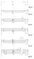
- the figure 1 represents a vertical-type diode comprising, above a P + type substrate 1, successive layers 3, 4 and 5 which are very strongly doped, respectively of P ++ , N ++ and P ++ type .
- the term "highly doped” refers to doping levels greater than or equal to 5 ⁇ 10 19 atoms / cm 3 .
- the underside of the substrate 1 is coated with a metallization M1.
- the set of layers 3, 4, 5 is delimited laterally by a peripheral trench 7 with insulated edges 8 and the upper layer 5 is coated with a metallization M2. Thanks to the very high doping levels of the N + base of the PNP transistor, the gain of this transistor is very low which eliminates the phenomenon of "snapback".
- the structure has a substantially symmetrical appearance.
- the fact that the active structure is surrounded by an isolated trench makes it possible to avoid any junction edge and curvature phenomena that would occur at the limits of the component in other types of structure.
- the figure 2 represents an example of doping levels chosen for the structure of the figure 1 .
- This figure 2 represents the concentration c in atoms / cm 3 as a function of the thickness e in micrometers.
- the thicknesses e3, e4 and e5 of the regions 3, 4 and 5 have been indicated.
- the thickness e4 of the N ++ layer 4 is preferably of the order of 2 ⁇ m. In practice, it will be in a range of 1.5 to 3 microns.
- the distance between each of the junctions and the maximum doping region of each of the P ++ regions 3 and 5 is of the order of 2 ⁇ m, and preferably in a range of 1 to 3 ⁇ m.
- Substrate 1 has been indicated as having a doping concentration of between 1 and 2 x 10 19 atoms / cm 3 . Indeed, it is the maximum limit of doping commercially available substrates. Of course, if we could supply substrates of higher doping level, the P ++ 3 layer could be useless.
- the Figures 3A to 3F illustrate successive steps of an exemplary method of manufacturing the bidirectional protection diode of the figure 1 .
- FIG. 3A As illustrated by figure 3A starting from a substrate P + 1 which is as doped as possible, for example from a doping level of 1 to 2 ⁇ 10 19 atoms / cm 3 , which corresponds to a resistance of 5 m ⁇ .cm.
- a P-type dopant is implanted, for example boron at shallow depth at the maximum possible dose, for example 1 to 10 ⁇ 10 16 atoms / cm 2 , to reach at the end of the process over a thickness of about 2 ⁇ m, a maximum doping level of the order of 5x10 19 atoms / cm 3 .
- Zone 3 is preferably localized, that is to say does not extend over the entire surface of the substrate, its implantation being limited by a mask.
- a localized implantation, above region 3, of an N-type dopant, for example arsenic, is carried out, for example at a dose of 1 to 10 ⁇ 10 16 atoms / cm 2 , for to reach, on the small thickness of the layer, a maximum concentration of the order of 2 ⁇ 10 20 atoms / cm 3 .
- a strong implantation of a P-type dopant for example boron
- a mask for example at a dose of 1 to 10 ⁇ 10.
- atoms / cm 2 to reach in this layer a maximum doping level of the order of 10 20 atoms / cm 3 .
- the structure is delimited by a peripheral trench 7.
- the origin of the thicknesses corresponds to the surface of the substrate 1, the negative thicknesses corresponding to the epitaxial layers.
- the present invention is susceptible of various variants.
- the stages of Figures 3E and 3F can be reversed, namely that isolation trenches can be carried out before carrying out the strong formation implantation of the P ++ 5 region.
- An advantage of the manufacturing method of the present invention is that the implantations are made at low energy in thin layers, which makes it possible to limit the creation of defects and to limit the annealing steps which would disturb the structure.
- this diode has between the metallizations M2 and M1 a breakdown voltage of the order of 6 volts in the two directions of polarization.
- the breakdown voltage can be adjusted to higher values, for example up to 10 V, by modifying the ion implantation doses for the production of layers 3, 4 and 5. The tests carried out show that no snapback phenomenon occurs.
Abstract
Description
La présente invention concerne une diode de protection bidirectionnelle basse tension, c'est-à-dire dont la tension de claquage dans les deux sens est inférieure à 10 volts, de préférence voisine de 6 volts.The present invention relates to a low-voltage bidirectional protection diode, that is to say whose breakdown voltage in both directions is less than 10 volts, preferably close to 6 volts.
De façon générale, les diverses techniques pour construire des diodes de protection bidirectionnelles se heurtent à des limitations quand on veut réduire la tension de claquage et plus particulièrement quand on veut obtenir une diode symétrique, c'est-à-dire présentant des tensions de claquage sensiblement égales et voisines de 6 à 10 volts. En plus, les diodes bidirectionnelles connues présentent généralement un phénomène de "snapback" selon au moins l'une ou l'autre des deux polarités, c'est-à-dire que, même si la tension à laquelle s'établit le claquage est faible, par exemple voisine de 10 volts, il se présente une brève surtension initiale, c'est-à-dire que la tension aux bornes de la diode monte à une valeur plus élevée que la valeur de consigne, par exemple à une valeur de 12 à 14 volts avant de chuter à la valeur de protection voisine de 10 volts.In general, the various techniques for constructing bidirectional protection diodes encounter limitations when it is desired to reduce the breakdown voltage and more particularly when it is desired to obtain a symmetrical diode, that is to say having breakdown voltages. substantially equal and close to 6 to 10 volts. In addition, the known bidirectional diodes generally have a phenomenon of "snapback" according to at least one or the other of the two polarities, that is to say that, even if the voltage at which the breakdown is established is low, for example close to 10 volts, there is a short initial overvoltage, that is to say that the voltage across the diode rises to a value higher than the set value, for example to a value of 12 to 14 volts before falling to the protection value close to 10 volts.
Ainsi, un objet général d'un mode de réalisation de la présente invention est de pallier au moins certains des inconvénients des diodes de protection bidirectionnelles connues.Thus, a general object of an embodiment of the present invention is to overcome at least some of the disadvantages of known bidirectional protection diodes.
Un autre objet d'un mode de réalisation de la présente invention est de prévoir une diode de protection bidirectionnelle dont les tensions de claquage sont voisines de 6 volts dans les deux directions.Another object of an embodiment of the present invention is to provide a bidirectional protection diode whose breakdown voltages are close to 6 volts in both directions.
Un autre objet d'un mode de réalisation de la présente invention est de prévoir une diode de protection bidirectionnelle exempte de phénomène de "snapback".Another object of an embodiment of the present invention is to provide a bidirectional protection diode free of "snapback" phenomenon.
Un autre objet d'un mode de réalisation de la présente invention est de prévoir une diode de protection bidirectionnelle de petite dimension.Another object of an embodiment of the present invention is to provide a small bidirectional protection diode.
Pour atteindre au moins certains de ces objets, un mode de réalisation de la présente invention prévoit une diode de protection bidirectionnelle verticale comprenant, sur un substrat fortement dopé d'un premier type de conductivité, des première, deuxième et troisième régions des premier, deuxième et premier types de conductivité, ces régions ayant toutes un niveau de dopage supérieur à 2 à 5x10¹⁹ atomes par cm3 et étant délimitées latéralement par une tranchée isolée, chacune des ces régions ayant une épaisseur inférieure à 4 µm.To achieve at least some of these objects, an embodiment of the present invention provides a vertical bidirectional protection diode comprising, on a heavily doped substrate of a first conductivity type, first, second, and third regions of the first, second, and second regions. and first types of conductivity, these regions all having a doping level greater than 2 to 5x10 19 atoms per cm 3 and being delimited laterally by an isolated trench, each of these regions having a thickness of less than 4 μm.
Selon un mode de réalisation de la présente invention, les deuxième et troisième régions résultent d'implantations dans des couches épitaxiées d'une épaisseur inférieure à 4 µm.According to one embodiment of the present invention, the second and third regions result from implantations in epitaxial layers with a thickness of less than 4 μm.
Selon un mode de réalisation de la présente invention, les différentes régions sont respectivement de type P, N et P, la première région ayant un niveau de dopage maximum de l'ordre de 5x10¹⁹ atomes par cm3, la deuxième région ayant un niveau de dopage maximum de l'ordre de 1020 atomes par cm3 et la troisième région ayant un niveau de dopage maximum de l'ordre de 5x10¹⁹ atomes par cm3, les sommets des courbes de dopage de chacune des régions étant distants de moins de 3 µm.According to one embodiment of the present invention, the different regions are respectively of the P, N and P type, the first region having a maximum doping level of the order of 5 × 10 19 atoms per cm 3 , the second region having a level of maximum doping of the order of 10 20 atoms per cm 3 and the third region having a maximum doping level of the order of 5 × 10 19 atoms per cm 3 , the peaks of the doping curves of each of the regions being distant from less than of 3 μm.
Un mode de réalisation de la présente invention prévoit un procédé de fabrication d'une diode de protection bidirectionnelle verticale comprenant les étapes suivante :
- former dans un substrat fortement dopé de type P, une première région très fortement dopée de type P ;
- former une première couche épitaxiée sur la structure ;
- former une deuxième région fortement dopée de type N dans la première couche épitaxiée ;
- former une deuxième couche épitaxiée sur la structure ;
- former une troisième région fortement dopée de type P dans la deuxième couche épitaxiée ;
- entourer la structure d'une tranchée d'isolement traversant les trois susdites régions.
- forming in a heavily doped P-type substrate a first very heavily doped P-type region;
- forming a first epitaxial layer on the structure;
- forming a second heavily doped N-type region in the first epitaxial layer;
- forming a second epitaxial layer on the structure;
- forming a third heavily doped P-type region in the second epitaxial layer;
- surround the structure of an isolation trench crossing the three aforesaid regions.
Selon un mode de réalisation de la présente invention, les deux dernières étapes sont inversées.According to an embodiment of the present invention, the last two steps are reversed.
Selon un mode de réalisation de la présente invention, les diverses implantations sont réalisées à des doses comprises entre 1 et 10x1016 atomes/cm2.According to one embodiment of the present invention, the various implantations are carried out at doses of between 1 and 10 × 10 16 atoms / cm 2 .
Ces objets, caractéristiques et avantages, ainsi que d'autres seront exposés en détail dans la description suivante de modes de réalisation particuliers faite à titre non-limitatif en relation avec les figures jointes parmi lesquelles :
- la
figure 1 est une vue en coupe illustrant une diode de protection selon un mode de réalisation de la présente invention ; - la
figure 2 représente des niveaux de dopage d'un exemple de la diode de lafigure 1 ; et - les
figures 3A à 3F représentent des étapes successives de fabrication d'une diode de protection bidirectionnelle selon un mode de réalisation de la présente invention.
- the
figure 1 is a sectional view illustrating a protective diode according to an embodiment of the present invention; - the
figure 2 represents doping levels of an example of the diode of thefigure 1 ; and - the
Figures 3A to 3F represent successive steps of manufacturing a bidirectional protection diode according to an embodiment of the present invention.
Comme cela est usuel dans le domaine de la représentation des microcomposants, les diverses vues en coupe ne sont pas tracées à l'échelle et sont seulement illustratives.As is customary in the field of representation of microcomponents, the various sectional views are not drawn to scale and are only illustrative.
La
La
On a indiqué le substrat 1 comme ayant une concentration de dopage comprise entre 1 et 2x10¹⁹ atomes/cm3. En effet, c'est la limite maximum de dopage des substrats commercialement disponibles. Bien entendu, si on pouvait approvisionner des substrats de plus fort niveau de dopage, la couche P++ 3 pourrait être inutile.
Les
Comme l'illustre la
Sur le substrat, on réalise une implantation d'un dopant de type P, par exemple du bore à faible profondeur à la dose maximale possible, par exemple 1 à 10x1016 atomes/cm2, pour atteindre en fin de processus sur une épaisseur d'environ 2 µm, un niveau de dopage maximum de l'ordre de 5x10¹⁹ atomes/cm3 . De préférence, la zone 3 est localisée, c'est-à-dire ne s'étend pas sur toute la surface du substrat, son implantation étant limitée par un masque.On the substrate, a P-type dopant is implanted, for example boron at shallow depth at the maximum possible dose, for example 1 to 10 × 10 16 atoms / cm 2 , to reach at the end of the process over a thickness of about 2 μm, a maximum doping level of the order of 5x10 19 atoms / cm 3 .
Comme l'illustre la
Comme l'illustre la
Comme l'illustre la
Comme l'illustre la
A l'étape illustrée en
On procède alors aux étapes classiques d'isolation des parois de la tranchée, de remplissage de la tranchée par exemple par du silicium polycristallin, éventuellement oxydé, de formation de la métallisation de face avant M1, de meulage de la face arrière du substrat pour obtenir une épaisseur de l'ordre de 50 à 200 µm pour la structure, puis de formation de la métallisation de face arrière M2 pour arriver au composant illustré en
On notera que dans la courbe de la
La présente invention est susceptible de diverses variantes. Par exemple, les étapes des
Un avantage du procédé de fabrication de la présente invention est que les implantations sont réalisées à faible énergie dans des couches peu épaisses, ce qui permet de limiter la création de défauts et de limiter les étapes de recuit qui perturberaient la structure.An advantage of the manufacturing method of the present invention is that the implantations are made at low energy in thin layers, which makes it possible to limit the creation of defects and to limit the annealing steps which would disturb the structure.
On constate que cette diode présente entre les métallisations M2 et M1 une tension de claquage de l'ordre de 6 volts dans les deux sens de polarisation. La tension de claquage peut être ajustée à des valeurs supérieures, par exemple jusqu'à 10 V, en modifiant les doses d'implantation ionique pour la réalisation des couches 3, 4 et 5. Les essais effectués montrent qu'aucun phénomène de snapback ne survient.It can be seen that this diode has between the metallizations M2 and M1 a breakdown voltage of the order of 6 volts in the two directions of polarization. The breakdown voltage can be adjusted to higher values, for example up to 10 V, by modifying the ion implantation doses for the production of
Des modes de réalisation particuliers de la présente invention ont été décrits. Diverses variantes et modifications apparaîtront à l'homme de l'art. En particulier, en ce qui concerne les valeurs numériques indiquées et les types de dopants utilisés.Particular embodiments of the present invention have been described. Various variations and modifications will be apparent to those skilled in the art. In particular, with regard to the numerical values indicated and the types of dopants used.
Claims (6)
Applications Claiming Priority (1)
| Application Number | Priority Date | Filing Date | Title |
|---|---|---|---|
| FR0958323A FR2953062B1 (en) | 2009-11-24 | 2009-11-24 | LOW VOLTAGE BIDIRECTIONAL PROTECTION DIODE |
Publications (3)
| Publication Number | Publication Date |
|---|---|
| EP2325893A2 true EP2325893A2 (en) | 2011-05-25 |
| EP2325893A3 EP2325893A3 (en) | 2014-03-26 |
| EP2325893B1 EP2325893B1 (en) | 2015-04-15 |
Family
ID=42286943
Family Applications (1)
| Application Number | Title | Priority Date | Filing Date |
|---|---|---|---|
| EP10189069.7A Active EP2325893B1 (en) | 2009-11-24 | 2010-10-27 | Low voltage bidirectional protection diode |
Country Status (4)
| Country | Link |
|---|---|
| US (1) | US8536682B2 (en) |
| EP (1) | EP2325893B1 (en) |
| CN (1) | CN102130183B (en) |
| FR (1) | FR2953062B1 (en) |
Families Citing this family (6)
| Publication number | Priority date | Publication date | Assignee | Title |
|---|---|---|---|---|
| US8288839B2 (en) * | 2009-04-30 | 2012-10-16 | Alpha & Omega Semiconductor, Inc. | Transient voltage suppressor having symmetrical breakdown voltages |
| FR2960097A1 (en) * | 2010-05-11 | 2011-11-18 | St Microelectronics Tours Sas | Bidirectional protection component for use in first-conductivity type semiconductor substrate, has metallization layer covering first-conductivity type implanted zone, and isolated trench traversing epitaxy layer |
| US8664080B2 (en) * | 2011-05-25 | 2014-03-04 | Texas Instruments Incorporated | Vertical ESD protection device |
| US8698196B2 (en) * | 2011-06-28 | 2014-04-15 | Alpha And Omega Semiconductor Incorporated | Low capacitance transient voltage suppressor (TVS) with reduced clamping voltage |
| US9059324B2 (en) * | 2013-06-30 | 2015-06-16 | Texas Instruments Incorporated | Bi-directional ESD diode structure with ultra-low capacitance that consumes a small amount of silicon real estate |
| CN108598078A (en) * | 2018-07-11 | 2018-09-28 | 上海艾为电子技术股份有限公司 | a kind of ESD protection circuit and electronic device |
Family Cites Families (31)
| Publication number | Priority date | Publication date | Assignee | Title |
|---|---|---|---|---|
| US3345221A (en) * | 1963-04-10 | 1967-10-03 | Motorola Inc | Method of making a semiconductor device having improved pn junction avalanche characteristics |
| FR1557080A (en) * | 1967-12-14 | 1969-02-14 | ||
| US3649386A (en) * | 1968-04-23 | 1972-03-14 | Bell Telephone Labor Inc | Method of fabricating semiconductor devices |
| FR1583248A (en) * | 1968-06-27 | 1969-10-24 | ||
| JPS551704B2 (en) * | 1972-10-04 | 1980-01-16 | ||
| FR2288390A1 (en) * | 1974-10-18 | 1976-05-14 | Thomson Csf | PROCESS FOR MAKING A SEMI-CONDUCTIVE STRUCTURE FOR HYPERFREQUENCY AND ELECTRONIC COMPONENT THUS OBTAINED |
| US4038106A (en) * | 1975-04-30 | 1977-07-26 | Rca Corporation | Four-layer trapatt diode and method for making same |
| JPS5691478A (en) * | 1979-12-26 | 1981-07-24 | Hitachi Ltd | Manufacture of punch-through type diode |
| US4833509A (en) * | 1983-10-31 | 1989-05-23 | Burr-Brown Corporation | Integrated circuit reference diode and fabrication method therefor |
| US4742021A (en) * | 1985-05-05 | 1988-05-03 | Burr-Brown Corporation | Subsurface zener diode and method of making |
| US4870467A (en) * | 1985-08-06 | 1989-09-26 | Motorola, Inc. | Monolithic temperature compensated voltage-reference diode and method of its manufacture |
| US4683483A (en) * | 1986-05-05 | 1987-07-28 | Burr-Brown Corporation | Subsurface zener diode and method of making |
| US4999683A (en) * | 1988-12-30 | 1991-03-12 | Sanken Electric Co., Ltd. | Avalanche breakdown semiconductor device |
| JP3404064B2 (en) * | 1993-03-09 | 2003-05-06 | 株式会社日立製作所 | Semiconductor device and manufacturing method thereof |
| DE60030059T2 (en) | 1999-04-08 | 2007-03-29 | Koninklijke Philips Electronics N.V. | BREAKTHROUGH DIODE AND METHOD OF MANUFACTURE |
| DE10032543A1 (en) * | 2000-07-05 | 2002-01-17 | Bosch Gmbh Robert | Arrangement with P-doped and N-doped semiconductor layers and method for their production |
| US6600204B2 (en) * | 2001-07-11 | 2003-07-29 | General Semiconductor, Inc. | Low-voltage punch-through bi-directional transient-voltage suppression devices having surface breakdown protection and methods of making the same |
| FR2834128B1 (en) * | 2001-12-21 | 2005-03-04 | St Microelectronics Sa | BIDIRECTIONAL PROTECTION DEVICE WITH LOW CAPACITY |
| US7384854B2 (en) * | 2002-03-08 | 2008-06-10 | International Business Machines Corporation | Method of forming low capacitance ESD robust diodes |
| US6605859B1 (en) * | 2002-06-27 | 2003-08-12 | Texas Instruments Incorporated | Buried Zener diode structure and method of manufacture |
| US6855985B2 (en) * | 2002-09-29 | 2005-02-15 | Advanced Analogic Technologies, Inc. | Modular bipolar-CMOS-DMOS analog integrated circuit & power transistor technology |
| US6933546B2 (en) * | 2003-03-17 | 2005-08-23 | Freescale Semiconductor, Inc. | Semiconductor component |
| US6781161B1 (en) * | 2003-04-09 | 2004-08-24 | Teccor Electronics, Lp | Non-gated thyristor device |
| US7781826B2 (en) | 2006-11-16 | 2010-08-24 | Alpha & Omega Semiconductor, Ltd. | Circuit configuration and manufacturing processes for vertical transient voltage suppressor (TVS) and EMI filter |
| US7880223B2 (en) * | 2005-02-11 | 2011-02-01 | Alpha & Omega Semiconductor, Ltd. | Latch-up free vertical TVS diode array structure using trench isolation |
| JP2006352039A (en) * | 2005-06-20 | 2006-12-28 | Matsushita Electric Ind Co Ltd | Semiconductor device and manufacturing method therefor |
| JP5073933B2 (en) * | 2005-09-27 | 2012-11-14 | オンセミコンダクター・トレーディング・リミテッド | Semiconductor device and manufacturing method thereof |
| US7666751B2 (en) * | 2007-09-21 | 2010-02-23 | Semiconductor Components Industries, Llc | Method of forming a high capacitance diode and structure therefor |
| US7842969B2 (en) * | 2008-07-10 | 2010-11-30 | Semiconductor Components Industries, Llc | Low clamp voltage ESD device and method therefor |
| US7812367B2 (en) * | 2008-10-15 | 2010-10-12 | Semiconductor Components Industries, Llc | Two terminal low capacitance multi-channel ESD device |
| US8288839B2 (en) * | 2009-04-30 | 2012-10-16 | Alpha & Omega Semiconductor, Inc. | Transient voltage suppressor having symmetrical breakdown voltages |
-
2009
- 2009-11-24 FR FR0958323A patent/FR2953062B1/en not_active Expired - Fee Related
-
2010
- 2010-10-27 EP EP10189069.7A patent/EP2325893B1/en active Active
- 2010-11-16 US US12/946,992 patent/US8536682B2/en active Active
- 2010-11-18 CN CN201010561335.2A patent/CN102130183B/en active Active
Non-Patent Citations (1)
| Title |
|---|
| None |
Also Published As
| Publication number | Publication date |
|---|---|
| EP2325893A3 (en) | 2014-03-26 |
| FR2953062A1 (en) | 2011-05-27 |
| US8536682B2 (en) | 2013-09-17 |
| CN102130183A (en) | 2011-07-20 |
| FR2953062B1 (en) | 2011-12-16 |
| CN102130183B (en) | 2016-03-16 |
| US20110121429A1 (en) | 2011-05-26 |
| EP2325893B1 (en) | 2015-04-15 |
Similar Documents
| Publication | Publication Date | Title |
|---|---|---|
| EP3151290B1 (en) | Spad photodiode | |
| EP2325893B1 (en) | Low voltage bidirectional protection diode | |
| EP2363889B1 (en) | High voltage vertical power device | |
| FR3012256A1 (en) | VERTICAL POWER COMPONENT HIGH VOLTAGE | |
| FR3027156A1 (en) | LOW DARK CURRENT PHOTODIODE | |
| US20100155880A1 (en) | Back gate doping for SOI substrates | |
| FR3009432A1 (en) | INTEGRATED CIRCUIT ON SELF WITH A DEVICE FOR PROTECTION AGAINST ELECTROSTATIC DISCHARGES | |
| EP0581625A1 (en) | Multifunctional electronic device, in particular element with a negative dynamic resistance and corresponding method of fabrication | |
| EP2685502A1 (en) | SOI integrated circuit comprising a bipolar transistor with insulating trenches of different depths | |
| FR3067516A1 (en) | IMPLEMENTING SEMICONDUCTOR REGIONS IN AN ELECTRONIC CHIP | |
| EP1146561A1 (en) | Method of manufacturing a bipolar transistor | |
| EP0359679A1 (en) | Method of producing a diode for control and protection | |
| WO2014057112A1 (en) | Integrated circuit comprising transistors with different threshold voltages | |
| EP0843351A1 (en) | Method for fabricating a NPN transistor in a BICMOS technology | |
| EP0827204A2 (en) | Protected monolithic rectifier bridge | |
| EP3273486A1 (en) | Device for surge protection | |
| EP2211381A1 (en) | Insulated casing with low stray capacitance for electronic components | |
| EP2551896B1 (en) | Semiconductor substrate comprising doped regions forming a p-n junction | |
| FR3011121A1 (en) | INTEGRATED CIRCUIT CHIP ASSEMBLY COMPRISING AN OVERVOLTAGE PROTECTION COMPONENT | |
| EP1139430B1 (en) | MOS transistor in integrated circuit and method of manufacturing the active zone | |
| EP1291922A1 (en) | Contact structure on a deep region formed in a semiconductor substrate | |
| EP1098364B1 (en) | Fabrication method for vertical power components | |
| FR2963984A1 (en) | SHOCKLEY DIODE WITH LOW TENSION VOLTAGE | |
| EP0872893A1 (en) | PNP lateral transistor in CMOS technology | |
| EP0786817B1 (en) | Side components in a power semi-conductor device |
Legal Events
| Date | Code | Title | Description |
|---|---|---|---|
| PUAI | Public reference made under article 153(3) epc to a published international application that has entered the european phase |
Free format text: ORIGINAL CODE: 0009012 |
|
| 17P | Request for examination filed |
Effective date: 20101027 |
|
| AK | Designated contracting states |
Kind code of ref document: A2 Designated state(s): AL AT BE BG CH CY CZ DE DK EE ES FI FR GB GR HR HU IE IS IT LI LT LU LV MC MK MT NL NO PL PT RO RS SE SI SK SM TR |
|
| AX | Request for extension of the european patent |
Extension state: BA ME |
|
| PUAL | Search report despatched |
Free format text: ORIGINAL CODE: 0009013 |
|
| AK | Designated contracting states |
Kind code of ref document: A3 Designated state(s): AL AT BE BG CH CY CZ DE DK EE ES FI FR GB GR HR HU IE IS IT LI LT LU LV MC MK MT NL NO PL PT RO RS SE SI SK SM TR |
|
| AX | Request for extension of the european patent |
Extension state: BA ME |
|
| RIC1 | Information provided on ipc code assigned before grant |
Ipc: H01L 21/329 20060101ALI20140218BHEP Ipc: H01L 29/866 20060101ALI20140218BHEP Ipc: H01L 29/861 20060101AFI20140218BHEP |
|
| GRAP | Despatch of communication of intention to grant a patent |
Free format text: ORIGINAL CODE: EPIDOSNIGR1 |
|
| INTG | Intention to grant announced |
Effective date: 20140916 |
|
| GRAP | Despatch of communication of intention to grant a patent |
Free format text: ORIGINAL CODE: EPIDOSNIGR1 |
|
| INTG | Intention to grant announced |
Effective date: 20141104 |
|
| GRAS | Grant fee paid |
Free format text: ORIGINAL CODE: EPIDOSNIGR3 |
|
| GRAA | (expected) grant |
Free format text: ORIGINAL CODE: 0009210 |
|
| AK | Designated contracting states |
Kind code of ref document: B1 Designated state(s): AL AT BE BG CH CY CZ DE DK EE ES FI FR GB GR HR HU IE IS IT LI LT LU LV MC MK MT NL NO PL PT RO RS SE SI SK SM TR |
|
| REG | Reference to a national code |
Ref country code: GB Ref legal event code: FG4D Free format text: NOT ENGLISH Ref country code: CH Ref legal event code: EP |
|
| REG | Reference to a national code |
Ref country code: IE Ref legal event code: FG4D Free format text: LANGUAGE OF EP DOCUMENT: FRENCH |
|
| REG | Reference to a national code |
Ref country code: AT Ref legal event code: REF Ref document number: 722394 Country of ref document: AT Kind code of ref document: T Effective date: 20150515 |
|
| REG | Reference to a national code |
Ref country code: DE Ref legal event code: R096 Ref document number: 602010023922 Country of ref document: DE Effective date: 20150528 |
|
| REG | Reference to a national code |
Ref country code: NL Ref legal event code: VDEP Effective date: 20150415 |
|
| REG | Reference to a national code |
Ref country code: AT Ref legal event code: MK05 Ref document number: 722394 Country of ref document: AT Kind code of ref document: T Effective date: 20150415 |
|
| REG | Reference to a national code |
Ref country code: LT Ref legal event code: MG4D |
|
| PG25 | Lapsed in a contracting state [announced via postgrant information from national office to epo] |
Ref country code: NL Free format text: LAPSE BECAUSE OF FAILURE TO SUBMIT A TRANSLATION OF THE DESCRIPTION OR TO PAY THE FEE WITHIN THE PRESCRIBED TIME-LIMIT Effective date: 20150415 |
|
| PG25 | Lapsed in a contracting state [announced via postgrant information from national office to epo] |
Ref country code: PT Free format text: LAPSE BECAUSE OF FAILURE TO SUBMIT A TRANSLATION OF THE DESCRIPTION OR TO PAY THE FEE WITHIN THE PRESCRIBED TIME-LIMIT Effective date: 20150817 Ref country code: LT Free format text: LAPSE BECAUSE OF FAILURE TO SUBMIT A TRANSLATION OF THE DESCRIPTION OR TO PAY THE FEE WITHIN THE PRESCRIBED TIME-LIMIT Effective date: 20150415 Ref country code: FI Free format text: LAPSE BECAUSE OF FAILURE TO SUBMIT A TRANSLATION OF THE DESCRIPTION OR TO PAY THE FEE WITHIN THE PRESCRIBED TIME-LIMIT Effective date: 20150415 Ref country code: HR Free format text: LAPSE BECAUSE OF FAILURE TO SUBMIT A TRANSLATION OF THE DESCRIPTION OR TO PAY THE FEE WITHIN THE PRESCRIBED TIME-LIMIT Effective date: 20150415 Ref country code: NO Free format text: LAPSE BECAUSE OF FAILURE TO SUBMIT A TRANSLATION OF THE DESCRIPTION OR TO PAY THE FEE WITHIN THE PRESCRIBED TIME-LIMIT Effective date: 20150715 Ref country code: ES Free format text: LAPSE BECAUSE OF FAILURE TO SUBMIT A TRANSLATION OF THE DESCRIPTION OR TO PAY THE FEE WITHIN THE PRESCRIBED TIME-LIMIT Effective date: 20150415 |
|
| PG25 | Lapsed in a contracting state [announced via postgrant information from national office to epo] |
Ref country code: GR Free format text: LAPSE BECAUSE OF FAILURE TO SUBMIT A TRANSLATION OF THE DESCRIPTION OR TO PAY THE FEE WITHIN THE PRESCRIBED TIME-LIMIT Effective date: 20150716 Ref country code: AT Free format text: LAPSE BECAUSE OF FAILURE TO SUBMIT A TRANSLATION OF THE DESCRIPTION OR TO PAY THE FEE WITHIN THE PRESCRIBED TIME-LIMIT Effective date: 20150415 Ref country code: IS Free format text: LAPSE BECAUSE OF FAILURE TO SUBMIT A TRANSLATION OF THE DESCRIPTION OR TO PAY THE FEE WITHIN THE PRESCRIBED TIME-LIMIT Effective date: 20150815 Ref country code: LV Free format text: LAPSE BECAUSE OF FAILURE TO SUBMIT A TRANSLATION OF THE DESCRIPTION OR TO PAY THE FEE WITHIN THE PRESCRIBED TIME-LIMIT Effective date: 20150415 Ref country code: RS Free format text: LAPSE BECAUSE OF FAILURE TO SUBMIT A TRANSLATION OF THE DESCRIPTION OR TO PAY THE FEE WITHIN THE PRESCRIBED TIME-LIMIT Effective date: 20150415 |
|
| REG | Reference to a national code |
Ref country code: DE Ref legal event code: R097 Ref document number: 602010023922 Country of ref document: DE |
|
| PG25 | Lapsed in a contracting state [announced via postgrant information from national office to epo] |
Ref country code: EE Free format text: LAPSE BECAUSE OF FAILURE TO SUBMIT A TRANSLATION OF THE DESCRIPTION OR TO PAY THE FEE WITHIN THE PRESCRIBED TIME-LIMIT Effective date: 20150415 Ref country code: DK Free format text: LAPSE BECAUSE OF FAILURE TO SUBMIT A TRANSLATION OF THE DESCRIPTION OR TO PAY THE FEE WITHIN THE PRESCRIBED TIME-LIMIT Effective date: 20150415 |
|
| PLBE | No opposition filed within time limit |
Free format text: ORIGINAL CODE: 0009261 |
|
| STAA | Information on the status of an ep patent application or granted ep patent |
Free format text: STATUS: NO OPPOSITION FILED WITHIN TIME LIMIT |
|
| PG25 | Lapsed in a contracting state [announced via postgrant information from national office to epo] |
Ref country code: RO Free format text: LAPSE BECAUSE OF NON-PAYMENT OF DUE FEES Effective date: 20150415 Ref country code: PL Free format text: LAPSE BECAUSE OF FAILURE TO SUBMIT A TRANSLATION OF THE DESCRIPTION OR TO PAY THE FEE WITHIN THE PRESCRIBED TIME-LIMIT Effective date: 20150415 Ref country code: CZ Free format text: LAPSE BECAUSE OF FAILURE TO SUBMIT A TRANSLATION OF THE DESCRIPTION OR TO PAY THE FEE WITHIN THE PRESCRIBED TIME-LIMIT Effective date: 20150415 Ref country code: SK Free format text: LAPSE BECAUSE OF FAILURE TO SUBMIT A TRANSLATION OF THE DESCRIPTION OR TO PAY THE FEE WITHIN THE PRESCRIBED TIME-LIMIT Effective date: 20150415 |
|
| 26N | No opposition filed |
Effective date: 20160118 |
|
| PG25 | Lapsed in a contracting state [announced via postgrant information from national office to epo] |
Ref country code: IT Free format text: LAPSE BECAUSE OF FAILURE TO SUBMIT A TRANSLATION OF THE DESCRIPTION OR TO PAY THE FEE WITHIN THE PRESCRIBED TIME-LIMIT Effective date: 20150415 |
|
| PG25 | Lapsed in a contracting state [announced via postgrant information from national office to epo] |
Ref country code: LU Free format text: LAPSE BECAUSE OF FAILURE TO SUBMIT A TRANSLATION OF THE DESCRIPTION OR TO PAY THE FEE WITHIN THE PRESCRIBED TIME-LIMIT Effective date: 20151027 Ref country code: SI Free format text: LAPSE BECAUSE OF FAILURE TO SUBMIT A TRANSLATION OF THE DESCRIPTION OR TO PAY THE FEE WITHIN THE PRESCRIBED TIME-LIMIT Effective date: 20150415 |
|
| REG | Reference to a national code |
Ref country code: CH Ref legal event code: PL |
|
| GBPC | Gb: european patent ceased through non-payment of renewal fee |
Effective date: 20151027 |
|
| PG25 | Lapsed in a contracting state [announced via postgrant information from national office to epo] |
Ref country code: MC Free format text: LAPSE BECAUSE OF FAILURE TO SUBMIT A TRANSLATION OF THE DESCRIPTION OR TO PAY THE FEE WITHIN THE PRESCRIBED TIME-LIMIT Effective date: 20150415 |
|
| REG | Reference to a national code |
Ref country code: IE Ref legal event code: MM4A |
|
| PG25 | Lapsed in a contracting state [announced via postgrant information from national office to epo] |
Ref country code: GB Free format text: LAPSE BECAUSE OF NON-PAYMENT OF DUE FEES Effective date: 20151027 Ref country code: CH Free format text: LAPSE BECAUSE OF NON-PAYMENT OF DUE FEES Effective date: 20151031 Ref country code: LI Free format text: LAPSE BECAUSE OF NON-PAYMENT OF DUE FEES Effective date: 20151031 |
|
| REG | Reference to a national code |
Ref country code: FR Ref legal event code: ST Effective date: 20160630 |
|
| PG25 | Lapsed in a contracting state [announced via postgrant information from national office to epo] |
Ref country code: FR Free format text: LAPSE BECAUSE OF NON-PAYMENT OF DUE FEES Effective date: 20151102 |
|
| PG25 | Lapsed in a contracting state [announced via postgrant information from national office to epo] |
Ref country code: IE Free format text: LAPSE BECAUSE OF NON-PAYMENT OF DUE FEES Effective date: 20151027 |
|
| PG25 | Lapsed in a contracting state [announced via postgrant information from national office to epo] |
Ref country code: HU Free format text: LAPSE BECAUSE OF FAILURE TO SUBMIT A TRANSLATION OF THE DESCRIPTION OR TO PAY THE FEE WITHIN THE PRESCRIBED TIME-LIMIT; INVALID AB INITIO Effective date: 20101027 Ref country code: SM Free format text: LAPSE BECAUSE OF FAILURE TO SUBMIT A TRANSLATION OF THE DESCRIPTION OR TO PAY THE FEE WITHIN THE PRESCRIBED TIME-LIMIT Effective date: 20150415 Ref country code: BG Free format text: LAPSE BECAUSE OF FAILURE TO SUBMIT A TRANSLATION OF THE DESCRIPTION OR TO PAY THE FEE WITHIN THE PRESCRIBED TIME-LIMIT Effective date: 20150415 |
|
| PG25 | Lapsed in a contracting state [announced via postgrant information from national office to epo] |
Ref country code: CY Free format text: LAPSE BECAUSE OF FAILURE TO SUBMIT A TRANSLATION OF THE DESCRIPTION OR TO PAY THE FEE WITHIN THE PRESCRIBED TIME-LIMIT Effective date: 20150415 Ref country code: SE Free format text: LAPSE BECAUSE OF FAILURE TO SUBMIT A TRANSLATION OF THE DESCRIPTION OR TO PAY THE FEE WITHIN THE PRESCRIBED TIME-LIMIT Effective date: 20150415 |
|
| PG25 | Lapsed in a contracting state [announced via postgrant information from national office to epo] |
Ref country code: BE Free format text: LAPSE BECAUSE OF NON-PAYMENT OF DUE FEES Effective date: 20151031 |
|
| PG25 | Lapsed in a contracting state [announced via postgrant information from national office to epo] |
Ref country code: MT Free format text: LAPSE BECAUSE OF FAILURE TO SUBMIT A TRANSLATION OF THE DESCRIPTION OR TO PAY THE FEE WITHIN THE PRESCRIBED TIME-LIMIT Effective date: 20150415 Ref country code: TR Free format text: LAPSE BECAUSE OF FAILURE TO SUBMIT A TRANSLATION OF THE DESCRIPTION OR TO PAY THE FEE WITHIN THE PRESCRIBED TIME-LIMIT Effective date: 20150415 |
|
| PG25 | Lapsed in a contracting state [announced via postgrant information from national office to epo] |
Ref country code: MK Free format text: LAPSE BECAUSE OF FAILURE TO SUBMIT A TRANSLATION OF THE DESCRIPTION OR TO PAY THE FEE WITHIN THE PRESCRIBED TIME-LIMIT Effective date: 20150415 |
|
| PG25 | Lapsed in a contracting state [announced via postgrant information from national office to epo] |
Ref country code: AL Free format text: LAPSE BECAUSE OF FAILURE TO SUBMIT A TRANSLATION OF THE DESCRIPTION OR TO PAY THE FEE WITHIN THE PRESCRIBED TIME-LIMIT Effective date: 20150415 |
|
| PGFP | Annual fee paid to national office [announced via postgrant information from national office to epo] |
Ref country code: DE Payment date: 20230920 Year of fee payment: 14 |