EP0089596A1 - Digitale Zeitsteuerungseinheit - Google Patents
Digitale Zeitsteuerungseinheit Download PDFInfo
- Publication number
- EP0089596A1 EP0089596A1 EP83102516A EP83102516A EP0089596A1 EP 0089596 A1 EP0089596 A1 EP 0089596A1 EP 83102516 A EP83102516 A EP 83102516A EP 83102516 A EP83102516 A EP 83102516A EP 0089596 A1 EP0089596 A1 EP 0089596A1
- Authority
- EP
- European Patent Office
- Prior art keywords
- output
- timing
- level
- exclusive
- signal
- Prior art date
- Legal status (The legal status is an assumption and is not a legal conclusion. Google has not performed a legal analysis and makes no representation as to the accuracy of the status listed.)
- Granted
Links
Images

Classifications
-
- H—ELECTRICITY
- H03—ELECTRONIC CIRCUITRY
- H03K—PULSE TECHNIQUE
- H03K5/00—Manipulating of pulses not covered by one of the other main groups of this subclass
- H03K5/15—Arrangements in which pulses are delivered at different times at several outputs, i.e. pulse distributors
- H03K5/15013—Arrangements in which pulses are delivered at different times at several outputs, i.e. pulse distributors with more than two outputs
- H03K5/1502—Arrangements in which pulses are delivered at different times at several outputs, i.e. pulse distributors with more than two outputs programmable
-
- G—PHYSICS
- G06—COMPUTING OR CALCULATING; COUNTING
- G06F—ELECTRIC DIGITAL DATA PROCESSING
- G06F1/00—Details not covered by groups G06F3/00 - G06F13/00 and G06F21/00
- G06F1/04—Generating or distributing clock signals or signals derived directly therefrom
-
- H—ELECTRICITY
- H03—ELECTRONIC CIRCUITRY
- H03K—PULSE TECHNIQUE
- H03K5/00—Manipulating of pulses not covered by one of the other main groups of this subclass
- H03K5/15—Arrangements in which pulses are delivered at different times at several outputs, i.e. pulse distributors
- H03K5/15013—Arrangements in which pulses are delivered at different times at several outputs, i.e. pulse distributors with more than two outputs
- H03K5/1506—Arrangements in which pulses are delivered at different times at several outputs, i.e. pulse distributors with more than two outputs with parallel driven output stages; with synchronously driven series connected output stages
- H03K5/15066—Arrangements in which pulses are delivered at different times at several outputs, i.e. pulse distributors with more than two outputs with parallel driven output stages; with synchronously driven series connected output stages using bistable devices
-
- H—ELECTRICITY
- H03—ELECTRONIC CIRCUITRY
- H03K—PULSE TECHNIQUE
- H03K5/00—Manipulating of pulses not covered by one of the other main groups of this subclass
- H03K5/15—Arrangements in which pulses are delivered at different times at several outputs, i.e. pulse distributors
- H03K5/15013—Arrangements in which pulses are delivered at different times at several outputs, i.e. pulse distributors with more than two outputs
- H03K5/1506—Arrangements in which pulses are delivered at different times at several outputs, i.e. pulse distributors with more than two outputs with parallel driven output stages; with synchronously driven series connected output stages
- H03K5/15093—Arrangements in which pulses are delivered at different times at several outputs, i.e. pulse distributors with more than two outputs with parallel driven output stages; with synchronously driven series connected output stages using devices arranged in a shift register
Definitions
- the present invention relates to a digital timing unit for timing data processing systems or units thereof, particularly memory units.
- a digital timing unit for timing data processing systems or units thereof, particularly memory units.
- integrated memory circuits available on the market in subsequent periods, may have the same external features (number of in terconnecting pins, relative lay-out, signal transferred from a deter minated pin) but higher and higher working speed.
- Such integrated components are generally mounted on a supporting prin ted circuit board, which also includes the timing unit suitable to con trol such integrated components.
- timing unit According to the evolution of memory component performances it is there fore necessary to redesign the timing unit and the supporting printing circuit unless the timing unit is fit for timing modifications.
- Such delay lines have the inconvenient to impose fixed timing within each cycle, or a timing changeable in a discrete way by selecting one among several possible intermediate taps.
- timing units have been used which make use of an oscilla - tor for the generation of basic timing pulses with predetermined frequency and of a counter which is made to evolve by the basic pulses.
- Timing pulses of a variable length multiple of the basic pulse period can be obtained from the counter outputs, by means of suitable decoding logical networks.
- the timing can be modified in a continuous way, therefore proportional ly modifying the length of all the timing pulses,by changing the oscil lator frequency.
- a relative variation in the pulse length is however possible only af ter modification of the decoding logical network, which practically in volves the new designing of the whole timing unit.
- cascade shifting registers may be used in stead of the counter.
- the registers are progressively loaded with a logical/electrical level which propagates through them.
- timing pulses are obtained from the shifting re gister outputs by means of decoding logical network with the above men tioned limits.
- the shifting register must be reset to be ready at the subsequent cycle start.
- the reset operation simultaneously occurs on a great number of cells and involves a sudden current variation in each of the involved cells.
- the amount of the total current change causes the generation of electrical noises which may affect the correct working D f the system logi cal circuits.
- Such advantages are obtained by the use of a shift register where a logical/electrical transition of opposed kind, that is from 0 to 1 in a case and from 1 to 0 in the other one, is alternatively shifted during subsequent timing cycles.
- the EXCLUSIVE OR outputs are preferably, even though not necessarily, connected to an alignment register which "synchronize" one another the several timing pulses in output from logical circuits, recovering the timing spread due to the spread in propagation time of such logical circuits.
- the relative timing and the length of the several timing pulses may be modified by means of the only change of the electrical interconnec tions between shift register and logical circuits.
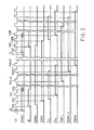
- Fig. 1 shows a preferred embodiment of a digital timing unit.
- the timing unit includes: a quartz oscillator 1, a flip-flop 2, three NOT elements respectively ( 3, 4,5) three AND gates 6, 7, 8 respective ly with three inputs (AND gates 6) and two inputs (AND gate 7 and 8), a four inputs NOR gate 9, a shift register 10, a set of n EXCLUSIVE OR gates G1, G2, ..., Gn and an auxiliary register 11.
- Shift register 10 has a data input INDAT and a set of output terminals TAPO, TAPN.
- Auxiliary register 11 has a set of inputs 11, ... In and a corresponding set of outputs 01, ..., On.
- the above mentioned elements are interconnected as follows.
- the output of oscillator 1 is connected to the clock input of flip-flop 2 and of register 10, 11.
- the direct output Q of flip-flop 2 is connected to a first input of AND gate 7 and to the input of NOT 4 whose output is connected to a first input of AND gate 6.
- the output terminal TAPN of register 10 is connected to a first input of AND gate 8, to a second input of AND gate 7, as well as to the input of NOT 5 whose output is connected to a second input of AND gate 6.
- the output On of register 11 is connected to a second input of AND ga te 8 and to the input of NOT 3, whose output is connected to the third input of AND gate 6.
- NOR gate 9 receives, through lead 12, an external RESET signal for ini tialization purpose.
- NOR gate 9 The output of NOR gate 9 is connected to the data input INDAT of shift register 10.
- Output terminals TAP 0, .... TAPN, of shift register 10; are suitably connected in pairs to the inputs of the n EXCLUSIVE OR gates Gl ... Gn depending on the timing requirements.
- Flip-flop 2 of JK type receives at input J, through lead 14, a START signal.
- the operation of the timing unit is the following:
- Register 10 is forced in a known initial reset status where each of its cells is at logical/electrical level 0, by means of a RESET pulse applied on lead 12 and having a length at least equal to T(N+1) where T is the oscillator period and (N+1) the cell number of shift register 10.
- the logical level 0 present at terminal TAPN inhibits AND gates 7 and 8.
- START pulse must have a minimum length greater than three ) clock periods.
- a logical level 1 propagates in shift register 10 and produces, owing to the connections between terminals TAPi and inputs of gates Gi, the generation of timing signals of a predetermined length which develops in a timing cycle.
- Such signals are transferred, for use by external circuits, through re gister 11.
- Register 11 function is only to synchronize the start and the end of timing signals with clock pulses, avoiding the spread which may be cau sed by gates Gi owing to the different propagation times such gates may have.
- register 11 may be constituted by single integrated circuit or by few of them.
- a logical level 0 is produced at the output of NOR gate 9, independen tly from the logical level present at output Q.
- shift register 10 during the subsequent clock is maintained in a discharged status untill a new START signal is received.
- timing unit object of the invention may perform identical timing cycles starting from two possible initial status and terminating in one of two possible status.
- a start command received by the unit enable the unit itself to pass from an initial status to the other one.
- a signal in output from gate Gn may be considered a feedback signal which maintain the unit enabled, even though the start command is removed, for the time necessary to complete the timing cycle.
- the signal in output from terminal TAPN may be considered a feedback signal which maintain the timing unit in one of the two possible ini- - tial status reached at the end of a cycle.
- circuit formed by gates 6, 7, 8, 9 and by NOT 3, 4, 5 and by flip-flop 2 can be embodied by different components, provided the same operation is performed, that is:
- register 11 too is not essential for the invention purposes even though it is suggested to cut at the minimum the spread of the starting and ending istants of the timing signal as to the clock pulses.
- EXCLUSIVE OR input Gn is to be connected to a terminal TAPN.
- connection of an input of gate Gn to terminal TAP 0 may be repla ced by the connection to an intermediate terminal TAPi.
- timing unit may be modified for generation of timing cycles of different length according to conditions or events which may occur during a cycle.
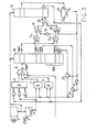
- Fig. 3 shows a variant to timing unit of fig. 1 for the purpose of ge nerating timing cycles of different length.
- Timing unit 3 includes all the circuital elements of fig. 1 identified by the same differences numbers.
- Shift register 10 comprises a "tail" 10A with M cells, each one havirg an output terminal TAPN +1, ..., TAPM.
- EXCLUSIVE OR of which only the EXCLUSIVE OR Gm is shown, two NOT circuits 16, 17, two AND gates 18, 19 an OR gate 20, two transferring gates of "tristate" type 21, 22 and an RS type flipf-flop 23.
- Inputs of EXCLUSIVE OR Gm are respectively connected to terminals TAPO and TAP M-1.
- EXCLUSIVE OR Gn and Gm are respectively connected to a first input of AND gates 18, 19 whose outputs are connected to the in puts of OR 20.
- OR 20 The output of OR 20 is connected to input In of register 11.
- Flip-flop 23 receives at its set input a signal of verified condition CV and at its reset input a timing signal coming from a cell of register 10.
- Such timing signal is generated at the beginning of each timing cycle and causes or confirms the reset status of flip-flop 23.
- Direct output Q1 of flip-flop 23 is connected to a second input of AND gate 19 and to the enabling input of tristate 22.
- the input of tristate 21, 22 is respectively connected to terminals TAPN and TAPM and the outputs are connected together, to the input of NOT 5 and to an input of AND gates 7, 8.
- timing unit performs in the same way as the one of fig. 1.
- flip-flop 23 is set AND gate 19 and tristate 22 are enabled.
- EXCLUSIVE OR Gn the action performed by EXCLUSIVE OR Gn is carried out by the EXCLUSIVE OR Gm and the signal in output from terminal TAPM substitutes for the signal in output from terminal TAPN.
- the length of a timing cycle is therefore extended for M clock periods.
- timing cycle extension additional timing ' signals may be generated and some timing signals, already started during the normal cycle, may be extended.
- timing unit when a timing unit is designed to supply a certain . number n of timing signals at outputs 0 1 ... 0 n , the length and the relative timing of such signals may be varied as follows.
- This may be carried out by the modification of the printing circuit supporting the components or by effecting such connections through straps changeable according to the needs.
- a list of preferred components available on the market for implemen tation of the timing unit object of the invention is supplied.
- TRISTATE 21,22 Integrated circuit 74 F 241 manufactured by FAIRCHILD
- the component include 8 tristates.
- EXCLUSIVE OR G Integrated circuit 74 F 86 manufactured by FAIRCHILD Propagation time 5 nsec.
- the component includes 4 EXCLUSIVE OR. Considering the propagation time of the above components it appears that such circuits allow to implement a timing unit having a typical clock period of about 16 nsec. in case of Fig. 1 and of about 2 3 nsec. in case of Fig. 3.
Landscapes
- Physics & Mathematics (AREA)
- Nonlinear Science (AREA)
- Engineering & Computer Science (AREA)
- Theoretical Computer Science (AREA)
- General Engineering & Computer Science (AREA)
- General Physics & Mathematics (AREA)
- Manipulation Of Pulses (AREA)
- Pulse Circuits (AREA)
Applications Claiming Priority (2)
| Application Number | Priority Date | Filing Date | Title |
|---|---|---|---|
| IT20304/82A IT1151513B (it) | 1982-03-22 | 1982-03-22 | Unita' di temporizzazione digitale |
| IT2030482 | 1982-03-22 |
Publications (2)
| Publication Number | Publication Date |
|---|---|
| EP0089596A1 true EP0089596A1 (de) | 1983-09-28 |
| EP0089596B1 EP0089596B1 (de) | 1986-06-25 |
Family
ID=11165576
Family Applications (1)
| Application Number | Title | Priority Date | Filing Date |
|---|---|---|---|
| EP83102516A Expired EP0089596B1 (de) | 1982-03-22 | 1983-03-15 | Digitale Zeitsteuerungseinheit |
Country Status (5)
| Country | Link |
|---|---|
| US (1) | US4517681A (de) |
| EP (1) | EP0089596B1 (de) |
| JP (1) | JPS58205230A (de) |
| DE (1) | DE3364247D1 (de) |
| IT (1) | IT1151513B (de) |
Cited By (1)
| Publication number | Priority date | Publication date | Assignee | Title |
|---|---|---|---|---|
| WO2000019608A3 (de) * | 1998-09-30 | 2000-11-23 | Koninkl Philips Electronics Nv | Schaltungsanordnung zum verarbeiten von datensignalen |
Families Citing this family (6)
| Publication number | Priority date | Publication date | Assignee | Title |
|---|---|---|---|---|
| JPS6286949A (ja) * | 1985-10-11 | 1987-04-21 | Mitsubishi Electric Corp | デ−タ受信方式 |
| DE3914006C1 (de) * | 1989-04-27 | 1990-06-28 | Siemens Ag, 1000 Berlin Und 8000 Muenchen, De | |
| RU2136111C1 (ru) * | 1998-06-11 | 1999-08-27 | Войсковая часть 25714 | Устройство для цикловой синхронизации |
| RU2224378C1 (ru) * | 2002-05-30 | 2004-02-20 | В/ч 25714 | Устройство для цикловой синхронизации |
| RU2237374C1 (ru) * | 2003-02-10 | 2004-09-27 | Войсковая часть 45807 | Устройство для цикловой синхронизации |
| RU2256295C1 (ru) * | 2004-01-19 | 2005-07-10 | Войсковая часть 45807 | Устройство для цикловой синхронизации |
Citations (4)
| Publication number | Priority date | Publication date | Assignee | Title |
|---|---|---|---|---|
| US3108227A (en) * | 1960-05-02 | 1963-10-22 | Philco Corp | Pattern suppressed ring counters |
| GB1018075A (en) * | 1961-07-28 | 1966-01-26 | Gen Electric | Circuit arrangement for generating a multiphase signal |
| US3564429A (en) * | 1969-02-05 | 1971-02-16 | Us Navy | Programmable rate oscillator |
| US4134073A (en) * | 1976-07-12 | 1979-01-09 | Honeywell Information Systems Inc. | Clock system having adaptive synchronization feature |
Family Cites Families (3)
| Publication number | Priority date | Publication date | Assignee | Title |
|---|---|---|---|---|
| US3648237A (en) * | 1969-02-28 | 1972-03-07 | Ibm | Apparatus and method for obtaining synchronization of a maximum length pseudorandom sequence |
| JPS5518085B2 (de) * | 1974-08-14 | 1980-05-16 | ||
| US4093997A (en) * | 1976-09-17 | 1978-06-06 | General Electric Company | Portable programmer for time-of-day metering register system and method of using same |
-
1982
- 1982-03-22 IT IT20304/82A patent/IT1151513B/it active
-
1983
- 1983-03-14 US US06/474,915 patent/US4517681A/en not_active Expired - Fee Related
- 1983-03-15 DE DE8383102516T patent/DE3364247D1/de not_active Expired
- 1983-03-15 EP EP83102516A patent/EP0089596B1/de not_active Expired
- 1983-03-22 JP JP58047792A patent/JPS58205230A/ja active Pending
Patent Citations (4)
| Publication number | Priority date | Publication date | Assignee | Title |
|---|---|---|---|---|
| US3108227A (en) * | 1960-05-02 | 1963-10-22 | Philco Corp | Pattern suppressed ring counters |
| GB1018075A (en) * | 1961-07-28 | 1966-01-26 | Gen Electric | Circuit arrangement for generating a multiphase signal |
| US3564429A (en) * | 1969-02-05 | 1971-02-16 | Us Navy | Programmable rate oscillator |
| US4134073A (en) * | 1976-07-12 | 1979-01-09 | Honeywell Information Systems Inc. | Clock system having adaptive synchronization feature |
Non-Patent Citations (2)
| Title |
|---|
| COMPUTER DESIGN, vol. 18, no. 12, December 1979, pages 104-107, Littleton, USA * |
| IBM TECHNICAL DISCLOSURE BULLETIN, vol. 24, no. 7A, December 1981, pages 3514-3515, New York, USA * |
Cited By (2)
| Publication number | Priority date | Publication date | Assignee | Title |
|---|---|---|---|---|
| WO2000019608A3 (de) * | 1998-09-30 | 2000-11-23 | Koninkl Philips Electronics Nv | Schaltungsanordnung zum verarbeiten von datensignalen |
| US6498817B1 (en) | 1998-09-30 | 2002-12-24 | Koninklijke Philips Electronics N.V. | Circuit for processing data signals |
Also Published As
| Publication number | Publication date |
|---|---|
| EP0089596B1 (de) | 1986-06-25 |
| IT1151513B (it) | 1986-12-24 |
| DE3364247D1 (en) | 1986-07-31 |
| JPS58205230A (ja) | 1983-11-30 |
| IT8220304A0 (it) | 1982-03-22 |
| IT8220304A1 (it) | 1983-09-22 |
| US4517681A (en) | 1985-05-14 |
Similar Documents
| Publication | Publication Date | Title |
|---|---|---|
| EP0711472B1 (de) | Verfahren und Vorrichtung zur Phasenverschiebung eines Taktsignals | |
| US6924684B1 (en) | Counter-based phase shifter circuits and methods with optional duty cycle correction | |
| US6252526B1 (en) | Circuit and method for fast parallel data strobe encoding | |
| US6629250B2 (en) | Adjustable data delay using programmable clock shift | |
| EP0704975A1 (de) | Digitaler phasenverriegelter Kreis mit grob- und feinstufig variabel einstellbaren Verzögerungsleitungen | |
| US5555213A (en) | Interface circuit, system and method for interfacing an electronic device and a synchronous state machine having different clock speeds | |
| EP0254406A2 (de) | Schaltkreis für Taktsignale | |
| CN101378258A (zh) | 一种模块化分频单元及分频器 | |
| JP2002208844A (ja) | グリッチ除去回路 | |
| EP0089596A1 (de) | Digitale Zeitsteuerungseinheit | |
| JPH0758609A (ja) | グリッチ抑制回路及び方法 | |
| WO2008008297A2 (en) | Glitch-free clock switcher | |
| KR20000070091A (ko) | 듀얼 에지 트리거 플립 플롭을 갖는 전자 회로 | |
| US4399377A (en) | Selectively operable bit-serial logic circuit | |
| US4234849A (en) | Programmable frequency divider and method | |
| US5185537A (en) | Gate efficient digital glitch filter for multiple input applications | |
| US5187385A (en) | Latch circuit including filter for metastable prevention | |
| US6791384B2 (en) | Delay adjustment circuit for delay locked loop | |
| US4654599A (en) | Four phase clock signal generator | |
| US6882184B2 (en) | Clock switching circuit | |
| US6091794A (en) | Fast synchronous counter | |
| US4387341A (en) | Multi-purpose retimer driver | |
| US5642060A (en) | Clock generator | |
| JP2002517935A (ja) | 異なる周波数のクロック信号を生成するための同調可能なディジタル発振器回路及び方法 | |
| JPH02168308A (ja) | クロック信号供給装置 |
Legal Events
| Date | Code | Title | Description |
|---|---|---|---|
| PUAI | Public reference made under article 153(3) epc to a published international application that has entered the european phase |
Free format text: ORIGINAL CODE: 0009012 |
|
| AK | Designated contracting states |
Designated state(s): DE FR GB |
|
| 17P | Request for examination filed |
Effective date: 19831213 |
|
| GRAA | (expected) grant |
Free format text: ORIGINAL CODE: 0009210 |
|
| AK | Designated contracting states |
Kind code of ref document: B1 Designated state(s): DE FR GB |
|
| REF | Corresponds to: |
Ref document number: 3364247 Country of ref document: DE Date of ref document: 19860731 |
|
| ET | Fr: translation filed | ||
| PLBE | No opposition filed within time limit |
Free format text: ORIGINAL CODE: 0009261 |
|
| STAA | Information on the status of an ep patent application or granted ep patent |
Free format text: STATUS: NO OPPOSITION FILED WITHIN TIME LIMIT |
|
| 26N | No opposition filed | ||
| PGFP | Annual fee paid to national office [announced via postgrant information from national office to epo] |
Ref country code: DE Payment date: 19920120 Year of fee payment: 10 |
|
| PGFP | Annual fee paid to national office [announced via postgrant information from national office to epo] |
Ref country code: GB Payment date: 19920303 Year of fee payment: 10 |
|
| PGFP | Annual fee paid to national office [announced via postgrant information from national office to epo] |
Ref country code: FR Payment date: 19920326 Year of fee payment: 10 |
|
| PG25 | Lapsed in a contracting state [announced via postgrant information from national office to epo] |
Ref country code: GB Effective date: 19930315 |
|
| GBPC | Gb: european patent ceased through non-payment of renewal fee |
Effective date: 19930315 |
|
| PG25 | Lapsed in a contracting state [announced via postgrant information from national office to epo] |
Ref country code: FR Effective date: 19931130 |
|
| PG25 | Lapsed in a contracting state [announced via postgrant information from national office to epo] |
Ref country code: DE Effective date: 19931201 |
|
| REG | Reference to a national code |
Ref country code: FR Ref legal event code: ST |