EP0084393B1 - Dispositif semiconducteur du genre transistor à hétérojonction(s) - Google Patents
Dispositif semiconducteur du genre transistor à hétérojonction(s) Download PDFInfo
- Publication number
- EP0084393B1 EP0084393B1 EP83200040A EP83200040A EP0084393B1 EP 0084393 B1 EP0084393 B1 EP 0084393B1 EP 83200040 A EP83200040 A EP 83200040A EP 83200040 A EP83200040 A EP 83200040A EP 0084393 B1 EP0084393 B1 EP 0084393B1
- Authority
- EP
- European Patent Office
- Prior art keywords
- layer
- region
- semiconductor
- semiconductor device
- undoped
- Prior art date
- Legal status (The legal status is an assumption and is not a legal conclusion. Google has not performed a legal analysis and makes no representation as to the accuracy of the status listed.)
- Expired
Links
- 239000004065 semiconductor Substances 0.000 title claims description 61
- 239000000463 material Substances 0.000 claims description 36
- JBRZTFJDHDCESZ-UHFFFAOYSA-N AsGa Chemical compound [As]#[Ga] JBRZTFJDHDCESZ-UHFFFAOYSA-N 0.000 claims description 25
- 229910001218 Gallium arsenide Inorganic materials 0.000 claims description 24
- 229910052782 aluminium Inorganic materials 0.000 claims description 17
- XAGFODPZIPBFFR-UHFFFAOYSA-N aluminium Chemical compound [Al] XAGFODPZIPBFFR-UHFFFAOYSA-N 0.000 claims description 17
- 230000000694 effects Effects 0.000 claims description 10
- GYHNNYVSQQEPJS-UHFFFAOYSA-N Gallium Chemical compound [Ga] GYHNNYVSQQEPJS-UHFFFAOYSA-N 0.000 claims description 7
- 229910052733 gallium Inorganic materials 0.000 claims description 7
- 239000004411 aluminium Substances 0.000 claims description 6
- MDPILPRLPQYEEN-UHFFFAOYSA-N aluminium arsenide Chemical compound [As]#[Al] MDPILPRLPQYEEN-UHFFFAOYSA-N 0.000 claims description 6
- 238000009825 accumulation Methods 0.000 claims description 5
- 230000005684 electric field Effects 0.000 claims description 5
- 230000010287 polarization Effects 0.000 claims description 5
- 239000002800 charge carrier Substances 0.000 claims description 4
- 230000007423 decrease Effects 0.000 claims description 4
- 229910052732 germanium Inorganic materials 0.000 claims description 4
- GNPVGFCGXDBREM-UHFFFAOYSA-N germanium atom Chemical compound [Ge] GNPVGFCGXDBREM-UHFFFAOYSA-N 0.000 claims description 4
- 229910052737 gold Inorganic materials 0.000 claims description 4
- 239000010931 gold Substances 0.000 claims description 4
- 238000012546 transfer Methods 0.000 claims description 4
- 229910052785 arsenic Inorganic materials 0.000 claims description 3
- PCHJSUWPFVWCPO-UHFFFAOYSA-N gold Chemical compound [Au] PCHJSUWPFVWCPO-UHFFFAOYSA-N 0.000 claims description 3
- 239000000758 substrate Substances 0.000 claims description 3
- RQNWIZPPADIBDY-UHFFFAOYSA-N arsenic atom Chemical compound [As] RQNWIZPPADIBDY-UHFFFAOYSA-N 0.000 claims description 2
- 150000002343 gold Chemical class 0.000 claims 1
- 238000010586 diagram Methods 0.000 description 13
- 239000012535 impurity Substances 0.000 description 9
- 239000000969 carrier Substances 0.000 description 4
- 150000001875 compounds Chemical class 0.000 description 4
- 239000003574 free electron Substances 0.000 description 4
- 230000003993 interaction Effects 0.000 description 4
- 230000004888 barrier function Effects 0.000 description 3
- 239000011651 chromium Substances 0.000 description 3
- 238000000034 method Methods 0.000 description 3
- 230000007704 transition Effects 0.000 description 3
- 230000005533 two-dimensional electron gas Effects 0.000 description 3
- VYZAMTAEIAYCRO-UHFFFAOYSA-N Chromium Chemical compound [Cr] VYZAMTAEIAYCRO-UHFFFAOYSA-N 0.000 description 2
- XUIMIQQOPSSXEZ-UHFFFAOYSA-N Silicon Chemical compound [Si] XUIMIQQOPSSXEZ-UHFFFAOYSA-N 0.000 description 2
- 230000008859 change Effects 0.000 description 2
- 229910052804 chromium Inorganic materials 0.000 description 2
- 239000011669 selenium Substances 0.000 description 2
- 229910052710 silicon Inorganic materials 0.000 description 2
- 239000010703 silicon Substances 0.000 description 2
- 241001415961 Gaviidae Species 0.000 description 1
- 229910000927 Ge alloy Inorganic materials 0.000 description 1
- BUGBHKTXTAQXES-UHFFFAOYSA-N Selenium Chemical compound [Se] BUGBHKTXTAQXES-UHFFFAOYSA-N 0.000 description 1
- 241001080024 Telles Species 0.000 description 1
- BYDQGSVXQDOSJJ-UHFFFAOYSA-N [Ge].[Au] Chemical compound [Ge].[Au] BYDQGSVXQDOSJJ-UHFFFAOYSA-N 0.000 description 1
- 230000008901 benefit Effects 0.000 description 1
- 230000015572 biosynthetic process Effects 0.000 description 1
- 230000015556 catabolic process Effects 0.000 description 1
- 239000013078 crystal Substances 0.000 description 1
- 230000003247 decreasing effect Effects 0.000 description 1
- 238000000151 deposition Methods 0.000 description 1
- 238000011161 development Methods 0.000 description 1
- 238000009792 diffusion process Methods 0.000 description 1
- 238000009826 distribution Methods 0.000 description 1
- 238000000407 epitaxy Methods 0.000 description 1
- 238000002474 experimental method Methods 0.000 description 1
- 230000005669 field effect Effects 0.000 description 1
- 238000004519 manufacturing process Methods 0.000 description 1
- 238000001451 molecular beam epitaxy Methods 0.000 description 1
- 230000005693 optoelectronics Effects 0.000 description 1
- 125000002524 organometallic group Chemical group 0.000 description 1
- 230000008569 process Effects 0.000 description 1
- 230000006798 recombination Effects 0.000 description 1
- 238000005215 recombination Methods 0.000 description 1
- 229910052711 selenium Inorganic materials 0.000 description 1
- 238000000926 separation method Methods 0.000 description 1
- 238000004088 simulation Methods 0.000 description 1
- 239000007787 solid Substances 0.000 description 1
- WFKWXMTUELFFGS-UHFFFAOYSA-N tungsten Chemical compound [W] WFKWXMTUELFFGS-UHFFFAOYSA-N 0.000 description 1
- 229910052721 tungsten Inorganic materials 0.000 description 1
- 239000010937 tungsten Substances 0.000 description 1
- 238000000927 vapour-phase epitaxy Methods 0.000 description 1
Images

Classifications
-
- H—ELECTRICITY
- H10—SEMICONDUCTOR DEVICES; ELECTRIC SOLID-STATE DEVICES NOT OTHERWISE PROVIDED FOR
- H10D—INORGANIC ELECTRIC SEMICONDUCTOR DEVICES
- H10D62/00—Semiconductor bodies, or regions thereof, of devices having potential barriers
- H10D62/80—Semiconductor bodies, or regions thereof, of devices having potential barriers characterised by the materials
- H10D62/82—Heterojunctions
- H10D62/824—Heterojunctions comprising only Group III-V materials heterojunctions, e.g. GaN/AlGaN heterojunctions
-
- H—ELECTRICITY
- H10—SEMICONDUCTOR DEVICES; ELECTRIC SOLID-STATE DEVICES NOT OTHERWISE PROVIDED FOR
- H10D—INORGANIC ELECTRIC SEMICONDUCTOR DEVICES
- H10D48/00—Individual devices not covered by groups H10D1/00 - H10D44/00
- H10D48/30—Devices controlled by electric currents or voltages
- H10D48/32—Devices controlled by only the electric current supplied, or only the electric potential applied, to an electrode which does not carry the current to be rectified, amplified or switched
- H10D48/36—Unipolar devices
- H10D48/362—Unipolar transistors having ohmic electrodes on emitter-like, base-like, and collector-like regions, e.g. hot electron transistors [HET], metal base transistors [MBT], resonant tunnelling transistors [RTT], bulk barrier transistors [BBT], planar doped barrier transistors [PDBT] or charge injection transistors [CHINT]
Definitions
- the invention relates to a semiconductor device, of the heterojunction transistor type, comprising a stack of semiconductor layers which, by combination, form three regions called source, gate and drain, while the current path which s established between said source and drain regions is substantially perpendicular to the various junctions.
- the invention relates to semiconductor devices, more specifically to heterojunction transistors.
- Heterojunction (s) structures are well known in the prior art as having been designed and tested in the 1950s and following. But, although having very interesting potential characteristics, superior to those of homojunctions, they have been very little developed except perhaps in opto-electronic devices, such as lasers. Thus, although numerous works and publications have been made public on heterojunction (s) semiconductor devices, the main applications developed on the market are of the homojunction (s) type.
- EP-A-0 027 761 entitled: “Semiconductor device with field effect, for high frequencies, and transistor and device with charge transfer using such a semiconductor device •, which describes a horizontal type transistor, the gate region of which has a P / N anisotype junction (GaAs P / Ga 1-x Al x AsN), in which a layer d 'charge inversion for a positive polarization of the gate region.
- the semiconductor device according to the present invention consists of a stack of semiconductor layers forming by combination the three source, gate and drain regions, and the current path which flows from the source to the drain is substantially perpendicular to the various junctions.
- heterojunction semiconductor devices are known from the prior art and mention will be made, for example, of patent US Pat. No. 4,119,994 which describes heterojunction transistors of conventional type, that is to say of which an area of a first type of conductivity (called base area) is placed between two areas of the second type of conductivity (called emitter and collector areas).
- base area an area of a first type of conductivity
- emitter and collector areas two areas of the second type of conductivity
- the semiconductor device does not belong to this type of transistor; it is a new structure which belongs to the family of the transistors, in which all the transport of charges are carried out by electrons being majority carriers.
- the device uses both ballistic or quasi-ballistic transport for the current going from the source to the drain and conduction in a two-dimensional Fermi quasi-gas for conduction in the grid.
- the carriers of the current going from the source to the drain cross this Fermi gas perpendicularly or almost perpendicularly without having much interaction with the carriers which constitute said gas.
- the two-dimensional electron gas in the vicinity of a heterojunction is for example described in the article by H.L. STORMER et al. entitled: "Two dimensional electron gas at a semiconductor- semiconductor interface which appeared in Solid State Communications, Vol. 29, p. 705-709, 1979.
- the semiconductor device is remarkable in that the second region called the gate consists of a layer of a first semiconductor material, which forms a first heterojunction with the layer immediately adjacent to the third region called the drain, in a second semiconductor material, while said first and second semiconductor materials are chosen such that, at heterojunction, the lower level of the conduction band in the first semiconductor material is located below the lower level of the conduction band in the second semiconductor material, and while, under the effect of the component of the electric field, normal to the heterojunction, there is formed in the second region called the grid, in the vicinity of the heterojunction, an accumulation zone d electrons constituting a two-dimensional Fermi quasi-gas in a potential well, the lower level of which is controlled by a grill electrode the, and in that the first region, called the source region, comprises at least one layer, of which at least that in contact with the source electrode is very heavily n-type doped in a third semiconductor material, chosen so that the lower level of the conduction band in the third semiconductor material can, by means of the bias
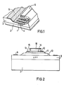
- the semiconductor device is taken from the article “Fabrication and Numerical Simulation of the Permeable Base Transistor”, by CO BOZLER and GD ALLEY, in IEEE Transactions on Electron Devices, Flight. ED-27, No. 6, June 1980.
- An emitter contact, referenced 1, of the ohmic type is taken from a heavily doped region, of the n + type, of gallium arsenide 2; the flow of electrons emitted by this contact 1 is confined by insulating regions 3, obtained for example by a bombardment of protons, in a region 4 normally doped of type n, and thus crosses a grid 5 formed of a multitude of fingers embedded in the semiconductor material to finally reach the collector contact 6, also of the ohmic type.
- the grid 5 is formed for example by tungsten which makes a Schottky type contact with the gallium arsenide; its role is to control the flow of electrons which pass from the emitter to the collector, in a manner somewhat analogous to a triode in a vacuum, despite the important role played by the diffusion currents in this device.
- the maximum transition frequency (the current gain is equal to unity) is generally defined by the formula: in which g m represents the transconductance and C T is calculated from the total variation of charge in the semiconductor ⁇ QT, produced by a variation of the potential of the grid electrode ⁇ V GS
- the devices produced according to these teachings have a maximum frequency f T , as defined above, of the order of 40 GHz.
- the cut-off frequency or maximum operating frequency is around 10 GHz.
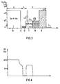
- a device according to the present invention is shown in a sectional view in FIG. 2.
- a semi-insulating substrate 7 such as for example gallium arsenide, doped with chromium
- a semiconductor layer 8 is grown by epitaxy. heavily doped, of conductivity type n ++ , with doping of the order of 10 18 atoms. cm-3 obtained for example by introduction of silicon impurities and a non-critical thickness, for example 0.5 micron.
- This layer 8 serves as a drain electrode, and an ohmic contact 9, for example from a gold-germanium alloy can be taken around the periphery of the device, for example in the form of a crown.
- a layer 10 lightly doped of type n conductivity is produced with a doping for example of the order of 10 16 atoms - cm-3, or even undoped, in a semiconductor material such as gallium arsenide, with a thickness close to 0.5 micron.
- the essential function of this layer 10 is to separate the layer 8 from the upper layers and therefore to decrease the capacity between the drain electrode formed by the heavily doped layer 8 and the two-dimensional Fermi gas which functions as a gate electrode in layer 12 while also increasing the drain-gate breakdown voltage.
- this layer 11 is composed of Ga 1 _ X Al X As, lightly doped n, with a constant and sufficient aluminum fractional value.
- this layer 11 is in fact formed of three zones, with, in the vicinity of the junction with the upper layer 12, a first undoped zone with a thickness close to 5 nm and a fractional value x out of aluminum which varies continuously from approximately 0.2 to 0.3, then a second very heavily doped zone, of conductivity type n ++ , with a doping level of 1 0 18 atoms.
- cm- 3 cm- 3 , a thickness close to 10 nm and a fractional value x in aluminum which is constant at around 0.3, and finally a third undoped zone, with a thickness close to 85 nm and a fractional value in aluminum which is constant at 0.3 approximately, then decreasing at the end of the zone until it becomes zero, for example linearly.
- this layer 11 is undoped, in gallium and aluminum arsenide Ga 1 _ X Al X As and a fractional value x in aluminum varying by level, as in the previous embodiment.
- Layer 12 is a layer made of another semiconductor compound chosen so that its lower level of the conduction band is located below the lower level of the conduction band of layer 11, and only under the effect of the component electric field, normal to the heterojunction between the two above-mentioned layers 11/12, a potential well is formed there; the curvature of the conduction band must be sufficient for the lower level to cross the Fermi level in the vicinity of the heterojunction, thus authorizing an accumulation of electrons in this vicinity, as shown in FIG. 5 which will be more fully discussed below. -after.
- the layer 11 is made of gallium and aluminum Ga 1 - x Al x As arsenide
- the layer 12 is made of gallium arsenide GaAs, undoped.
- An example of possible choice for the materials constituting the layers 11 and 12 is the GaAIAs / GaAs pair, but other materials are possible.
- the Applicant has preferentially chosen the GaAIAs / GaAs pair which has the advantage of an equivalent structure and of a crystalline mesh, which associates without significant disturbance of the order crystalline.
- This electronic enrichment zone occupies a very small thickness, less than 5 nm, in a GaAs layer of thickness close to 50 nm, which constitutes what should be called the gate region of this new structure.
- the gate contact capable of controlling the Fermi level (or quasi-level) of the aforesaid gate region, is obtained by a layer 13, in ohmic contact with said layer 12 in GaAs, deposited for example in the form of a crown around the periphery of this intermediate plate, for example by stacking a layer of gold on a layer of germanium.
- the source region of the new device is formed by all of the layers 14 and 15, on which a source electrode 16 is deposited.
- Layer 14 is an intermediate layer between layer 15 which serves as an electron source and the lower layers of the gate region.
- the essential function of this layer 14 is to provide the electrons leaving this layer 14 and entering the lower layer 12 of the gate region with an average kinetic energy, in the normal direction at the interface of the two above-mentioned layers 14 / 12, close to the difference in electronic affinity, between the materials forming these layers, called third and first semiconductor materials, for the layers of the source and gate regions respectively.
- the layer 14 consists of gallium arsenide and aluminum, undoped, of small thickness, for example 25 nm.
- Layer 15 which constitutes the electron source, also consists of gallium and aluminum arsenide, but very heavily doped, of type n and of doping greater than 10 18 atoms. cm-G, and of a non-critical thickness, for example of 200 nm.
- the source electrode is obtained in the form of an ohmic contact 16. According to an exemplary embodiment, this can be produced in the form of a layer of gallium arsenide, of conductivity type n, doped between 10 17 and 10 18 atoms - cm-3, on which a thin layer of germanium of type n conductivity, doped for example with arsenic, is deposited at 10 20 atoms - cm-3, and on which is finally taken metallic contact, for example by depositing gold or aluminum.
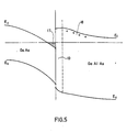
- FIG. 3 represents the variations in doping in the number of atoms per cubic centimeter.
- Doping of the negative conductivity type of the semiconductor compounds GaAs and Ga 1 - x Al x As is carried out for example by atoms of impurities such as silicon (Si) or selenium (Se).
- the substrate is semi-insulating and obtained for example by doping with chromium (Cr) of gallium arsenide (GaAs).
- the various source, grid and drain zones are also represented in this figure by the symbols S, G and D.
- dotted curves represent the various variants mentioned above.
- FIG. 4 represents the variations of the fractional value x in aluminum, of the compound Ga 1 - x Al x As, in the case of the example of embodiment described with the GaAs / GaAIAs couple. From a source region, in plateau, with a value of for example 0.45, we note an inflection at around 0.30 (layer 14) until reaching a value of around 0.20, inflection corresponding to a change in the slope of the curve which represents the above variations. Symmetrically, a second plateau region, with a value of for example 0.30 (layer 11) is reached, after an equivalent and symmetrical inflection to around 0.20.
- the inflection with change in slope of the variation curves of the aluminum fractional value x of the compound Ga 1-x Al x As has the essential aim of softening the curvature of the band levels, at the interface, so as to decrease the phenomenon of quantum reflection which occurs during the passage of an electron near a discontinuity of potential.
- FIG. 5 represents the band diagram, on either side of the main heterojunction.
- the left part of the diagram represents the GaAs material, and the right part the Ga 0.7 Al0 .3 As material (for example).
- the symbols E c and E v represent the lower and upper levels of the conduction or value band respectively.
- the symbol E f represents the Fermi level, that is to say the energy level for which the probability of occupation is equal to 0.5.
- the band curvatures are such that a zone 17 of electron accumulation appears.
- a thin layer 19, undoped, in the material Ga 1 - x Al x As is intended to ensure good separation between the donor impurities (for example Si) and this layer of localized electrons.
- This layer of localized electrons 17 forms a sort of quasi-Fermi gas, in two dimensions, while the polarization means 13 make it possible to bring it to the desired potential, of the order of a few tenths of volts, for example 0, 2 volts, relative to the source, and thus control the lower level of the potential well.
- figure 6 represents the diagrams of band of the whole of the device with the same potential (figure 6-a) or polarized (figures 6-b and 6-c).
- V, V 2
- the diagram of bands (figure 6-a) lets appear a potential well, so that the source-drain current is null.
- V i V 2
- electrons from the source can cross this potential well.
- ballistic effect it is meant in the present specification, that the charge carrier, in this case the electron, is accelerated without notable collision, neither with the impurities present in the crystal lattice, nor with the phonons (vibrations of the network) over a distance less than a critical length called free path.
- the mean free path before collision is greater, for example by the order of a micron.
- the figure 6-b represents the diagram of bands when the source potential (V 1 ) is lower than the drain potential (V 2 ) and that the gate potential (V 3 ) has an intermediate value:
- a part has electrons which are emitted by the source because of the potential difference between source and grid, passes the region of the grid with enough conservation of energy and impulse so that these electrons cross the discontinuity in the band of conduction between the gate and drain regions.
- the device according to the present invention has properties that are far more advantageous than all the current known devices, in particular in that the maximum transition frequency f T , which can be approximated by the following formula: is higher than 100 GHz.
Landscapes
- Junction Field-Effect Transistors (AREA)
- Bipolar Transistors (AREA)
Applications Claiming Priority (2)
| Application Number | Priority Date | Filing Date | Title |
|---|---|---|---|
| FR8200682 | 1982-01-18 | ||
| FR8200682A FR2520157B1 (fr) | 1982-01-18 | 1982-01-18 | Dispositif semi-conducteur du genre transistor a heterojonction(s) |
Publications (3)
| Publication Number | Publication Date |
|---|---|
| EP0084393A2 EP0084393A2 (fr) | 1983-07-27 |
| EP0084393A3 EP0084393A3 (en) | 1983-08-10 |
| EP0084393B1 true EP0084393B1 (fr) | 1986-04-16 |
Family
ID=9270068
Family Applications (1)
| Application Number | Title | Priority Date | Filing Date |
|---|---|---|---|
| EP83200040A Expired EP0084393B1 (fr) | 1982-01-18 | 1983-01-12 | Dispositif semiconducteur du genre transistor à hétérojonction(s) |
Country Status (6)
| Country | Link |
|---|---|
| US (1) | US4758868A (enExample) |
| EP (1) | EP0084393B1 (enExample) |
| JP (1) | JPS58127383A (enExample) |
| CA (1) | CA1210527A (enExample) |
| DE (1) | DE3362975D1 (enExample) |
| FR (1) | FR2520157B1 (enExample) |
Families Citing this family (25)
| Publication number | Priority date | Publication date | Assignee | Title |
|---|---|---|---|---|
| US4910562A (en) * | 1982-04-26 | 1990-03-20 | International Business Machines Corporation | Field induced base transistor |
| US4532533A (en) * | 1982-04-27 | 1985-07-30 | International Business Machines Corporation | Ballistic conduction semiconductor device |
| JPH0810763B2 (ja) * | 1983-12-28 | 1996-01-31 | 株式会社日立製作所 | 半導体装置 |
| US4712122A (en) * | 1984-07-26 | 1987-12-08 | Research Development Corp. | Heterojunction gate ballistic JFET with channel thinner than Debye length |
| US4800415A (en) * | 1984-09-21 | 1989-01-24 | American Telephone And Telegraph Company, At&T Bell Laboratories | Bipolar inversion channel device |
| US4691215A (en) * | 1985-01-09 | 1987-09-01 | American Telephone And Telegraph Company | Hot electron unipolar transistor with two-dimensional degenerate electron gas base with continuously graded composition compound emitter |
| JPH088350B2 (ja) * | 1985-04-08 | 1996-01-29 | 日本電気株式会社 | 半導体装置 |
| JPS61248561A (ja) * | 1985-04-25 | 1986-11-05 | インタ−ナショナル・ビジネス・マシ−ンズ・コ−ポレ−ション | 半導体構造体 |
| US4806997A (en) * | 1985-06-14 | 1989-02-21 | AT&T Laboratories American Telephone and Telegraph Company | Double heterostructure optoelectronic switch |
| US5059545A (en) * | 1985-08-23 | 1991-10-22 | Texas Instruments Incorporated | Three terminal tunneling device and method |
| US4959696A (en) * | 1985-08-23 | 1990-09-25 | Texas Instruments Incorporated | Three terminal tunneling device and method |
| EP0216155A3 (en) * | 1985-08-23 | 1989-03-15 | Texas Instruments Incorporated | Three-terminal tunnelling device |
| US4994882A (en) * | 1986-11-05 | 1991-02-19 | University Of Illinois | Semiconductor device and method |
| FR2611305B1 (fr) * | 1987-02-20 | 1990-04-27 | Labo Electronique Physique | Circuit comportant des lignes conductrices pour le transfert de signaux rapides |
| EP0314836A1 (en) * | 1987-11-06 | 1989-05-10 | Max-Planck-Gesellschaft zur Förderung der Wissenschaften e.V. | Semiconductor device in particular a hot electron transistor |
| US5172194A (en) * | 1987-09-16 | 1992-12-15 | National Science Council | Structures of modulation doped base hot electron transistors |
| US4872744A (en) * | 1988-01-15 | 1989-10-10 | Bell Communications Research, Inc. | Single quantum well optical modulator |
| US5023671A (en) * | 1989-03-27 | 1991-06-11 | International Business Machines Corporation | Microstructures which provide superlattice effects and one-dimensional carrier gas channels |
| US5179037A (en) * | 1991-12-24 | 1993-01-12 | Texas Instruments Incorporated | Integration of lateral and vertical quantum well transistors in the same epitaxial stack |
| US8080824B2 (en) * | 2006-11-15 | 2011-12-20 | Academia Sinica | Suppressing recombination in an electronic device |
| USD713655S1 (en) | 2013-05-31 | 2014-09-23 | Zzz Sock, LLC | Mattress cover |
| US9265368B2 (en) | 2013-05-31 | 2016-02-23 | Zzz Sock, LLC | Bedding apparatus |
| USD792124S1 (en) | 2013-05-31 | 2017-07-18 | Zzz Sock, LLC | Mattress cover |
| US9247835B2 (en) | 2013-05-31 | 2016-02-02 | Zzz Sock, LLC | Bedding apparatus |
| CA2972678C (en) * | 2015-01-12 | 2022-07-26 | Helmut WEIDLICH | Device for guiding charge carriers and use thereof |
Family Cites Families (13)
| Publication number | Priority date | Publication date | Assignee | Title |
|---|---|---|---|---|
| US4163237A (en) * | 1978-04-24 | 1979-07-31 | Bell Telephone Laboratories, Incorporated | High mobility multilayered heterojunction devices employing modulated doping |
| US4194935A (en) * | 1978-04-24 | 1980-03-25 | Bell Telephone Laboratories, Incorporated | Method of making high mobility multilayered heterojunction devices employing modulated doping |
| DE2847451C2 (de) * | 1978-11-02 | 1986-06-12 | Telefunken electronic GmbH, 7100 Heilbronn | Halbleiterbauelement und Verfahren zum Herstellen |
| FR2465318A1 (fr) * | 1979-09-10 | 1981-03-20 | Thomson Csf | Transistor a effet de champ a frequence de coupure elevee |
| FR2469002A1 (fr) * | 1979-10-26 | 1981-05-08 | Thomson Csf | Dispositif semiconducteur a effet de champ pour hautes frequences et transistor et dispositif a transfert de charges utilisant un tel semiconducteur |
| DE3072175D1 (de) * | 1979-12-28 | 1990-04-26 | Fujitsu Ltd | Halbleitervorrichtungen mit heterouebergang. |
| US4286275A (en) * | 1980-02-04 | 1981-08-25 | International Business Machines Corporation | Semiconductor device |
| JPS5946103B2 (ja) * | 1980-03-10 | 1984-11-10 | 日本電信電話株式会社 | トランジスタ |
| JPS56133867A (en) * | 1980-03-21 | 1981-10-20 | Semiconductor Res Found | Thermoelectric emission transistor |
| US4366493A (en) * | 1980-06-20 | 1982-12-28 | International Business Machines Corporation | Semiconductor ballistic transport device |
| FR2493604A1 (fr) * | 1980-10-31 | 1982-05-07 | Thomson Csf | Transistors a effet de champ a grille ultra courte |
| US4396931A (en) * | 1981-06-12 | 1983-08-02 | International Business Machines Corporation | Tunnel emitter upper valley transistor |
| US4460910A (en) * | 1981-11-23 | 1984-07-17 | International Business Machines Corporation | Heterojunction semiconductor |
-
1982
- 1982-01-18 FR FR8200682A patent/FR2520157B1/fr not_active Expired
-
1983
- 1983-01-12 DE DE8383200040T patent/DE3362975D1/de not_active Expired
- 1983-01-12 EP EP83200040A patent/EP0084393B1/fr not_active Expired
- 1983-01-13 CA CA000419430A patent/CA1210527A/en not_active Expired
- 1983-01-18 JP JP58006550A patent/JPS58127383A/ja active Granted
-
1987
- 1987-10-21 US US07/112,030 patent/US4758868A/en not_active Expired - Fee Related
Also Published As
| Publication number | Publication date |
|---|---|
| DE3362975D1 (en) | 1986-05-22 |
| US4758868A (en) | 1988-07-19 |
| CA1210527A (en) | 1986-08-26 |
| JPS58127383A (ja) | 1983-07-29 |
| FR2520157A1 (fr) | 1983-07-22 |
| EP0084393A2 (fr) | 1983-07-27 |
| FR2520157B1 (fr) | 1985-09-13 |
| JPH0261147B2 (enExample) | 1990-12-19 |
| EP0084393A3 (en) | 1983-08-10 |
Similar Documents
| Publication | Publication Date | Title |
|---|---|---|
| EP0084393A2 (fr) | Dispositif semiconducteur du genre transistor à hétérojonction(s) | |
| EP0017531B1 (fr) | Transistor à effet de champ à fréquence de coupure élevée et son procédé de réalisation | |
| EP0236189B1 (fr) | Structure semi-conductrice monolithique d'un transistor bipolaire à hétérojonction et d'un laser | |
| US5780916A (en) | Asymmetric contacted metal-semiconductor-metal photodetectors | |
| JPH054812B2 (enExample) | ||
| JP2622379B2 (ja) | オーム接点 | |
| JPS6313355B2 (enExample) | ||
| US5880482A (en) | Low dark current photodetector | |
| EP1243029B1 (fr) | Transistor bipolaire à hétérojonction collecteur en haut et procédé de réalisation | |
| JPH06291359A (ja) | 半導体受光素子 | |
| US20060267007A1 (en) | Devices incorporating heavily defected semiconductor layers | |
| FR2508707A1 (fr) | Transistor balistique a multiples heterojonctions | |
| JPH024140B2 (enExample) | ||
| EP0051504B1 (fr) | Transistors à effet de champ à grille ultra courte | |
| JPH07118531B2 (ja) | ホットエレクトロン・ユニポーラ・トランジスタ | |
| FR2568410A1 (fr) | Transistor statique a induction et son circuit integre | |
| EP0050064B1 (fr) | Transistor à effet de champ à fréquence de coupure élevée | |
| EP3353818A1 (fr) | Photodétecteur comprenant un empilement de couches superposées | |
| EP0522952B1 (fr) | Transistor à effet de champ, à couches minces de barrière et couche mince dopée | |
| US20070018192A1 (en) | Devices incorporating heavily defected semiconductor layers | |
| EP0232662B1 (fr) | Structure semi-conductrice monolithique d'un laser et d'un transistor à effet de champ et son procédé de fabrication | |
| FR2496990A1 (fr) | Transistor a effet de champ a barriere schottky | |
| CA1244149A (en) | Semiconductor ballistic electron velocity control structure | |
| US5162891A (en) | Group III-V heterostructure devices having self-aligned graded contact diffusion regions and method for fabricating same | |
| FR2569056A1 (fr) | Transistor a induction statique du type a injection par effet tunnel et circuit integre comprenant un tel transistor |
Legal Events
| Date | Code | Title | Description |
|---|---|---|---|
| PUAI | Public reference made under article 153(3) epc to a published international application that has entered the european phase |
Free format text: ORIGINAL CODE: 0009012 |
|
| PUAL | Search report despatched |
Free format text: ORIGINAL CODE: 0009013 |
|
| AK | Designated contracting states |
Designated state(s): DE FR GB IT NL |
|
| AK | Designated contracting states |
Designated state(s): DE FR GB IT NL |
|
| 17P | Request for examination filed |
Effective date: 19831005 |
|
| GRAA | (expected) grant |
Free format text: ORIGINAL CODE: 0009210 |
|
| AK | Designated contracting states |
Kind code of ref document: B1 Designated state(s): DE FR GB IT NL |
|
| REF | Corresponds to: |
Ref document number: 3362975 Country of ref document: DE Date of ref document: 19860522 |
|
| ITF | It: translation for a ep patent filed | ||
| PLBE | No opposition filed within time limit |
Free format text: ORIGINAL CODE: 0009261 |
|
| STAA | Information on the status of an ep patent application or granted ep patent |
Free format text: STATUS: NO OPPOSITION FILED WITHIN TIME LIMIT |
|
| 26N | No opposition filed | ||
| PGFP | Annual fee paid to national office [announced via postgrant information from national office to epo] |
Ref country code: NL Payment date: 19890131 Year of fee payment: 9 |
|
| REG | Reference to a national code |
Ref country code: FR Ref legal event code: CD |
|
| PG25 | Lapsed in a contracting state [announced via postgrant information from national office to epo] |
Ref country code: NL Effective date: 19910801 |
|
| NLV4 | Nl: lapsed or anulled due to non-payment of the annual fee | ||
| ITTA | It: last paid annual fee | ||
| ITPR | It: changes in ownership of a european patent |
Owner name: CAMBIO RAGIONE SOCIALE;PHILIPS ELECTRONICS N.V. |
|
| REG | Reference to a national code |
Ref country code: FR Ref legal event code: CJ Ref country code: FR Ref legal event code: CD |
|
| PGFP | Annual fee paid to national office [announced via postgrant information from national office to epo] |
Ref country code: GB Payment date: 19961224 Year of fee payment: 15 |
|
| PGFP | Annual fee paid to national office [announced via postgrant information from national office to epo] |
Ref country code: FR Payment date: 19970121 Year of fee payment: 15 |
|
| PGFP | Annual fee paid to national office [announced via postgrant information from national office to epo] |
Ref country code: DE Payment date: 19970319 Year of fee payment: 15 |
|
| PG25 | Lapsed in a contracting state [announced via postgrant information from national office to epo] |
Ref country code: GB Free format text: LAPSE BECAUSE OF NON-PAYMENT OF DUE FEES Effective date: 19980112 |
|
| PG25 | Lapsed in a contracting state [announced via postgrant information from national office to epo] |
Ref country code: FR Free format text: THE PATENT HAS BEEN ANNULLED BY A DECISION OF A NATIONAL AUTHORITY Effective date: 19980131 |
|
| GBPC | Gb: european patent ceased through non-payment of renewal fee |
Effective date: 19980112 |
|
| PG25 | Lapsed in a contracting state [announced via postgrant information from national office to epo] |
Ref country code: DE Free format text: LAPSE BECAUSE OF NON-PAYMENT OF DUE FEES Effective date: 19981001 |
|
| REG | Reference to a national code |
Ref country code: FR Ref legal event code: ST |