EP0075647A1 - Circuit pour déterminer la qualité de réception d'un récepteur FM - Google Patents
Circuit pour déterminer la qualité de réception d'un récepteur FM Download PDFInfo
- Publication number
- EP0075647A1 EP0075647A1 EP82103928A EP82103928A EP0075647A1 EP 0075647 A1 EP0075647 A1 EP 0075647A1 EP 82103928 A EP82103928 A EP 82103928A EP 82103928 A EP82103928 A EP 82103928A EP 0075647 A1 EP0075647 A1 EP 0075647A1
- Authority
- EP
- European Patent Office
- Prior art keywords
- level
- circuit
- input
- signal
- output
- Prior art date
- Legal status (The legal status is an assumption and is not a legal conclusion. Google has not performed a legal analysis and makes no representation as to the accuracy of the status listed.)
- Granted
Links
- 230000003247 decreasing effect Effects 0.000 claims abstract description 3
- 238000005259 measurement Methods 0.000 claims description 6
- 230000010354 integration Effects 0.000 claims description 3
- 230000007423 decrease Effects 0.000 abstract description 4
- 239000003990 capacitor Substances 0.000 description 19
- 238000010586 diagram Methods 0.000 description 3
- RLLPVAHGXHCWKJ-IEBWSBKVSA-N (3-phenoxyphenyl)methyl (1s,3s)-3-(2,2-dichloroethenyl)-2,2-dimethylcyclopropane-1-carboxylate Chemical compound CC1(C)[C@H](C=C(Cl)Cl)[C@@H]1C(=O)OCC1=CC=CC(OC=2C=CC=CC=2)=C1 RLLPVAHGXHCWKJ-IEBWSBKVSA-N 0.000 description 1
- 238000010276 construction Methods 0.000 description 1
- 230000000694 effects Effects 0.000 description 1
- 238000011156 evaluation Methods 0.000 description 1
- 230000002085 persistent effect Effects 0.000 description 1
- 230000001105 regulatory effect Effects 0.000 description 1
- 230000000717 retained effect Effects 0.000 description 1
Images


Classifications
-
- H—ELECTRICITY
- H03—ELECTRONIC CIRCUITRY
- H03J—TUNING RESONANT CIRCUITS; SELECTING RESONANT CIRCUITS
- H03J1/00—Details of adjusting, driving, indicating, or mechanical control arrangements for resonant circuits in general
- H03J1/0008—Details of adjusting, driving, indicating, or mechanical control arrangements for resonant circuits in general using a central processing unit, e.g. a microprocessor
- H03J1/0091—Details of adjusting, driving, indicating, or mechanical control arrangements for resonant circuits in general using a central processing unit, e.g. a microprocessor provided with means for scanning over a band of frequencies
-
- H—ELECTRICITY
- H03—ELECTRONIC CIRCUITRY
- H03G—CONTROL OF AMPLIFICATION
- H03G3/00—Gain control in amplifiers or frequency changers
- H03G3/20—Automatic control
- H03G3/30—Automatic control in amplifiers having semiconductor devices
- H03G3/34—Muting amplifier when no signal is present or when only weak signals are present, or caused by the presence of noise signals, e.g. squelch systems
- H03G3/344—Muting responsive to the amount of noise (noise squelch)
Definitions
- the invention relates to a circuit arrangement for determining the reception quality on the antenna of an FM receiver according to patent application Az .: P 31 26 224.4, in which the FM demodulator of the receiver uses a selective filter with a relatively small bandwidth above the stereo multiplex. Signals within the IF bandwidth is connected downstream, the filter output is routed to an integration stage, the output of which is connected to the input of a level comparison stage and the output signal of the level comparison stage switches a control circuit as a evaluated interference signal, which comprises a transmitter search circuit or an antenna diversity circuit.
- the RF input level of the receiver is used as the measurement variable for the reception quality. It is completely irrelevant whether it is a conventional station search or a station search with stored transmitter frequencies, in which the RF input level of the received transmitter is compared with previously stored RF level values of other transmitter stations.
- a receiving device with two receiver trains and an automatic switching device through which the one of the receiver trains matched to the same modulation content is switched through, which offers the better reception quality.
- a switchover device is controlled via a level comparison device that compares the high-frequency input levels and a modulation comparison device in such a way that the receiver train offering the better reception quality is alternately tuned and its low-frequency output is switched through, while the other receiver train can carry out search runs.
- reception quality is proportional to the field strength and thus to the RF level.
- this only applies if there are ideal reception conditions. For example, multi-path reception or the so-called picket fence effect that occurs during driving and is caused by reflections is very disruptive on the car radio. The quality of such a received signal can no longer be measured at the RF input level, especially if it is so high that the limiter is effective in the FM part.
- the difficulty can arise that the measure of the reception quality in the lower range of the field strength is distorted to an apparently good quality, since in this range the useful signal decreases faster than the interference signal.
- the circuit arrangement according to the invention for determining the reception quality with the characterizing features of the main claim has the advantage that it can be used to reduce distortions of the measure for the reception quality occurring in the lower field strength range.
- a particularly simple construction of an electronically controllable level adjuster is possible with an arrangement according to claim 2.
- FIG. 1 shows a block diagram
- FIG. 2 shows a further circuit diagram of a circuit arrangement for determining the reception quality.
- Figure 3 shows an embodiment of an electronically controllable level adjuster.
- FIG. 4 shows the measure of the reception quality as a function of the field strength according to the circuit arrangement according to the invention.
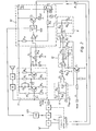
- An FM seek tuning receiver shown as a block diagram in FIG. 1 and equipped for stereo reception has an FM tuning part 1, a control circuit 2 for a seek seek tuning, an IF amplifier 3, an FM demodulator 4, a stereo decoder 5 and an NF- Amplifier 6 in a manner known per se.
- the output of the FM demodulator 4 is connected via a selective filter 7, whose pass frequency lies above the stereo multiplex signal and within the IF bandwidth, and via an electrical gate switch 8 to a first rectifier stage 9, which is controlled by an electronically controllable level adjuster 100 a level comparison stage 10 is connected downstream.
- the control input of the level adjuster 100 is connected to the IF amplifier 3 via a rectifier stage 101.
- the output of the FM demodulator 4 is also connected via an LF bandpass filter 11 to a second rectifier stage 12 which is designed as a peak rectifier and which actuates the electrical gate switch 8 with its output signal.
- the output and a further input of the level comparison stage 10 are connected via lines A and B to the control circuit 2 for the station search.
- the output of the amplifier serving as a selective filter 7 is connected via a capacitor C4 to the inverting input of a first operational amplifier VI connected via a resistor R7 to a positive reference voltage source U ref .
- the output of the operational amplifier Vl additionally serving as a gate circuit 8 is connected to the anode of a diode D1, the cathode of which is connected via a resistor R8 to a charging capacitor C5 which is connected to ground and to which a resistor R9 is connected in parallel.
- the connected to the resistors R8, R9 of the integrator capacitor C5 is connected to the inverting input of a second operational amplifier V2, which together with a downstream transistor T3, an indicator lamp La and an adjustable voltage divider Rx, the tap via a resistor R10 is connected to the non-inverting input of operational amplifier V2, which forms level comparison stage 10.
- the capacitors C6, C7 and resistors R11, R12 forming the LF bandpass 11 are dimensioned such that the LF bandpass 11 has a passband of approximately 200 to 5000 Hz.
- the output terminals of the LF bandpass are connected to the inputs of a third operational amplifier V3, the inverting input being connected to the reference voltage source U ref .
- the output of the third operational amplifier V3 is connected via a capacitor C8 to the non-inverting input of a fourth operational amplifier V4, which is connected to ground via a resistor R13, the inverting input of which is connected to the collector of a transistor T4 connected to the emitter.
- the output of the fourth operational amplifier V4 is connected to the anode of a diode D2, which also has its cathode at the inverting input.
- the cathode of the diode D2, which is connected to ground via a capacitor C9, is connected via a resistor R14 to the non-inverting input of the first operational amplifier V1 provided as gate switch 8 via a resistor R15.
- a rectifier arrangement designed as a voltage doubler circuit which consists of diodes D3, D4, capacitors C10, CI1 and a resistor R16, is connected to the output of the selective filter 7, which is designed as an amplifier.
- the diodes D3, D4 of the rectifier arrangement are polarized in such a way that a voltage arising at their output is negatively directed.
- the output of the rectifier arrangement is connected via resistor R16 to the non-inverting input of the second operational amplifier V2 connected via a resistor R17 to a positive operating voltage source + UB, the output of which is connected via an electronically controllable level adjuster 100 to the base of transistor T3.
- the control input of the level adjuster 100 is connected to the IF amplifier 3 via a rectifier stage 101.
- a particularly simple embodiment of the controllable level adjuster 100 is shown in FIG. 3.
- the level adjuster 100 essentially has an ohmic voltage divider R100 / R101 and a diode D100.
- interference pulses also occur at the output of the FM demodulator 4 above the multiplex signal range, i.e. above 53 kHz.
- the selective filter 7 having an amplifier, the interference components in the range of 150 kHz are preferably detected and amplified.
- the interference components now pass through the capacitor C4, the first operational amplifier VI, to the first rectifier stage 9, which charges the charging capacitor C5.
- the level of the voltage across this capacitor C5 is already a measure of the size of the interference components and of the reception quality of the received signal.
- an LF frequency component of the signal present at the output of the FM demodulator is conducted via the LF bandpass 11 and the third operational amplifier V3 of the second rectifier stage 12, which is designed as a peak rectifier.
- the DC voltage signal present at the capacitor C9 provides information as to whether an LF modulation signal is present or not.
- the reset time constant for a failure of the LF modulation is determined by the dimensioning of the resistors R14, R15 and the capacitor C9. At the start of each measurement, a reset pulse can be used to query the current LF reproduction via the control input of the transistor T4.
- a diode voltage from the diode D2 reaches the non-inverting input of the operational amplifier V1, which amplifies the interference signals fed to it via the capacitor C4.
- the amplified interference signals rectified by means of the diode D1 are fed to the charging capacitor C5 and integrated according to frequency, frequency and amplitude.
- the integration time which is decisive for the measuring time, is determined by the resulting resistance value of the resistors R9, RIO acting in parallel. The more frequent or persistent interference signals occur, the higher the DC voltage at capacitor C5.
- the charging voltage of C5 and the DC voltage tapped at the adjustable voltage divider Rx are fed to the inverting input of the second operational amplifier V2.
- the charging capacitor C5 In the event of a high degree of interference of the received signal, the charging capacitor C5 is charged to a maximum; a small DC voltage is to be adjusted via the voltage divider Rx for interference comparison in order to cause the output status of the operational amplifier V2 to topple over and thus the transistor T3 to switch through and the indicator lamp La to light up. If there are no faults, the charging capacitor C5 is not charged.
- the voltage divider Rx must be regulated to a maximum DC voltage. This makes it possible to evaluate the degree of interference by evaluating the reference voltage set with the voltage divider Rx.
- a carrier rectification using diodes D3, D4 generates a negative DC voltage, which is fed into the base of the voltage divider formed from resistors R16, R17 .
- the operating point of the second operational amplifier V2 is shifted and an addition of the. possible disturbance variables, which can also be assessed via the size of the voltage set on the voltage divider Rx.
- the level comparison stage 10 is given 2 different level values via the line A by the control circuit for station search 2.
- the control circuit 2 is informed via line B that the level is below or above a predetermined level by a level of the actual value. It is thus possible not only to compare the interference levels of two transmitters received simultaneously with separate receiver trains, but also to store the interference level values of previously received transmitters and to use these as setpoints for a level comparison when a transmitter is received. However, it is also readily possible to use only the voltages occurring at the capacitors C5 and / or Cll for the assessment of a fault.
- the measurement variable of the reception quality which can be gathered from the level comparison stage 10 would run approximately as a function of the field strength according to curve a in FIG. 4.
- the limit of the IF amplifier 3 is left in the lower field strength range and the useful signal decreases faster than the interference signal, the quality measure is distorted to an apparently good quality in this area.
- the measured variable of the reception quality is influenced in such a way that the measured variable according to FIG. 4, curve b, decreases with a decreasing field strength below a predetermined low RF input level P.
- the measurement variable for the field strength required to control the electronically adjustable level adjuster 100 can be obtained from the IF stage 3 in a manner known per se via a rectifier stage 101.
- the FM demodulator 4 can also be used to obtain the measured variable for the field strength.
Landscapes
- Engineering & Computer Science (AREA)
- Computer Hardware Design (AREA)
- Microelectronics & Electronic Packaging (AREA)
- Circuits Of Receivers In General (AREA)
- Monitoring And Testing Of Transmission In General (AREA)
- Stereo-Broadcasting Methods (AREA)
- Noise Elimination (AREA)
- Radio Transmission System (AREA)
Priority Applications (1)
| Application Number | Priority Date | Filing Date | Title |
|---|---|---|---|
| AT82103928T ATE13117T1 (de) | 1981-09-26 | 1982-05-06 | Schaltungsanordnung zur ermittlung der empfangsqualitaet fuer einen fm-empfaenger. |
Applications Claiming Priority (2)
| Application Number | Priority Date | Filing Date | Title |
|---|---|---|---|
| DE3138395 | 1981-09-26 | ||
| DE19813138395 DE3138395A1 (de) | 1981-09-26 | 1981-09-26 | Schaltungsanordnung zur ermittlung der empfangsqualitaet fuer einen fm-empfaenger |
Publications (2)
| Publication Number | Publication Date |
|---|---|
| EP0075647A1 true EP0075647A1 (fr) | 1983-04-06 |
| EP0075647B1 EP0075647B1 (fr) | 1985-05-02 |
Family
ID=6142713
Family Applications (1)
| Application Number | Title | Priority Date | Filing Date |
|---|---|---|---|
| EP82103928A Expired EP0075647B1 (fr) | 1981-09-26 | 1982-05-06 | Circuit pour déterminer la qualité de réception d'un récepteur FM |
Country Status (4)
| Country | Link |
|---|---|
| EP (1) | EP0075647B1 (fr) |
| JP (1) | JPS5870654A (fr) |
| AT (1) | ATE13117T1 (fr) |
| DE (1) | DE3138395A1 (fr) |
Cited By (3)
| Publication number | Priority date | Publication date | Assignee | Title |
|---|---|---|---|---|
| EP0132752A2 (fr) * | 1983-07-20 | 1985-02-13 | Hans Kolbe & Co. | Détecteur pour l'indication des pointes de déviation de fréquence parasitaire |
| EP0430468A2 (fr) * | 1989-11-30 | 1991-06-05 | Ford Motor Company Limited | Circuit d'indication du rapport signal-bruit pour récepteurs FM |
| CN1110913C (zh) * | 1997-07-16 | 2003-06-04 | 日本胜利株式会社 | 正交频分多路复用信号的分集接收装置 |
Families Citing this family (1)
| Publication number | Priority date | Publication date | Assignee | Title |
|---|---|---|---|---|
| DE3718845A1 (de) * | 1987-06-05 | 1988-12-15 | Thomson Brandt Gmbh | Empfangsgeraet fuer rundfunksignale mit einer darin enthaltenen zusaetzlichen information (rds) |
Citations (4)
| Publication number | Priority date | Publication date | Assignee | Title |
|---|---|---|---|---|
| US3448385A (en) * | 1965-06-28 | 1969-06-03 | Scott Inc H H | Stereophonic receiver squelch apparatus |
| DE1591144A1 (de) * | 1967-11-28 | 1970-07-16 | Dietrich Gottstein | Empfangseinrichtung mit Suchautomatik,insbesondere fuer UKW-Rundfunkempfang im Kraftfahrzeug |
| DE2345649A1 (de) * | 1973-09-11 | 1975-03-20 | Philips Patentverwaltung | Schaltungsanordnung zur automatischen sendersuche |
| DE2840533A1 (de) * | 1978-09-18 | 1980-03-27 | Hans Ing Grad Wellhausen | Rundfunk- oder fernsehempfaenger |
Family Cites Families (1)
| Publication number | Priority date | Publication date | Assignee | Title |
|---|---|---|---|---|
| DE3126224A1 (de) * | 1981-07-03 | 1983-01-20 | Blaupunkt-Werke Gmbh, 3200 Hildesheim | Schaltungsanordnung zur ermittlung der empfangsqualitaet fuer einen fm-empfaenger |
-
1981
- 1981-09-26 DE DE19813138395 patent/DE3138395A1/de active Granted
-
1982
- 1982-05-06 EP EP82103928A patent/EP0075647B1/fr not_active Expired
- 1982-05-06 AT AT82103928T patent/ATE13117T1/de not_active IP Right Cessation
- 1982-09-27 JP JP57166766A patent/JPS5870654A/ja active Granted
Patent Citations (4)
| Publication number | Priority date | Publication date | Assignee | Title |
|---|---|---|---|---|
| US3448385A (en) * | 1965-06-28 | 1969-06-03 | Scott Inc H H | Stereophonic receiver squelch apparatus |
| DE1591144A1 (de) * | 1967-11-28 | 1970-07-16 | Dietrich Gottstein | Empfangseinrichtung mit Suchautomatik,insbesondere fuer UKW-Rundfunkempfang im Kraftfahrzeug |
| DE2345649A1 (de) * | 1973-09-11 | 1975-03-20 | Philips Patentverwaltung | Schaltungsanordnung zur automatischen sendersuche |
| DE2840533A1 (de) * | 1978-09-18 | 1980-03-27 | Hans Ing Grad Wellhausen | Rundfunk- oder fernsehempfaenger |
Non-Patent Citations (1)
| Title |
|---|
| ELEKTOR, Band 2, Nr. 7-8, Juli-August 1976, Canterbury (GB) * |
Cited By (5)
| Publication number | Priority date | Publication date | Assignee | Title |
|---|---|---|---|---|
| EP0132752A2 (fr) * | 1983-07-20 | 1985-02-13 | Hans Kolbe & Co. | Détecteur pour l'indication des pointes de déviation de fréquence parasitaire |
| EP0132752A3 (en) * | 1983-07-20 | 1986-01-08 | Hans Kolbe & Co. | Detector for the indication of parasitic frequency deviation peaks |
| EP0430468A2 (fr) * | 1989-11-30 | 1991-06-05 | Ford Motor Company Limited | Circuit d'indication du rapport signal-bruit pour récepteurs FM |
| EP0430468A3 (en) * | 1989-11-30 | 1992-05-20 | Ford Motor Company Limited | Signal-to-noise ratio indicating circuit for fm receivers |
| CN1110913C (zh) * | 1997-07-16 | 2003-06-04 | 日本胜利株式会社 | 正交频分多路复用信号的分集接收装置 |
Also Published As
| Publication number | Publication date |
|---|---|
| ATE13117T1 (de) | 1985-05-15 |
| DE3138395C2 (fr) | 1990-05-23 |
| EP0075647B1 (fr) | 1985-05-02 |
| DE3138395A1 (de) | 1983-04-28 |
| JPH0210616B2 (fr) | 1990-03-08 |
| JPS5870654A (ja) | 1983-04-27 |
Similar Documents
| Publication | Publication Date | Title |
|---|---|---|
| DE3590049T1 (de) | Diversity-Verfahren und Einrichtung vom Umschalttyp für FM-Empfänger | |
| DE3107970C2 (de) | FM-Empfänger mit wenigstens zwei Antennen | |
| DE3447282C2 (fr) | ||
| EP0069214B1 (fr) | Circuit pour déterminer la qualité de réception d'un récepteur FM | |
| DE2646256A1 (de) | Signalqualitaetsdetektor | |
| DE843559C (de) | Demodulator fuer frequenzmodulierte Traegerwellen | |
| EP0417150A1 (fr) | Element de reception radio fm. | |
| DE3721918C1 (en) | Method for evaluating the suitability for reception of the frequency-modulated broadcast transmissions received in an FM broadcast receiver, and circuit arrangement for carrying out the method | |
| EP0075647B1 (fr) | Circuit pour déterminer la qualité de réception d'un récepteur FM | |
| EP0417148B1 (fr) | Element de reception radio fm | |
| DE2909520B2 (fr) | ||
| WO1994009584A1 (fr) | Procede permettant de determiner un canal libre dans des systemes de transmission radio mrf | |
| EP0995281B1 (fr) | Circuit de reception de donnees pour signaux infrarouges | |
| EP0418270B1 (fr) | Element de reception radio fm | |
| EP0417149A1 (fr) | Element de reception radio fm. | |
| DE4338700C2 (de) | Schaltungsanordnung zum Erkennen von Nachbarkanalstörungen in einem Stereo-Multiplex-Rundfunkempfänger | |
| DE2922011C2 (de) | Einrichtung zum Detektieren von impulsförmigen Störsignalen | |
| DE2902616C3 (de) | UKW-Empfänger, insbesondere Autoempfänger, mit feldstärkeabhängiger Lautstärkesteuerung | |
| DE3148085C2 (fr) | ||
| EP0411485B1 (fr) | Procédé pour détecter des distortions multivoies lors de la réception radio à modulation de fréquence, et montage pour réaliser ce procédé | |
| DE19722385C2 (de) | Verfahren zur Erkennung von Multipathstörungen beim FM-Rundfunkempfang und Schaltungsanordnung zur Durchführung des Verfahrens | |
| DE2827572B1 (de) | Verfahren zur Stoerbeseitigung in einer mobilen Rundfunkempfangsanlage | |
| DE3240854C2 (de) | FM-Empfänger mit einem Ratiodetektor mit Siliziumdioden | |
| DE3938717A1 (de) | Verfahren und schaltung zum umschalten zwischen den frequenzmodulierten hf-signalen von mindestens zwei empfangs-antennen | |
| DE3217447C2 (fr) |
Legal Events
| Date | Code | Title | Description |
|---|---|---|---|
| PUAI | Public reference made under article 153(3) epc to a published international application that has entered the european phase |
Free format text: ORIGINAL CODE: 0009012 |
|
| AK | Designated contracting states |
Designated state(s): AT FR GB IT |
|
| 17P | Request for examination filed |
Effective date: 19830915 |
|
| ITF | It: translation for a ep patent filed |
Owner name: STUDIO JAUMANN |
|
| GRAA | (expected) grant |
Free format text: ORIGINAL CODE: 0009210 |
|
| AK | Designated contracting states |
Designated state(s): AT FR GB IT |
|
| REF | Corresponds to: |
Ref document number: 13117 Country of ref document: AT Date of ref document: 19850515 Kind code of ref document: T |
|
| ET | Fr: translation filed | ||
| PLBE | No opposition filed within time limit |
Free format text: ORIGINAL CODE: 0009261 |
|
| STAA | Information on the status of an ep patent application or granted ep patent |
Free format text: STATUS: NO OPPOSITION FILED WITHIN TIME LIMIT |
|
| 26N | No opposition filed | ||
| ITTA | It: last paid annual fee | ||
| PGFP | Annual fee paid to national office [announced via postgrant information from national office to epo] |
Ref country code: AT Payment date: 19930329 Year of fee payment: 12 |
|
| PGFP | Annual fee paid to national office [announced via postgrant information from national office to epo] |
Ref country code: GB Payment date: 19930423 Year of fee payment: 12 |
|
| PGFP | Annual fee paid to national office [announced via postgrant information from national office to epo] |
Ref country code: FR Payment date: 19930526 Year of fee payment: 12 |
|
| PG25 | Lapsed in a contracting state [announced via postgrant information from national office to epo] |
Ref country code: GB Effective date: 19940506 Ref country code: AT Effective date: 19940506 |
|
| GBPC | Gb: european patent ceased through non-payment of renewal fee |
Effective date: 19940506 |
|
| PG25 | Lapsed in a contracting state [announced via postgrant information from national office to epo] |
Ref country code: FR Effective date: 19950131 |
|
| REG | Reference to a national code |
Ref country code: FR Ref legal event code: ST |