EP0075295B1 - Système de transmission optique pour signaux numériques à haute fréquence - Google Patents
Système de transmission optique pour signaux numériques à haute fréquence Download PDFInfo
- Publication number
- EP0075295B1 EP0075295B1 EP82108608A EP82108608A EP0075295B1 EP 0075295 B1 EP0075295 B1 EP 0075295B1 EP 82108608 A EP82108608 A EP 82108608A EP 82108608 A EP82108608 A EP 82108608A EP 0075295 B1 EP0075295 B1 EP 0075295B1
- Authority
- EP
- European Patent Office
- Prior art keywords
- signal
- laser diode
- modulation
- current
- frequency
- Prior art date
- Legal status (The legal status is an assumption and is not a legal conclusion. Google has not performed a legal analysis and makes no representation as to the accuracy of the status listed.)
- Expired
Links
- 230000005540 biological transmission Effects 0.000 title claims abstract description 29
- 230000003287 optical effect Effects 0.000 title claims abstract description 24
- 230000010355 oscillation Effects 0.000 claims description 4
- 238000012545 processing Methods 0.000 claims description 3
- 230000008878 coupling Effects 0.000 claims 1
- 238000010168 coupling process Methods 0.000 claims 1
- 238000005859 coupling reaction Methods 0.000 claims 1
- 239000004020 conductor Substances 0.000 abstract 2
- 238000010586 diagram Methods 0.000 description 6
- 238000000034 method Methods 0.000 description 3
- 230000001105 regulatory effect Effects 0.000 description 3
- 230000003321 amplification Effects 0.000 description 2
- 238000004891 communication Methods 0.000 description 2
- 238000012544 monitoring process Methods 0.000 description 2
- 238000003199 nucleic acid amplification method Methods 0.000 description 2
- 230000000737 periodic effect Effects 0.000 description 2
- 230000035945 sensitivity Effects 0.000 description 2
- RYGMFSIKBFXOCR-UHFFFAOYSA-N Copper Chemical compound [Cu] RYGMFSIKBFXOCR-UHFFFAOYSA-N 0.000 description 1
- 238000013459 approach Methods 0.000 description 1
- 239000003990 capacitor Substances 0.000 description 1
- 238000006243 chemical reaction Methods 0.000 description 1
- 238000005352 clarification Methods 0.000 description 1
- 229910052802 copper Inorganic materials 0.000 description 1
- 239000010949 copper Substances 0.000 description 1
- 230000003247 decreasing effect Effects 0.000 description 1
- 230000002452 interceptive effect Effects 0.000 description 1
- 239000000203 mixture Substances 0.000 description 1
- 230000000717 retained effect Effects 0.000 description 1
- 238000007493 shaping process Methods 0.000 description 1
- 238000001228 spectrum Methods 0.000 description 1
Images


Classifications
-
- H—ELECTRICITY
- H04—ELECTRIC COMMUNICATION TECHNIQUE
- H04B—TRANSMISSION
- H04B17/00—Monitoring; Testing
- H04B17/0082—Monitoring; Testing using service channels; using auxiliary channels
- H04B17/0087—Monitoring; Testing using service channels; using auxiliary channels using auxiliary channels or channel simulators
-
- H—ELECTRICITY
- H04—ELECTRIC COMMUNICATION TECHNIQUE
- H04B—TRANSMISSION
- H04B10/00—Transmission systems employing electromagnetic waves other than radio-waves, e.g. infrared, visible or ultraviolet light, or employing corpuscular radiation, e.g. quantum communication
- H04B10/50—Transmitters
- H04B10/501—Structural aspects
- H04B10/503—Laser transmitters
- H04B10/504—Laser transmitters using direct modulation
-
- H—ELECTRICITY
- H04—ELECTRIC COMMUNICATION TECHNIQUE
- H04B—TRANSMISSION
- H04B10/00—Transmission systems employing electromagnetic waves other than radio-waves, e.g. infrared, visible or ultraviolet light, or employing corpuscular radiation, e.g. quantum communication
- H04B10/50—Transmitters
- H04B10/564—Power control
-
- H—ELECTRICITY
- H01—ELECTRIC ELEMENTS
- H01S—DEVICES USING THE PROCESS OF LIGHT AMPLIFICATION BY STIMULATED EMISSION OF RADIATION [LASER] TO AMPLIFY OR GENERATE LIGHT; DEVICES USING STIMULATED EMISSION OF ELECTROMAGNETIC RADIATION IN WAVE RANGES OTHER THAN OPTICAL
- H01S5/00—Semiconductor lasers
- H01S5/06—Arrangements for controlling the laser output parameters, e.g. by operating on the active medium
- H01S5/068—Stabilisation of laser output parameters
- H01S5/0683—Stabilisation of laser output parameters by monitoring the optical output parameters
- H01S5/06832—Stabilising during amplitude modulation
Definitions
- the invention relates to an optical transmission system for high-frequency digital signals with a laser diode transmitter, which contains a regulation of the laser diode bias current and / or the modulation current by converting a branched part of the useful light emitted by the laser diode into an electrical signal, with a receiver having a light-sensitive electrical component contains with a downstream amplifier and a signal processing device, and with a device for transmitting an additional low-frequency signal in which this is modulated onto another signal.
- Transmission systems for digital signals require remotely fed intermediate points inserted into the transmission path at certain intervals, in which the digital signals are regenerated in terms of amplitude and time.
- the remote feed current and also additional signals for example from a service channel or from an alarm and message channel, via the communication cable.
- additional signals for example from a service channel or from an alarm and message channel
- optical transmission systems there is occasionally the possibility of transmitting such additional signals via an additional remote feed line.
- regenerators for the optical transmission system With regard to the local supply of regenerators for the optical transmission system, however, the case may arise that no remote feed line is provided parallel to the entire optical transmission path. In this case, there is a need for an additional signal path, which is comparatively low in frequency compared to the digital signals, and which also runs via the optical transmission system.
- An electronic transmission system is known from Electronic Letters dated July 31, 1980, pages 624 to 626, in which an additional channel is provided for the transmission of monitoring information and as a service channel.
- the additional information is transmitted by directly modulating the bit rate of the transmitted data signals. This modulation causes an increase in the jitter, that is to say the phase modulation of the digital signals, which, possibly in conjunction with further interfering influences, can lead to interference in the transmission of the digital signals.
- a transmitter for an optical communication system which contains a regulation of the light source used by converting a branched part of the emitted useful light into an electrical signal and comparing this signal with a reference value.
- the additional signal can be superimposed on the reference signal used for the control, which results in a corresponding fluctuation of the light source bias current and thus a modulation of the envelope of the emitted light.
- the additional signal can be recovered from the fluctuation of the envelope, but this results in a high sensitivity to low-frequency interference, and the use of PIN-FET receivers with high impedance is also not possible because of their sensitivity to low-frequency components in the signal spectrum.
- DE-OS 2 841 433 discloses a method for regulating the bias current supplied to the laser diodes, in which a periodic oscillation with a frequency and frequency that is comparatively low compared to the transmission signal is superimposed on the bias current. Part of the light emitted by the laser diode is branched off, the periodic oscillation is recovered and, after shaping and comparison with a standard signal, is used for bias current control.
- DE-OS 2 847182 discloses a regulation of the modulation current of laser diodes corresponding to the bias current regulation.
- a further circuit arrangement for regulating the laser threshold value is known from “Electronic Letters” of November 23, 1978, pages 775 and 776, in which at least one low-frequency signal of small amplitude is also superimposed on the laser bias and the data signal to be transmitted.
- part of the light emitted by the laser diode is picked up by a photodiode, the low-frequency signal is recovered and, after appropriate conversion, is used to regulate the laser diode bias current and to regulate the modulation current.
- a transmission of these control signals via the optical transmission system is not considered in the prior art, particularly with regard to the very low amplitudes of the control signal.
- the object of the invention is therefore to create a possibility for setting up a monitoring or service channel which has as little influence as possible on the digital signals to be transmitted and does not require the use of additional line devices.
- a particular advantage is that the control devices of the laser diode transmitter can be used to transmit the additional signal, and therefore the additional effort required is comparatively very low. Nevertheless, the transmission of the additional signal is independent of the control processes of the laser diode transmitter, so that the additional signal is falsified by control deviations can be closed.
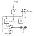
- the laser transmitter shown in FIG. 1 contains two control loops which are used to control the modulation current and the laser diode bias current.
- a laser diode LD optically couples a photodiode FD to the laser diode. After amplification of the photodiode output signal in a conventional amplifier (not shown in the drawing), this signal reaches the input of a first comparator V1, which is constructed in the manner of a differential amplifier. The output signal of the photodiode is applied to the inverting input of this amplifier, while a first reference voltage Ur1 is connected to the non-inverting input.
- the inverting input and output of the amplifier are capacitively connected to each other, the control input of a source QO for the laser diode bias is connected to the output.
- the output of the source for the laser diode bias current is connected directly to a connection of the laser diode LD.
- This control loop regulates the mean light output of the laser diode, deviations from the setpoint are determined and amplified in comparator V1 and continue to track the bias current of the laser diode until the setpoint is reached.
- a second control loop is provided, which is also connected to the photodiode.
- a first mixer M1 is provided, one input of which is connected to a connection of the photodiode FD and the other input of which is connected to a connection of a modulator and oscillator FMO.
- This oscillator generates an oscillation which is very low in frequency compared to the digital signals and is emitted to the first mixer M1 and to an input of a second mixer M2.
- the inverting input of a second comparator V2 is connected to the output of the first mixer, which is constructed analogously to the first comparator in the form of a differential amplifier and to the other connection of which a second reference voltage Ur2 is applied.
- This second comparator V2 is connected to a control input of a source QM for the modulation current, the output of which is connected to a second input of the second mixer M2.
- the output of this second mixer is connected in parallel to the output of the source QO for the laser diode bias to the laser diode.
- FIG. 2 serves to explain the known conditions in the modulation current control of laser diodes by means of a low-frequency control signal of small amplitude.
- the characteristic curve of a laser diode that is, the emitted light power P as a function of the diode current I, is shown at the top left.
- the lower limit of the laser diode control is given by the power PO, which marks the first kink of the characteristic curve, while the upper limit - approximately the second kink - that is the maximum light output that can be emitted by the laser diode in continuous operation at P1.
- Currents supplied to the laser diode are shown below the characteristic curve of the laser diode.
- the laser diode bias current is denoted by 10 and the laser diode modulation current by Imod.
- control signals ISO and IS1 are shown, one of which is superimposed on the modulation current at the lower limit and the other at the upper limit.
- the superimposition takes place in the second modulator M2, the period of the low-frequency signal Ts fed to this modulator is retained during the superimposition.
- the light output emitted by the laser diode is shown to the right of the laser diode characteristic.
- the two parts of the control signal result in light powers PSO and PS1, which fluctuate around the laser diode quiescent power PO and the maximum modulation P1.
- the control signal contained in the light signal is recorded via the photodiode FD in accordance with FIG. 1 and fed to the mixer M1.
- the output signal of the mixer M1 is compared in the second comparator V2 with the second reference voltage Ur2 and the resulting DC voltage after amplification is used to control the source QM for the modulation current.
- the difference PS1 - PSO is used for control, the control then consists in that this difference remains constant.
- the second part Is1 of the control signal can be omitted.
- the amplitude of the light power PSO is fed to the second comparator V2.
- the regulation then takes place in such a way that the light output PSO remains constant, since if the light output PSO is too high, the operating point moves to a higher value and if the light output PSO is too low, it approaches one low value is shifted.
- 3a shows this telemetry data in the form of a 6-bit NRZ-PCM word.
- the light P emitted by the laser diode is shown in FIG. 3d. It can be seen that the two components PS1 and PSO of the control signal have approximately the same amplitude. After the difference has been formed, the control signal then disappears, so that there is no manipulated variable for changing the modulation signal emitted by the source QM - the control is thus in the steady state.
- the proportions of the control signal are shown in FIGS. 2 and 3 enlarged compared to the modulation current for clarification; in practice, the amplitude of the control signal is at least a power of ten less than that of the modulation signal.
- the light emitted by the laser diode to the transmission path contains the control signal modulated with telemetry data.
- the optical receiver shown in FIG. 4 receives the transmitted light from an avalanche photodiode APD at the end of the optical waveguide and converts it into a corresponding electrical current which is amplified in a photodiode amplifier V3 specially adapted to the photodiode.
- a clock circuit TK for generating the bit clock of the transmitted digital signal, a pulse regenerator and a receiver for the modulated control signal are connected to the output of this amplifier via isolating amplifiers V4, V5, V6.
- the clock circuit TK and the pulse regenerator with amplitude decider AE and time decider ZE correspond to conventional devices connected via copper cables for digital signals with a comparable bit rate.
- the receiver for the modulated control signal contains a rectifier GR on the input side and then an RC element for peak value rectification.
- the time constant of the peak value rectification is dimensioned such that it can follow the low-frequency control signal, but not the higher-frequency useful signal.
- An FM demodulator FMDM follows the rectification, and the telemetry data is available at its output for further processing.
- the received light power with the two parts of the modulated control signal according to FIG. 3d is shown in the pulse diagram according to FIG. 5a.
- the voltage curve shown in FIG. 5b results on capacitor C, which shows the modulated control signal together with a DC component.
- the signal curve shown in FIG. 5c results, which corresponds to the telemetry signal according to FIG. 3a.
- a low-pass filter is included in the receiver instead of the peak value rectification. In view of the large frequency spacing between the control signal and the useful signal in the present case, such a low-pass filter can be easily implemented.
Landscapes
- Physics & Mathematics (AREA)
- Electromagnetism (AREA)
- Engineering & Computer Science (AREA)
- Computer Networks & Wireless Communication (AREA)
- Signal Processing (AREA)
- Optics & Photonics (AREA)
- Optical Communication System (AREA)
- Monitoring And Testing Of Transmission In General (AREA)
- Dc Digital Transmission (AREA)
Claims (4)
caractérisé par le fait,
Priority Applications (1)
| Application Number | Priority Date | Filing Date | Title |
|---|---|---|---|
| AT82108608T ATE24641T1 (de) | 1981-09-21 | 1982-09-17 | Optisches uebertragungssystem fuer hochfrequente digitale signale. |
Applications Claiming Priority (2)
| Application Number | Priority Date | Filing Date | Title |
|---|---|---|---|
| DE3137497 | 1981-09-21 | ||
| DE19813137497 DE3137497A1 (de) | 1981-09-21 | 1981-09-21 | Optisches uebertragungssystem fuer hochfrequente digitale signale |
Publications (3)
| Publication Number | Publication Date |
|---|---|
| EP0075295A2 EP0075295A2 (fr) | 1983-03-30 |
| EP0075295A3 EP0075295A3 (en) | 1984-08-01 |
| EP0075295B1 true EP0075295B1 (fr) | 1986-12-30 |
Family
ID=6142235
Family Applications (1)
| Application Number | Title | Priority Date | Filing Date |
|---|---|---|---|
| EP82108608A Expired EP0075295B1 (fr) | 1981-09-21 | 1982-09-17 | Système de transmission optique pour signaux numériques à haute fréquence |
Country Status (5)
| Country | Link |
|---|---|
| US (1) | US4471494A (fr) |
| EP (1) | EP0075295B1 (fr) |
| JP (1) | JPS6046579B2 (fr) |
| AT (1) | ATE24641T1 (fr) |
| DE (2) | DE3137497A1 (fr) |
Families Citing this family (37)
| Publication number | Priority date | Publication date | Assignee | Title |
|---|---|---|---|---|
| NL8200002A (nl) * | 1982-01-04 | 1983-08-01 | Philips Nv | Foutlocalisatie-inrichting voor digitaal optische transmissiesysteem. |
| DE3333248A1 (de) * | 1983-09-14 | 1985-03-28 | Siemens Ag | Laserregelung fuer optische uebertragungssysteme |
| DE3333247A1 (de) * | 1983-09-14 | 1985-03-28 | Siemens Ag | Optisches uebertragungssystem mit laserregelung |
| JPS61201222A (ja) * | 1985-03-04 | 1986-09-05 | Hitachi Ltd | 光パルス増幅整形装置 |
| GB2175480B (en) * | 1985-05-21 | 1988-12-29 | Stc Plc | Demodulation of auxiliary low frequency channels in digital transmission systems |
| US4733398A (en) * | 1985-09-30 | 1988-03-22 | Kabushiki Kaisha Tohsiba | Apparatus for stabilizing the optical output power of a semiconductor laser |
| DE3544393A1 (de) * | 1985-12-16 | 1987-06-19 | Philips Patentverwaltung | Diensteintegrierendes, digitales nachrichtenuebertragungssystem mit einrichtungen zur gemeinsamen uebertragung von schmalband- und breitbandsignalen |
| DE59008778D1 (de) * | 1989-01-17 | 1995-05-04 | Siemens Ag | Laserdiodensender mit Schutz- und Alarmierungsschaltung. |
| EP0386736B1 (fr) * | 1989-03-09 | 1995-06-07 | Canon Kabushiki Kaisha | Système de communication optique |
| US5091797A (en) * | 1989-11-13 | 1992-02-25 | Siemens Aktiengesellschaft | Method and apparatus for modulation current regulation for laser diodes |
| DE69127840T2 (de) * | 1990-03-01 | 1998-03-05 | Fujitsu Ltd | Optischer Sender |
| USRE36088E (en) * | 1990-03-01 | 1999-02-09 | Fujitsu Limited | Optical transmitter |
| US5003624A (en) * | 1990-03-29 | 1991-03-26 | Hughes Aircraft Company | Automatic bias controller for electro-optic modulator |
| US4989212A (en) * | 1990-04-09 | 1991-01-29 | Trw, Inc. | Laser diode phase modulation technique |
| JP2527829B2 (ja) * | 1990-04-25 | 1996-08-28 | 三菱電機株式会社 | 光応用測定装置 |
| DE69123674T2 (de) * | 1990-09-17 | 1997-04-17 | Nippon Electric Co | Mobiles Kommunikationssystem |
| JPH04192729A (ja) * | 1990-11-27 | 1992-07-10 | Fujitsu Ltd | 光送信装置 |
| EP0512556B1 (fr) * | 1991-05-10 | 1997-09-03 | Nec Corporation | Emetteur et récepteur optique avec un seul module optique |
| US5390185A (en) * | 1992-10-09 | 1995-02-14 | U.S. Philips Corporation | Transmission system for a combination of a main signal and an auxiliary signal |
| EP0592041A1 (fr) * | 1992-10-09 | 1994-04-13 | Koninklijke Philips Electronics N.V. | Système de transmission avec un canal principal et un canal auxiliaire |
| US5502298A (en) * | 1992-12-21 | 1996-03-26 | Ericsson Raynet | Apparatus and method for controlling an extinction ratio of a laser diode over temperature |
| US5448629A (en) * | 1993-10-14 | 1995-09-05 | At&T Corp. | Amplitude detection scheme for optical transmitter control |
| JPH07240555A (ja) * | 1994-02-25 | 1995-09-12 | Fujitsu Ltd | 自動バイアス電流制御型apc回路を有する光送信器 |
| JPH0818510A (ja) * | 1994-07-01 | 1996-01-19 | Fujitsu Ltd | 光通信モジュール |
| US5463648A (en) * | 1994-08-01 | 1995-10-31 | Litton Systems, Inc. | Pulse forming network for diode laser |
| US6271942B1 (en) * | 1996-11-26 | 2001-08-07 | Matsushita Electric Industrial Co., Ltd. | Optical transmission device and system |
| DE19736695A1 (de) * | 1997-08-22 | 1999-03-18 | Siemens Ag | Verfahren und Anordnung zum Übertragen eines mit einem Zusatzsignal modulierten optischen Datensignals über nicht transparente Funktionseinheiten |
| DE69820393T2 (de) * | 1997-10-28 | 2004-10-07 | Broadband Royalty Corp | Optischer Sender zur Rauschimpulsverringerung in einer faseroptischen Verbindung |
| US6549310B1 (en) * | 1999-01-08 | 2003-04-15 | International Business Machines Corporation | Fiber optic data link module with built-in link diagnostics |
| US6678478B1 (en) * | 1999-06-01 | 2004-01-13 | Advantest Corporation | Correcting method of optical signal transmission system and optical signal transmission system using said correcting method |
| US6649898B1 (en) * | 2000-06-30 | 2003-11-18 | Intel Corporation | Method and apparatus for optically enabling a circuit component in a large scale integrated circuit |
| US7505498B2 (en) | 2002-01-08 | 2009-03-17 | Jorge Sanchez | Apparatus and method for measurement for dynamic laser signals |
| US7027685B2 (en) * | 2003-08-20 | 2006-04-11 | The Boeing Company | Apparatus and method for fiber optic link with built-in test |
| ATE489750T1 (de) * | 2004-04-21 | 2010-12-15 | Tecey Software Dev Kg Llc | Verfahren und vorrichtung für durch digitale signalverarbeitung verbesserte kompensation der laser-leistungsfähigkeit |
| US7706685B2 (en) * | 2005-09-20 | 2010-04-27 | Lockheed Martin Corporation | Data communication network using optical power averaged multiplexing |
| US7639001B2 (en) * | 2006-01-17 | 2009-12-29 | The Boeing Company | Built-in test for high speed electrical networks |
| US8385749B2 (en) * | 2009-07-02 | 2013-02-26 | International Business Machines Corporation | High speed optical transmitter with directly modulated laser source |
Family Cites Families (10)
| Publication number | Priority date | Publication date | Assignee | Title |
|---|---|---|---|---|
| DE2529479C3 (de) * | 1975-07-02 | 1979-12-06 | Licentia Patent-Verwaltungs-Gmbh, 6000 Frankfurt | Schaltungsanordnung zur Stabilisierung, insbesondere Temperaturstabilisierung, eines optischen Empfängers |
| JPS5269506A (en) * | 1975-12-08 | 1977-06-09 | Fujitsu Ltd | Secondary carrier wave piling pcm-im communication system |
| FR2361022A1 (fr) * | 1976-08-06 | 1978-03-03 | Aerospatiale | Procede et dispositif de transmission de signaux par fibres optiques |
| GB1565764A (en) * | 1978-02-02 | 1980-04-23 | Standard Telephones Cables Ltd | Optical fibre digital transmission systems |
| GB1582726A (en) * | 1978-05-31 | 1981-01-14 | Standard Telephones Cables Ltd | Avalanche photodetector demodulation |
| GB2025121B (en) * | 1978-07-06 | 1982-05-19 | Post Office | Stabilisation of injection lasers |
| DE2841433C2 (de) * | 1978-09-22 | 1983-08-25 | Siemens Ag, 1000 Berlin Und 8000 Muenchen | Vorstromregelung von Laserdioden |
| DE2847182C3 (de) * | 1978-10-30 | 1986-07-10 | Siemens Ag, 1000 Berlin Und 8000 Muenchen | Verfahren zur Modulationsstromregelung von Laserdioden |
| JPS5621434A (en) * | 1979-07-31 | 1981-02-27 | Fujitsu Ltd | Sessional monitor signal transmission system |
| DE2946701C2 (de) * | 1979-11-20 | 1985-09-19 | Standard Elektrik Lorenz Ag, 7000 Stuttgart | Schaltungsanordnung zur Regeneration von blockweise übertragenen Datenbits |
-
1981
- 1981-09-21 DE DE19813137497 patent/DE3137497A1/de not_active Withdrawn
-
1982
- 1982-08-12 US US06/407,586 patent/US4471494A/en not_active Expired - Fee Related
- 1982-09-17 DE DE8282108608T patent/DE3274941D1/de not_active Expired
- 1982-09-17 AT AT82108608T patent/ATE24641T1/de not_active IP Right Cessation
- 1982-09-17 EP EP82108608A patent/EP0075295B1/fr not_active Expired
- 1982-09-20 JP JP57162425A patent/JPS6046579B2/ja not_active Expired
Also Published As
| Publication number | Publication date |
|---|---|
| ATE24641T1 (de) | 1987-01-15 |
| EP0075295A2 (fr) | 1983-03-30 |
| JPS5862945A (ja) | 1983-04-14 |
| DE3137497A1 (de) | 1983-04-07 |
| US4471494A (en) | 1984-09-11 |
| JPS6046579B2 (ja) | 1985-10-16 |
| DE3274941D1 (en) | 1987-02-05 |
| EP0075295A3 (en) | 1984-08-01 |
Similar Documents
| Publication | Publication Date | Title |
|---|---|---|
| EP0075295B1 (fr) | Système de transmission optique pour signaux numériques à haute fréquence | |
| DE2902789C2 (fr) | ||
| DE3232430C2 (de) | Optisches Nachrichtenübertragungssystem | |
| DE69316461T2 (de) | Verfahren und Vorrichtung eines abstimmbaren Filters und optisches Kommunikationssystem unter Verwendung dieser Vorrichtung | |
| DE69304806T2 (de) | Laservorspannungs- und -modulationsschaltung | |
| DE69507372T2 (de) | Lasermodulationsregler unter Verwendung eines Additions- und eines Amplitudenmodulationssteuerungstones | |
| DE69406411T2 (de) | Vorrichtung und Verfahren zur Steuerung von Strom und Modulation eines Lasers | |
| DE69006370T2 (de) | Lasersteuerschaltung. | |
| DE69227749T2 (de) | Optische Sender | |
| DE2712292A1 (de) | Regenerator fuer ein optisches uebertragungs-system | |
| EP0227164A2 (fr) | Système de transmission à intégration de services d'informations numériques avec des dispositifs pour la transmission simultanée de signaux à large bande et à bande étroite | |
| EP0237922B1 (fr) | Procédé pour la régulation de la puissance optique d'un laser et circuit pour la mise en oeuvre de ce procédé | |
| EP0656700A1 (fr) | Système optique pour la transmission d'un signal à plusieurs étages | |
| DE2841433A1 (de) | Vorstromregelung von laserdioden | |
| DE69408759T2 (de) | Verfahren und Gerät zur Frequenzmodulation eines Halbleiterlasers und darauf beruhendes optisches Kommunikationssystem | |
| DE4040170A1 (de) | Uebertragungssignal | |
| DE4109683A1 (de) | System fuer optische signaluebertragung, insbesondere optisches kabelfernsehsystem, mit ueberwachungs- und dienstkanaleinrichtung | |
| DE3307309C2 (fr) | ||
| DE60126542T2 (de) | Optisches Übertragungssystem und optischer Empfänger | |
| DE1437169B2 (de) | Verfahren zur schnelluebertragung von daten im restseiten bandverfahren die nach einem binaeren vode oder nach einem mehrpegelcode verschluesselt sind | |
| EP0582275A1 (fr) | Méthode de génération d'un signal modulé en fréquence sans distorsion et dispositif pour la mise en oeuvre de ce procédé | |
| EP0428016B1 (fr) | Commande de courant de modulation pour diodes laser | |
| DE69024414T2 (de) | Selbstanpassender, analoger Laser-Sender | |
| DE3333247A1 (de) | Optisches uebertragungssystem mit laserregelung | |
| DE69431786T2 (de) | Übertragungsnetz mit Vielfachzugriff und Unterträger |
Legal Events
| Date | Code | Title | Description |
|---|---|---|---|
| PUAI | Public reference made under article 153(3) epc to a published international application that has entered the european phase |
Free format text: ORIGINAL CODE: 0009012 |
|
| AK | Designated contracting states |
Designated state(s): AT BE CH DE FR GB IT LI LU NL SE |
|
| PUAL | Search report despatched |
Free format text: ORIGINAL CODE: 0009013 |
|
| AK | Designated contracting states |
Designated state(s): AT BE CH DE FR GB IT LI LU NL SE |
|
| 17P | Request for examination filed |
Effective date: 19841128 |
|
| GRAA | (expected) grant |
Free format text: ORIGINAL CODE: 0009210 |
|
| AK | Designated contracting states |
Kind code of ref document: B1 Designated state(s): AT BE CH DE FR GB IT LI LU NL SE |
|
| REF | Corresponds to: |
Ref document number: 24641 Country of ref document: AT Date of ref document: 19870115 Kind code of ref document: T |
|
| PG25 | Lapsed in a contracting state [announced via postgrant information from national office to epo] |
Ref country code: SE Effective date: 19861231 |
|
| REF | Corresponds to: |
Ref document number: 3274941 Country of ref document: DE Date of ref document: 19870205 |
|
| ET | Fr: translation filed | ||
| ITF | It: translation for a ep patent filed | ||
| PG25 | Lapsed in a contracting state [announced via postgrant information from national office to epo] |
Ref country code: LU Free format text: LAPSE BECAUSE OF NON-PAYMENT OF DUE FEES Effective date: 19870930 |
|
| PGFP | Annual fee paid to national office [announced via postgrant information from national office to epo] |
Ref country code: NL Payment date: 19870930 Year of fee payment: 6 |
|
| PLBE | No opposition filed within time limit |
Free format text: ORIGINAL CODE: 0009261 |
|
| STAA | Information on the status of an ep patent application or granted ep patent |
Free format text: STATUS: NO OPPOSITION FILED WITHIN TIME LIMIT |
|
| 26N | No opposition filed | ||
| PGFP | Annual fee paid to national office [announced via postgrant information from national office to epo] |
Ref country code: AT Payment date: 19890825 Year of fee payment: 8 |
|
| PG25 | Lapsed in a contracting state [announced via postgrant information from national office to epo] |
Ref country code: GB Effective date: 19890917 |
|
| PGFP | Annual fee paid to national office [announced via postgrant information from national office to epo] |
Ref country code: BE Payment date: 19890919 Year of fee payment: 8 |
|
| PG25 | Lapsed in a contracting state [announced via postgrant information from national office to epo] |
Ref country code: NL Effective date: 19900401 |
|
| GBPC | Gb: european patent ceased through non-payment of renewal fee | ||
| NLV4 | Nl: lapsed or anulled due to non-payment of the annual fee | ||
| PG25 | Lapsed in a contracting state [announced via postgrant information from national office to epo] |
Ref country code: FR Effective date: 19900531 |
|
| REG | Reference to a national code |
Ref country code: FR Ref legal event code: ST |
|
| PG25 | Lapsed in a contracting state [announced via postgrant information from national office to epo] |
Ref country code: AT Effective date: 19900917 |
|
| PG25 | Lapsed in a contracting state [announced via postgrant information from national office to epo] |
Ref country code: BE Effective date: 19900930 |
|
| BERE | Be: lapsed |
Owner name: SIEMENS A.G. BERLIN UND MUNCHEN Effective date: 19900930 |
|
| PGFP | Annual fee paid to national office [announced via postgrant information from national office to epo] |
Ref country code: DE Payment date: 19931119 Year of fee payment: 12 |
|
| PGFP | Annual fee paid to national office [announced via postgrant information from national office to epo] |
Ref country code: CH Payment date: 19931215 Year of fee payment: 12 |
|
| PG25 | Lapsed in a contracting state [announced via postgrant information from national office to epo] |
Ref country code: LI Effective date: 19940930 Ref country code: CH Effective date: 19940930 |
|
| REG | Reference to a national code |
Ref country code: CH Ref legal event code: PL |
|
| PG25 | Lapsed in a contracting state [announced via postgrant information from national office to epo] |
Ref country code: DE Effective date: 19950601 |