EP0073130B2 - Verfahren zur Herstellung eines Nur-Lesespeichers vom Maskentyp - Google Patents
Verfahren zur Herstellung eines Nur-Lesespeichers vom Maskentyp Download PDFInfo
- Publication number
- EP0073130B2 EP0073130B2 EP82304312A EP82304312A EP0073130B2 EP 0073130 B2 EP0073130 B2 EP 0073130B2 EP 82304312 A EP82304312 A EP 82304312A EP 82304312 A EP82304312 A EP 82304312A EP 0073130 B2 EP0073130 B2 EP 0073130B2
- Authority
- EP
- European Patent Office
- Prior art keywords
- forming
- mos transistors
- film
- semiconductor substrate
- source
- Prior art date
- Legal status (The legal status is an assumption and is not a legal conclusion. Google has not performed a legal analysis and makes no representation as to the accuracy of the status listed.)
- Expired - Lifetime
Links
Images


Classifications
-
- H10P30/204—
-
- H—ELECTRICITY
- H10—SEMICONDUCTOR DEVICES; ELECTRIC SOLID-STATE DEVICES NOT OTHERWISE PROVIDED FOR
- H10B—ELECTRONIC MEMORY DEVICES
- H10B20/00—Read-only memory [ROM] devices
- H10B20/27—ROM only
- H10B20/30—ROM only having the source region and the drain region on the same level, e.g. lateral transistors
- H10B20/38—Doping programmed, e.g. mask ROM
- H10B20/383—Channel doping programmed
-
- H10P30/212—
Definitions
- the present invention seeks to provide an improved mask type Read Only Memory and a method for manufacturing the same which can produce the completed semiconductor more quickly than previously.
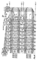
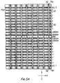
- Athird NAND circuit49 and a fourth NAND circuit 50 are arranged in the same manner as first and second NAND circuits 46, 47.
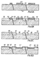
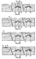
- a protective film 84 such as a BPSG (boron-doped phospho-silicate glass) film or PSG film or silicon nitride film, of 500 to 700 nm (5000 to 7000A) thickness is deposited over the surface by the plasma CVD method.
- the surface protective film 84 is formed with concave regions corresponding to the depletion type transistors which represent the stored information. Accordingly, it is possible to check the stored information from the outer configuration of the device.
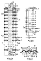
- a bonding pad 81 for an outer-lead is exposed, and the chip fabricating process is completed.
- an outer-lead 86 made from aluminium is connected to the bonding pad 81.
Landscapes
- Semiconductor Memories (AREA)
- Read Only Memory (AREA)
Claims (4)
Applications Claiming Priority (2)
| Application Number | Priority Date | Filing Date | Title |
|---|---|---|---|
| JP56128450A JPS5830154A (ja) | 1981-08-17 | 1981-08-17 | 固定記憶半導体装置およびその製造方法 |
| JP128450/81 | 1981-08-17 |
Publications (4)
| Publication Number | Publication Date |
|---|---|
| EP0073130A2 EP0073130A2 (de) | 1983-03-02 |
| EP0073130A3 EP0073130A3 (en) | 1985-01-16 |
| EP0073130B1 EP0073130B1 (de) | 1988-03-02 |
| EP0073130B2 true EP0073130B2 (de) | 1993-05-12 |
Family
ID=14985006
Family Applications (1)
| Application Number | Title | Priority Date | Filing Date |
|---|---|---|---|
| EP82304312A Expired - Lifetime EP0073130B2 (de) | 1981-08-17 | 1982-08-16 | Verfahren zur Herstellung eines Nur-Lesespeichers vom Maskentyp |
Country Status (4)
| Country | Link |
|---|---|
| US (1) | US4467520A (de) |
| EP (1) | EP0073130B2 (de) |
| JP (1) | JPS5830154A (de) |
| DE (1) | DE3278182D1 (de) |
Families Citing this family (29)
| Publication number | Priority date | Publication date | Assignee | Title |
|---|---|---|---|---|
| US4536944A (en) * | 1982-12-29 | 1985-08-27 | International Business Machines Corporation | Method of making ROM/PLA semiconductor device by late stage personalization |
| US4513494A (en) * | 1983-07-19 | 1985-04-30 | American Microsystems, Incorporated | Late mask process for programming read only memories |
| JPS60174682A (ja) * | 1984-02-20 | 1985-09-07 | Tsukahara Kogyo Kk | 弾力性を有する多孔性印材の製造方法 |
| JPS61287164A (ja) * | 1985-06-13 | 1986-12-17 | Ricoh Co Ltd | 半導体メモリ装置 |
| JPH06104358B2 (ja) * | 1985-06-24 | 1994-12-21 | 塚原工業株式会社 | インキ吸蔵型印判材の製造方法 |
| JPS6292362A (ja) * | 1985-10-17 | 1987-04-27 | Toshiba Corp | 半導体装置の製造方法 |
| JP2723147B2 (ja) * | 1986-06-25 | 1998-03-09 | 株式会社日立製作所 | 半導体集積回路装置の製造方法 |
| JPS6381948A (ja) * | 1986-09-26 | 1988-04-12 | Toshiba Corp | 多層配線半導体装置 |
| US5068696A (en) * | 1989-03-31 | 1991-11-26 | Texas Instruments Incorporated | Programmable interconnect or cell using silicided MOS transistors |
| US5019878A (en) * | 1989-03-31 | 1991-05-28 | Texas Instruments Incorporated | Programmable interconnect or cell using silicided MOS transistors |
| US5091328A (en) * | 1989-11-21 | 1992-02-25 | National Semiconductor Corporation | Method of late programming MOS devices |
| IT1239989B (it) * | 1990-03-30 | 1993-11-27 | Sgs Thomson Microelectronics | Struttura di cella programmata,a bassa capacita' e ad elevata tensione di rottura, per circuiti di memoria a sola lettura |
| US5486487A (en) * | 1990-03-30 | 1996-01-23 | Sgs-Thomson Microelectronics S.R.L. | Method for adjusting the threshold of a read-only memory to achieve low capacitance and high breakdown voltage |
| JPH0487370A (ja) * | 1990-07-30 | 1992-03-19 | Sharp Corp | 半導体装置の製造方法 |
| US5200355A (en) * | 1990-12-10 | 1993-04-06 | Samsung Electronics Co., Ltd. | Method for manufacturing a mask read only memory device |
| JP2604071B2 (ja) * | 1991-05-14 | 1997-04-23 | 株式会社東芝 | 半導体装置の製造方法 |
| US5432103A (en) * | 1992-06-22 | 1995-07-11 | National Semiconductor Corporation | Method of making semiconductor ROM cell programmed using source mask |
| KR0140691B1 (ko) * | 1992-08-20 | 1998-06-01 | 문정환 | 반도체 장치의 마스크롬 제조방법 |
| JP3177036B2 (ja) * | 1992-12-24 | 2001-06-18 | 三菱鉛筆株式会社 | 連続気泡を有するスポンジゴム印字体の製造方法 |
| US5592012A (en) * | 1993-04-06 | 1997-01-07 | Sharp Kabushiki Kaisha | Multivalued semiconductor read only storage device and method of driving the device and method of manufacturing the device |
| US5429974A (en) * | 1993-10-22 | 1995-07-04 | United Microelectronics Corporation | Post passivation mask ROM programming method |
| US5514609A (en) * | 1994-05-13 | 1996-05-07 | Mosel Vitelic, Inc. | Through glass ROM code implant to reduce product delivering time |
| US5796149A (en) * | 1994-09-09 | 1998-08-18 | Nippon Steel Corporation | Semiconductor memory using different concentration impurity diffused layers |
| US5514610A (en) * | 1995-03-17 | 1996-05-07 | Taiwan Semiconductor Manufacturing Company | Method of making an optimized code ion implantation procedure for read only memory devices |
| GB2300983A (en) * | 1995-05-13 | 1996-11-20 | Holtek Microelectronics Inc | Flexible CMOS IC layout method |
| US5693551A (en) * | 1995-09-19 | 1997-12-02 | United Microelectronics, Corporation | Method for fabricating a tri-state read-only memory device |
| IT1288720B1 (it) * | 1996-10-01 | 1998-09-24 | Skf Ind Spa | Mozzo o gruppo mozzo ruota che permette un migliore montaggio e smontaggio di un organo frenante. |
| IT1289781B1 (it) * | 1996-12-20 | 1998-10-16 | Skf Ind Spa | Unita' mozzo-ruota, in particolare per un autoveicolo. |
| US6238983B1 (en) * | 1999-08-30 | 2001-05-29 | Taiwan Semiconductor Manufacturing Company | Alignment dip back oxide and code implant through poly to approach the depletion mode device character |
Family Cites Families (14)
| Publication number | Priority date | Publication date | Assignee | Title |
|---|---|---|---|---|
| US3914855A (en) * | 1974-05-09 | 1975-10-28 | Bell Telephone Labor Inc | Methods for making MOS read-only memories |
| JPS5851427B2 (ja) * | 1975-09-04 | 1983-11-16 | 株式会社日立製作所 | 絶縁ゲ−ト型リ−ド・オンリ−・メモリの製造方法 |
| JPS5333076A (en) * | 1976-09-09 | 1978-03-28 | Toshiba Corp | Production of mos type integrated circuit |
| JPS5375781U (de) * | 1976-11-29 | 1978-06-24 | ||
| US4108686A (en) * | 1977-07-22 | 1978-08-22 | Rca Corp. | Method of making an insulated gate field effect transistor by implanted double counterdoping |
| US4384399A (en) * | 1978-03-20 | 1983-05-24 | Texas Instruments Incorporated | Method of making a metal programmable MOS read only memory device |
| DE2909197A1 (de) * | 1978-03-20 | 1979-10-04 | Texas Instruments Inc | Verfahren zur herstellung eines festspeichers und festspeichermatrix |
| US4364167A (en) * | 1979-11-28 | 1982-12-21 | General Motors Corporation | Programming an IGFET read-only-memory |
| US4336647A (en) * | 1979-12-21 | 1982-06-29 | Texas Instruments Incorporated | Method of making implant programmable N-channel read only memory |
| US4356042A (en) * | 1980-11-07 | 1982-10-26 | Mostek Corporation | Method for fabricating a semiconductor read only memory |
| US4406049A (en) * | 1980-12-11 | 1983-09-27 | Rockwell International Corporation | Very high density cells comprising a ROM and method of manufacturing same |
| US4380866A (en) * | 1981-05-04 | 1983-04-26 | Motorola, Inc. | Method of programming ROM by offset masking of selected gates |
| US4365405A (en) * | 1981-05-28 | 1982-12-28 | General Motors Corporation | Method of late programming read only memory devices |
| US4364165A (en) * | 1981-05-28 | 1982-12-21 | General Motors Corporation | Late programming using a silicon nitride interlayer |
-
1981
- 1981-08-17 JP JP56128450A patent/JPS5830154A/ja active Granted
-
1982
- 1982-08-16 EP EP82304312A patent/EP0073130B2/de not_active Expired - Lifetime
- 1982-08-16 DE DE8282304312T patent/DE3278182D1/de not_active Expired
- 1982-08-17 US US06/408,873 patent/US4467520A/en not_active Expired - Lifetime
Also Published As
| Publication number | Publication date |
|---|---|
| EP0073130A3 (en) | 1985-01-16 |
| JPH0328832B2 (de) | 1991-04-22 |
| EP0073130A2 (de) | 1983-03-02 |
| JPS5830154A (ja) | 1983-02-22 |
| US4467520A (en) | 1984-08-28 |
| DE3278182D1 (en) | 1988-04-07 |
| EP0073130B1 (de) | 1988-03-02 |
Similar Documents
| Publication | Publication Date | Title |
|---|---|---|
| EP0073130B2 (de) | Verfahren zur Herstellung eines Nur-Lesespeichers vom Maskentyp | |
| US6312990B1 (en) | Structure nonvolatile semiconductor memory cell array and method for fabricating same | |
| US4080718A (en) | Method of modifying electrical characteristics of MOS devices using ion implantation | |
| US4766088A (en) | Method of making a memory device with polysilicon electrodes | |
| US4755864A (en) | Semiconductor read only memory device with selectively present mask layer | |
| US5063170A (en) | Semiconductor integrated circuit device and a method of producing the same | |
| US5517061A (en) | CMOS read only memory with programming at the second metal layer on a two-metal process | |
| JP2509706B2 (ja) | マスクromの製造方法 | |
| US4219836A (en) | Contact programmable double level polysilicon MOS read only memory | |
| US4151020A (en) | High density N-channel silicon gate read only memory | |
| US5149667A (en) | Mask ROM device having double polycrystalline silicone and process for producing the same | |
| US4385432A (en) | Closely-spaced double level conductors for MOS read only | |
| US4326329A (en) | Method of making a contact programmable double level polysilicon MOS read only memory | |
| US4271421A (en) | High density N-channel silicon gate read only memory | |
| US4342100A (en) | Implant programmable metal gate MOS read only memory | |
| KR100251229B1 (ko) | 노아형 마스크 롬의 개선된 구조 및 그 제조방법 | |
| US6150198A (en) | Method of fabricating semiconductor read-only memory device with reduced parastic capacitance between bit line and word line | |
| US6353243B1 (en) | Process for manufacturing an integrated circuit comprising an array of memory cells | |
| US4336647A (en) | Method of making implant programmable N-channel read only memory | |
| EP0447976A1 (de) | Nur-Lese-Halbleiterspeicheranordnung | |
| US5949704A (en) | Stacked read-only memory | |
| US7157336B2 (en) | Method of manufacturing semiconductor device | |
| JP2834179B2 (ja) | 半導体集積回路装置の製造方法 | |
| EP0925609B1 (de) | Gestapelte nur-lese-speicheranordnung | |
| JPH08321561A (ja) | 半導体メモリ装置とその製造方法 |
Legal Events
| Date | Code | Title | Description |
|---|---|---|---|
| PUAI | Public reference made under article 153(3) epc to a published international application that has entered the european phase |
Free format text: ORIGINAL CODE: 0009012 |
|
| AK | Designated contracting states |
Designated state(s): DE FR GB |
|
| RAP1 | Party data changed (applicant data changed or rights of an application transferred) |
Owner name: KABUSHIKI KAISHA TOSHIBA |
|
| PUAL | Search report despatched |
Free format text: ORIGINAL CODE: 0009013 |
|
| RHK1 | Main classification (correction) |
Ipc: H01L 29/82 |
|
| AK | Designated contracting states |
Designated state(s): DE FR GB |
|
| 17P | Request for examination filed |
Effective date: 19850621 |
|
| 17Q | First examination report despatched |
Effective date: 19860404 |
|
| GRAA | (expected) grant |
Free format text: ORIGINAL CODE: 0009210 |
|
| AK | Designated contracting states |
Kind code of ref document: B1 Designated state(s): DE FR GB |
|
| REF | Corresponds to: |
Ref document number: 3278182 Country of ref document: DE Date of ref document: 19880407 |
|
| ET | Fr: translation filed | ||
| PLBI | Opposition filed |
Free format text: ORIGINAL CODE: 0009260 |
|
| 26 | Opposition filed |
Opponent name: DEUTSCHE ITT INDUSTRIES GMBH, FREIBURG Effective date: 19881201 |
|
| ET1 | Fr: translation filed ** revision of the translation of the patent or the claims | ||
| PUAH | Patent maintained in amended form |
Free format text: ORIGINAL CODE: 0009272 |
|
| STAA | Information on the status of an ep patent application or granted ep patent |
Free format text: STATUS: PATENT MAINTAINED AS AMENDED |
|
| 27A | Patent maintained in amended form |
Effective date: 19930512 |
|
| AK | Designated contracting states |
Kind code of ref document: B2 Designated state(s): DE FR GB |
|
| ET | Fr: translation filed |
Free format text: BO 12/93 PAGE 167: ANNULATION |
|
| ET3 | Fr: translation filed ** decision concerning opposition | ||
| PGFP | Annual fee paid to national office [announced via postgrant information from national office to epo] |
Ref country code: GB Payment date: 19970807 Year of fee payment: 16 |
|
| PGFP | Annual fee paid to national office [announced via postgrant information from national office to epo] |
Ref country code: FR Payment date: 19970811 Year of fee payment: 16 |
|
| PGFP | Annual fee paid to national office [announced via postgrant information from national office to epo] |
Ref country code: DE Payment date: 19970822 Year of fee payment: 16 |
|
| PG25 | Lapsed in a contracting state [announced via postgrant information from national office to epo] |
Ref country code: GB Free format text: LAPSE BECAUSE OF NON-PAYMENT OF DUE FEES Effective date: 19980816 |
|
| GBPC | Gb: european patent ceased through non-payment of renewal fee |
Effective date: 19980816 |
|
| PG25 | Lapsed in a contracting state [announced via postgrant information from national office to epo] |
Ref country code: FR Free format text: LAPSE BECAUSE OF NON-PAYMENT OF DUE FEES Effective date: 19990430 |
|
| PG25 | Lapsed in a contracting state [announced via postgrant information from national office to epo] |
Ref country code: DE Free format text: LAPSE BECAUSE OF NON-PAYMENT OF DUE FEES Effective date: 19990601 |
|
| REG | Reference to a national code |
Ref country code: FR Ref legal event code: ST |
|
| APAH | Appeal reference modified |
Free format text: ORIGINAL CODE: EPIDOSCREFNO |