EP0059465B1 - Pulse modulator - Google Patents
Pulse modulator Download PDFInfo
- Publication number
- EP0059465B1 EP0059465B1 EP82101549A EP82101549A EP0059465B1 EP 0059465 B1 EP0059465 B1 EP 0059465B1 EP 82101549 A EP82101549 A EP 82101549A EP 82101549 A EP82101549 A EP 82101549A EP 0059465 B1 EP0059465 B1 EP 0059465B1
- Authority
- EP
- European Patent Office
- Prior art keywords
- pulse
- pulse modulator
- input
- input quantity
- output
- Prior art date
- Legal status (The legal status is an assumption and is not a legal conclusion. Google has not performed a legal analysis and makes no representation as to the accuracy of the status listed.)
- Expired
Links
Images

Classifications
-
- H—ELECTRICITY
- H03—ELECTRONIC CIRCUITRY
- H03K—PULSE TECHNIQUE
- H03K7/00—Modulating pulses with a continuously-variable modulating signal
- H03K7/06—Frequency or rate modulation, i.e. PFM or PRM
Definitions
- the invention relates in general to an improved pulse modulator for converting analog information into a series of pulses.
- PPM pulse period modulation
- a pulse modulator for providing pulses having a predetermined parameter proportional to at least one input quantity, comprising a circuit already known from "Electronic Design", volume 19, number 5, March 4, 1971, page 58; Ronald R. Siebert: "Precision ramp generator responds to clock in 25ns".
- the known circuit comprises energy storage means (capacitor C) being charged by a first input quantity to provide a changing quantity (I CHARGE), a first comparator (CA) comparing a second input quantity (Y R1) with said changing quantity, said first comparator (CA) providing a predetermined signal when the compared quantities have a predetermined relationship, means including a second comparator (CB) comparing said changing quantity (I CHARGE) with a reference value (NR2), the predetermined signal being provided by said first comparator (CA) for providing a first discharge signal, a switch (S2) connected across the energy storage means (C) for enabling said energy storage means (C) to be charged by said first input quantity (I CHARGE), an R-S flip-flop having set and reset inputs, with the outputs of the first and second comparators being connected to the set and reset inputs, respectively, of said R-S flip-flop, and wherein the second comparator (CB) resets and then enables said R-S flip-flop (FF2) in response to the energy storage
- This circuit in connection with a source for constant current (I CHARGE) forms a ramp generator, not a pulse modulator.
- the input V R1 of CA may be used at the second input for the second input quantity.
- FFa flip-flop
- a monostable multivibrator may be used, as known from "Radio frequencyen Elektronik", Vol. 29, number 4, 1980, pages 257 to 260, Berlin (DDR); H. Kulim: “Spannungs-Frequenz-wandler", see page 257, second column, line 4, to the right hand column, third paragraph and page 258, middle column, last paragraph.
- the chief object of the present invention is to provide a versatile pulse modulator which offers application flexibility merely by the selection of certain modes for its input signals, while obviating the start-up and latch-up problems of the past and which may be easily-manufactured at relatively low cost.
- an improved pulse modulator is to be constructed which forces the desired oscillatory mode, regardless of how electrical power is initially applied thereto. It should not require either a predetermined edge or level change in the power supply, in order to properly start operation. Circuit oscillation should be achieved by charging energy storage means, such as a capacitor, and by discharging the capacitor each time a predetermined relationship occurs between first and second input quantities.
- the monitoring means should provide an auxiliary discharge signal for discharging the capacitor when the predetermined relationship between the input quantities occurs, but the capacitor should not be discharged in response thereto.
- the pulse modulator should provide application flexibility. By maintaining the first input quantity constant, the modulator should provide linear pulse period modulation in response to the magnitude of the second input quantity. By maintaining the second input quantity constant, the modulator should provide linear pulse frequency modulation (PFM) in response to the magnitude of the first input quantity. When both input quantities are time varying, the modulator should provide a pulse period which is an analog division of the two input quantities.
- PFM pulse frequency modulation
- the said R-S flip-flop consists of two cross coupled NAND gates.
- the said means for providing the second discharge signal is either a monostable multivibrator or a one-shot circuit.
- the present invention reveals an inproved pulse modulator which forces the desired oscillatory mode, regardless of how electrical power is initially applied thereto. It does not require either a predetermined edge or level change in the power supply, in order to properly start operation. Circuit oscillation is achieved by charging energy storage means, such as a capacitor, and by discharging the capacitor each time a predetermined relationship occurs between first and second input quantities. Latch-up or failure to oscillate due to failure to discharge the capacitor when the predetermined relationship occurs is prevented by monitoring means. The monitoring means provides an auxiliary discharge signal for discharging the capacitor when the predetermined relationship between the input quantities occurs, but the capacitor is not discharged in response thereto.
- energy storage means such as a capacitor
- the pulse modulator provides application flexibility. By maintaining the first input quantity constant, the modulator provides linear pulse period modulation in response to the magnitude of the second input quantity. By maintaining the second input quantity constant, the modulator provides linear pulse frequency modulation (PFM) in response to the magnitude of the first input quantity. When both input quantities are time varying, the modulator provides a pulse period which is an analog division of the two input quantities.
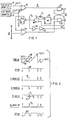
- Pulse modulator 10 includes a source 12 for providing a first input quantity, and a source 14 for providing a second input quantity.
- the first input quantity 12 is connected to charge energy storage means, such as a capacitor 16, to provide a changing quantity at terminal 18.
- the changing quantity at terminal 18 is compared with the second input quantity 14 via a first comparator 20.
- the output of comparator 20 goes low to set an R-S flip-flop 22.
- Flip-flop 22 which may be constructed of cross-coupled NAND gates 24 and 26, is initially in its reset state via the first comparator 20, which is connected to an input of NAND gate 24, and via a second comparator 28.
- the second comparator 28 compares the changing quantity, i.e., the charge voltage on capacitor 16, with a predetermined small voltage determined by a voltage divider 30.
- the output of comparator 20 is high, i,e., a logic one
- the output of comparator 28 is low, i.e., a logic zero. This relationship resets flip-flop 22 such that NAND gate 24 outputs a logic zero and NAND gate 26 outputs a logic one.
- a monostable multivibrator (MV) or 1-shot 32 is connected to be triggered by NAND gate 24 when flip-flop 22 is toggled, such as by the positive going edge of the output of NAND gate 24.
- the Q output of MV 32 goes low for a very short period of time To, with the Q output being applied to one input of a dual input NAND gate 34.
- the output of NAND gate 34 is applied to the control input of an analog switch 36.
- Analog switch 36 has its input and output terminals connected across capacitor 16.
- the pulse output of modulator 10 may be taken from any convenient circuit location, including the output of comparator 20, the output of one of the NAND gates of flip-flop 22, the Q or Q of MV 32, or the output of NAND gate 34.
- the output of NAND gate 34 has been chosen, with inverter gates 40 and 42 applying the output pulse P o to an output terminal 44.
- flip-flop 22 and the second comparator 28 cooperatively monitor the operation of the circuit to prevent circuit latch-up during operation, should MV 32 for some reason fail to be triggered when flip-flop 22 is toggled.
- the output of comparator 28 goes from low to high shortly after capacitor 16 starts charging.
- NAND gate 24 goes high, if MV 32 fails to timely provide a pulse which results in the discharge of capacitor 16, NAND gate 26 will have two high inputs and its output Q will be low. This output is tied to the other input of NAND gate 34.
- the selection of the ouput of NAND gate 34 for providing the output pulses from pulse modulator 10 thus assures that there will be no missing pulses in the output train of pulses, which might occur had the Q, or Q, output of MV 32 been selected to provide the output pulses.
- the pulse period T(t) is given by the relationship: where To is the time width of the output pulse P, of MV 32, and C is the capacitance of capacitor 16. If To is made very small in comparison with the desired range of operation, equation (1) is substantially equal to;
- the output pulse period is responsive to an analog division of Vx(t) by ly(t), as set forth in equation (2), and thus the pulse modulator 10 functions as an analog divider.
- the pulse period T(t) is directly proportional to the magnitude of the second input quantity V,(t), and thus the pulse modulator 10 functions as a linear pulse period modulator (PPM).
- PPM linear pulse period modulator
- Equation (2) may be written: where F(t) is the pulse frequency. If the second input quantity V x (t) is held constant, the pulse modulator 10 will function as a linear frequency modulator.
- the pulse modulator 10 shown in Figure 1 may be modified to supply a nominal period, or a nominal frequency, when ly(t), or V x (t), respectively, is equal to zero, by proper biasing, i.e., by injecting a D.C. component into V x or ly, or both.
- This modification allows V x (t) and ly(t) to be bi-polar.
- FIG 2 is a schematic diagram which illustrates the use of the pulse modulator 10 of Figure 1 which may be used in a transmitter 32 shown for example in Figure 1 of U.S. Patent 4,275,429. The disclosure therein reveals a complete protective relaying function which may advantageously utilize the present invention.
- the first input quantity ly(t) is a constant current source, and thus the pulse modulator functions as a linear pulse period modulator.
- the second input quantity V x (t) is provided by the current derived voltage signal V N which is obtained from the sequence filters which combine the positive, negative and zero sequence currents of the 3- phase electrical transmission system, to provide a single-phase voltage signal V N .
- Signal V N is sent to a remote terminal via PPM on any suitable communication channel, such as an optical fiber link, telephone, power line carrier, or microwave, where it is demodulated and compared with a similarly derived signal V F .
- signal V F is modulated via a similar pulse period modulator and sent to the local terminal where it is demodulated and compared with signal V N .
- the functions of Figure 2 which are the same as those of Figure 1 are given like reference numerals, and the functions which are only slightly modified are given the same reference numerals along with a prime mark.
- signal V N is conditioned in amplifier 50 and applied to the non-inverting input of comparator 20 via resistor 52. Suitable bias is provided via a voltage source V+ which is connected to the non-inverting input via a resistor 57. This permits signal V N to be bi-polar, as hereinbefore explained.
- the first input quantity 12 which comes from a constant current source, is connected to charge capacitor 16, and the charge on capacitor 16 becomes an input of comparator 20.
- the output of comparator 20 is connected to the set input of flip-flop 22 via a resistor 56.
- the second comparator 28 compares the charge on capacitor 16 with a predetermined voltage provided by a voltage divider 30', and the output of comparator 28 is connected to the reset input of flip-flop 22 via a resistor 58.
- the Q output of flip-flop 22 is connected to the trigger input of MV 32, which for purposes of example is illustrated as being one-half of Motorala's Dual Precision Monostable Multivibrator MC14538B.
- the Q output of MV 32 is connected to one input of NAND gate 34, and the output of NAND gate 34 is connected to the control input of analog switch 36, which may be one of the switches in RCA's Quad Bilateral Switch CD4066, for example.
- Figure 3 is a graph which illustrates some of the waveforms developed in the transmitter 38 shown in Figure 2.
- the output of comparator 20 is a logic one and the output of comparator 28 is a logic zero, which resets flip-flop 22 such that the Q and Q outputs are logic zero and logic one, respectively.
- the charge on capacitor 16 starts at zero at point 60 and the charge voltage, which is proportional to ly(t), increases linearly along curve portion 62.
- curve portion 62 reaches the voltage provided by voltage divider 30', the output of comparator 28 switches from logic zero to logic one at point 64, to enable flip-flop 22.
- Capacitor 16 continues to charge and when curve portion 62 reaches a level V x (t) responsive to signal V N at point 66, the output of comparator 20 switches low at point 68.
- Flip-flop 22 is toggled and the positive going edge 70 of its Q output triggers MV 32 to provide a pulse 72, which is the same as pulse P j , having a logic zero time duration of To.
- Logic zero pulse 72 causes NAND gate 34 to provide a logic one pulse P o which closes switch 36 to discharge capacitor 16 along curve portion 74.
- Comparators 20 and 28 then revert to their logic one and logic zero outputs, respectively, to reset flip-flop 22 and enable the cycle to be repeated.
- the frequency range of the pulse modulator circuit is deliberately selected to be high, such as about a 110 KHz center frequency, for example. This relatively high frequency reduces the size of the circuit components, and is also needed for encoding due to capacitance and current source level limitations.
- a divide-by-N counter 90 may be provided to obtain the desired frequency range for the specific communication link to be used, which is hereinbefore stated may be a fiber optic link, a telephone data channel, a microwave link, or a power line carrier link, for example.
- the divide-by-N counter 90 is illustrated as being Motorola's Seven Stage Ripple Counter MC14024B.
- the pulses are inverted via an inverter gate 92 and applied to the clock input of counter 90.
- the appropriate Q output of counter 90 is selected as the output, depending upon the division required, and the output is inverted via gate 94 and applied to the output terminal 44 for transmission over the communication channel.
- the pulse modulator is free of latch-up problems which may be associated with failure of a monostable multivibrator to provide a timely pulse.
- the pulse modulator of the invention is versatile in that it may be used as an analog divider of two time varying inputs, a linear pulse period modulator, or a linear pulse frequency modulator, merely by proper selection of the input signals.
- a divide-by-N counter on the output of the pulse modulator provides interface flexibility for properly matching the selected communication channel.
Landscapes
- Manipulation Of Pulses (AREA)
- Analogue/Digital Conversion (AREA)
- Amplifiers (AREA)
Applications Claiming Priority (2)
| Application Number | Priority Date | Filing Date | Title |
|---|---|---|---|
| US06/239,917 US4380746A (en) | 1981-03-03 | 1981-03-03 | Pulse modulator using capacitor charging and discharging circuits |
| US239917 | 1988-09-02 |
Publications (2)
| Publication Number | Publication Date |
|---|---|
| EP0059465A1 EP0059465A1 (en) | 1982-09-08 |
| EP0059465B1 true EP0059465B1 (en) | 1987-06-24 |
Family
ID=22904302
Family Applications (1)
| Application Number | Title | Priority Date | Filing Date |
|---|---|---|---|
| EP82101549A Expired EP0059465B1 (en) | 1981-03-03 | 1982-03-01 | Pulse modulator |
Country Status (9)
| Country | Link |
|---|---|
| US (1) | US4380746A (enExample) |
| EP (1) | EP0059465B1 (enExample) |
| JP (1) | JPS57157624A (enExample) |
| BR (1) | BR8201039A (enExample) |
| CA (1) | CA1167533A (enExample) |
| DE (1) | DE3276649D1 (enExample) |
| ES (1) | ES510046A0 (enExample) |
| MX (1) | MX151477A (enExample) |
| ZA (1) | ZA821185B (enExample) |
Cited By (1)
| Publication number | Priority date | Publication date | Assignee | Title |
|---|---|---|---|---|
| DE102005044801B4 (de) * | 2005-09-20 | 2013-08-01 | Zinoviy Lerner | Modulator zur Frequenzmodulation von Rechteckschwingungen |
Families Citing this family (21)
| Publication number | Priority date | Publication date | Assignee | Title |
|---|---|---|---|---|
| JPS5819026A (ja) * | 1981-07-24 | 1983-02-03 | Nec Corp | パルス幅変調回路 |
| US4471286A (en) * | 1982-04-09 | 1984-09-11 | Westinghouse Electric Corp. | Closed-loop frequency regulated generator apparatus |
| US4510453A (en) * | 1982-07-13 | 1985-04-09 | Westinghouse Electric Corp. | Frequency modulation or pulse modulation demodulator |
| JPS60136412A (ja) * | 1983-12-26 | 1985-07-19 | Toshiba Corp | 電圧制御型可変周波数パルス発振器 |
| US4813057A (en) * | 1984-12-03 | 1989-03-14 | Charles A. Phillips | Time domain radio transmission system |
| USRE39759E1 (en) | 1984-12-03 | 2007-08-07 | Time Domain Corporation | Time domain radio transmission system |
| US6606051B1 (en) | 1984-12-03 | 2003-08-12 | Time Domain Corporation | Pulse-responsive dipole antenna |
| US4641317A (en) * | 1984-12-03 | 1987-02-03 | Charles A. Phillips | Spread spectrum radio transmission system |
| US20030016157A1 (en) * | 1984-12-03 | 2003-01-23 | Fullerton Larry W. | Time domain radio transmission system |
| USRE41479E1 (en) | 1984-12-03 | 2010-08-10 | Time Domain Corporation | Time domain radio transmission system |
| US6882301B2 (en) | 1986-06-03 | 2005-04-19 | Time Domain Corporation | Time domain radio transmission system |
| US4908526A (en) * | 1988-06-03 | 1990-03-13 | Harris Corporation | Pulse generator output voltage calibration circuit |
| US4935837A (en) * | 1989-04-03 | 1990-06-19 | Abb Power T&D Company Inc. | Phase comparison relaying system with single channel communications link |
| JPH0496105U (enExample) * | 1991-01-18 | 1992-08-20 | ||
| DE69203386T2 (de) * | 1991-05-17 | 1996-03-07 | Gallagher Electronics Ltd | Übertragungsverfahren und -vorrichtung. |
| US5592111A (en) * | 1994-12-14 | 1997-01-07 | Intel Corporation | Clock speed limiter for an integrated circuit |
| SE511963C2 (sv) * | 1997-04-23 | 1999-12-20 | Ericsson Telefon Ab L M | Anordning och förfarande för bestämning av linjespänning i en abonnentlinjekrets |
| GB2337649B (en) * | 1998-05-23 | 2000-06-07 | Plessey Telecomm | Voltage-controlled oscillator |
| US7466178B2 (en) * | 2005-02-15 | 2008-12-16 | Fred Mirow | Multivibrator with reduced average offset voltage |
| JP2007128380A (ja) * | 2005-11-07 | 2007-05-24 | Nec Electronics Corp | 電源ic |
| US10601408B2 (en) * | 2018-04-13 | 2020-03-24 | Texas Instruments Incorporated | Low frequency oscillator with ultra-low short circuit current |
Family Cites Families (5)
| Publication number | Priority date | Publication date | Assignee | Title |
|---|---|---|---|---|
| US3639779A (en) * | 1971-03-15 | 1972-02-01 | Gte Sylvania Inc | Limiter circuit with enable function |
| US3742384A (en) * | 1971-06-07 | 1973-06-26 | Texas Instruments Inc | Variable frequency oscillator |
| JPS5843922B2 (ja) * | 1975-02-24 | 1983-09-30 | ソニー株式会社 | パルスハバヘンチヨウゾウフクカイロ |
| US4187439A (en) * | 1976-12-07 | 1980-02-05 | The Cessna Aircraft Company | Analog control of pulse rates |
| GB1585936A (en) * | 1978-04-26 | 1981-03-11 | Philips Electronic Associated | Phase modulator circuit |
-
1981
- 1981-03-03 US US06/239,917 patent/US4380746A/en not_active Expired - Lifetime
-
1982
- 1982-02-22 CA CA000396754A patent/CA1167533A/en not_active Expired
- 1982-02-23 ZA ZA821185A patent/ZA821185B/xx unknown
- 1982-03-01 JP JP57030676A patent/JPS57157624A/ja active Granted
- 1982-03-01 DE DE8282101549T patent/DE3276649D1/de not_active Expired
- 1982-03-01 BR BR8201039A patent/BR8201039A/pt not_active IP Right Cessation
- 1982-03-01 EP EP82101549A patent/EP0059465B1/en not_active Expired
- 1982-03-01 MX MX191626A patent/MX151477A/es unknown
- 1982-03-02 ES ES510046A patent/ES510046A0/es active Granted
Non-Patent Citations (1)
| Title |
|---|
| ELECTRONIC DESIGN, vol. 19, no. 5, 4th March 1971, page 58; SIEBERT: "Precision ramp generator responds to clock in 25 ns" * |
Cited By (1)
| Publication number | Priority date | Publication date | Assignee | Title |
|---|---|---|---|---|
| DE102005044801B4 (de) * | 2005-09-20 | 2013-08-01 | Zinoviy Lerner | Modulator zur Frequenzmodulation von Rechteckschwingungen |
Also Published As
| Publication number | Publication date |
|---|---|
| BR8201039A (pt) | 1983-01-04 |
| ZA821185B (en) | 1983-03-30 |
| ES8305541A1 (es) | 1983-04-01 |
| DE3276649D1 (en) | 1987-07-30 |
| JPS57157624A (en) | 1982-09-29 |
| CA1167533A (en) | 1984-05-15 |
| JPH0245852B2 (enExample) | 1990-10-12 |
| EP0059465A1 (en) | 1982-09-08 |
| US4380746A (en) | 1983-04-19 |
| ES510046A0 (es) | 1983-04-01 |
| MX151477A (es) | 1984-11-29 |
Similar Documents
| Publication | Publication Date | Title |
|---|---|---|
| EP0059465B1 (en) | Pulse modulator | |
| EP0492538B1 (en) | Interface circuit including DC/DC converter | |
| EP0129181A3 (en) | Dc-dc converter | |
| GB1387207A (en) | Repeater power-supply system | |
| US4660002A (en) | High frequency oscillator using a diode for frequency switching and FM modulation | |
| GB1536623A (en) | Integrated circuits | |
| US3506848A (en) | Pulse width to analog signal converter | |
| GB1532677A (en) | Voltage dropping circuit | |
| JPS57202124A (en) | Digital-to-analog converting circuit | |
| SU474816A1 (ru) | Релейный операционный усилитель | |
| SU1059654A1 (ru) | Трехканальный резервированный генератор | |
| SU824389A1 (ru) | Инвертор | |
| SU902167A1 (ru) | Стабилизированный транзисторный конвертор | |
| KR910005742B1 (ko) | 바테리의 급속충전 제어방식 | |
| KR880001799B1 (ko) | 영상 신호 전송용 펄스 주파수 변조장치 | |
| KR890004973Y1 (ko) | 상태변화 감지회로 | |
| JPH0234543B2 (ja) | Reberuhenkankairo | |
| SU1030962A1 (ru) | Генератор пилообразного тока | |
| EP0158210A3 (en) | Ratio discriminator | |
| SU1418868A1 (ru) | Преобразователь посто нного напр жени в посто нное | |
| SU1088632A1 (ru) | Генератор импульсов напр жени | |
| CA1216639A (en) | Voltage controlled pulse width modulation circuit | |
| SU1347156A1 (ru) | Импульсный модул тор | |
| WO1987007991A1 (en) | Local oscillation apparatus | |
| SU1265916A1 (ru) | Устройство дл зар да аккумул торной батареи |
Legal Events
| Date | Code | Title | Description |
|---|---|---|---|
| PUAI | Public reference made under article 153(3) epc to a published international application that has entered the european phase |
Free format text: ORIGINAL CODE: 0009012 |
|
| AK | Designated contracting states |
Designated state(s): DE FR GB IT SE |
|
| 17P | Request for examination filed |
Effective date: 19830224 |
|
| GRAA | (expected) grant |
Free format text: ORIGINAL CODE: 0009210 |
|
| AK | Designated contracting states |
Kind code of ref document: B1 Designated state(s): DE FR GB IT SE |
|
| REF | Corresponds to: |
Ref document number: 3276649 Country of ref document: DE Date of ref document: 19870730 |
|
| ET | Fr: translation filed | ||
| ITF | It: translation for a ep patent filed | ||
| PLBE | No opposition filed within time limit |
Free format text: ORIGINAL CODE: 0009261 |
|
| STAA | Information on the status of an ep patent application or granted ep patent |
Free format text: STATUS: NO OPPOSITION FILED WITHIN TIME LIMIT |
|
| 26N | No opposition filed | ||
| PGFP | Annual fee paid to national office [announced via postgrant information from national office to epo] |
Ref country code: SE Payment date: 19900105 Year of fee payment: 9 |
|
| ITTA | It: last paid annual fee | ||
| PG25 | Lapsed in a contracting state [announced via postgrant information from national office to epo] |
Ref country code: SE Effective date: 19910302 |
|
| PGFP | Annual fee paid to national office [announced via postgrant information from national office to epo] |
Ref country code: FR Payment date: 19941215 Year of fee payment: 14 |
|
| PGFP | Annual fee paid to national office [announced via postgrant information from national office to epo] |
Ref country code: GB Payment date: 19941230 Year of fee payment: 14 |
|
| PGFP | Annual fee paid to national office [announced via postgrant information from national office to epo] |
Ref country code: DE Payment date: 19941231 Year of fee payment: 14 |
|
| EUG | Se: european patent has lapsed |
Ref document number: 82101549.2 Effective date: 19911009 |
|
| PG25 | Lapsed in a contracting state [announced via postgrant information from national office to epo] |
Ref country code: GB Effective date: 19960301 |
|
| GBPC | Gb: european patent ceased through non-payment of renewal fee |
Effective date: 19960301 |
|
| PG25 | Lapsed in a contracting state [announced via postgrant information from national office to epo] |
Ref country code: FR Effective date: 19961129 |
|
| PG25 | Lapsed in a contracting state [announced via postgrant information from national office to epo] |
Ref country code: DE Effective date: 19961203 |
|
| REG | Reference to a national code |
Ref country code: FR Ref legal event code: ST |