EP0056972B1 - Procédé et installation pour la fabrication des éléments semiconducteurs selon des paramètres physiques déterminés - Google Patents
Procédé et installation pour la fabrication des éléments semiconducteurs selon des paramètres physiques déterminés Download PDFInfo
- Publication number
- EP0056972B1 EP0056972B1 EP82100337A EP82100337A EP0056972B1 EP 0056972 B1 EP0056972 B1 EP 0056972B1 EP 82100337 A EP82100337 A EP 82100337A EP 82100337 A EP82100337 A EP 82100337A EP 0056972 B1 EP0056972 B1 EP 0056972B1
- Authority
- EP
- European Patent Office
- Prior art keywords
- semiconductor element
- influence
- fact
- radiation
- resistance
- Prior art date
- Legal status (The legal status is an assumption and is not a legal conclusion. Google has not performed a legal analysis and makes no representation as to the accuracy of the status listed.)
- Expired
Links
Images
Classifications
-
- G—PHYSICS
- G01—MEASURING; TESTING
- G01R—MEASURING ELECTRIC VARIABLES; MEASURING MAGNETIC VARIABLES
- G01R31/00—Arrangements for testing electric properties; Arrangements for locating electric faults; Arrangements for electrical testing characterised by what is being tested not provided for elsewhere
- G01R31/28—Testing of electronic circuits, e.g. by signal tracer
- G01R31/302—Contactless testing
- G01R31/308—Contactless testing using non-ionising electromagnetic radiation, e.g. optical radiation
-
- H10P34/42—
Definitions
- the invention relates to a method and a device for producing semiconductor components, in which the doped semiconductor component is irradiated with an optical radiation that changes its properties, the resistance occurring between two measuring tips acting on the semiconductor component is measured within the semiconductor component, and the measurement result for controlling the radiation intensity and duration is used.
- the layer resisted and other physical properties such as. B. the temperature and piezoresistive coefficient, in semiconductors in general, but especially in polycrystalline layers of semiconductors change when these with intense optical radiation, for. B. laser radiation, are treated.
- the physical reason for this is that under the influence of such radiation, the structure in a polycrystalline layer changes, ie the crystal grains increase, the density of the electrical impurities associated with grain sizes and other lattice defects and parameters such as the electrical charge carrier density and the charge carrier lifetime, as well as mobility. All of these structural changes, as well as other phenomena not mentioned here, lead to a change in the above-mentioned physical properties of the components.
- the invention is accordingly based on the object of designing the method of the type mentioned at the outset and a corresponding device in such a way that a high quantitative setting accuracy of a physical property, which can be defined by the functional relationship between the resistance and an influencing variable influencing it, and thus a can achieve consistently high quality of the semiconductor components produced.
- predetermined values of the relevant influencing variable is used, two different fixed values of the influencing variable are set and the two associated resistance values are measured, and that the semiconductor component is repeatedly irradiated with a corresponding intensity of the optical radiation until the component has the two fixed values Influencing variable have set associated resistance values whose difference has a predetermined value.
- the device according to the invention comprises a first radiation source for the optical radiation, an adjusting device for the radiation intensity, an optical adjusting device for the radiation supplied to the semiconductor component and measuring tips acting on the semiconductor component, which are connected to an electrical control for the adjusting device for the radiation intensity, whereby after
- a device for setting predetermined values of an influencing variable is arranged in the region of the component, which influences the resistance occurring between the measuring tips within the semiconductor component.
- the device is designed in such a way that the component can be set to a specific temperature, light irradiation or elastic pretension.
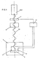
- the method is initially to be explained generally with reference to FIG.
- the sheet resistance of component B is changed by exposing it to intensive radiation S1 directed thereon.
- the radiation which can be laser radiation, is emitted by the radiation source SQ1, e.g. B. generates a laser cannon.
- the radiation S1 passes through a device I for adjusting the intensity of the beam.
- an optical setting device 0 for generating a predetermined pattern is arranged within the beam path.
- Measuring tips M, M 'acting on a test figure of the component record the change and feed it to a control device E1, via which the intensity of the beam S1 can be adjusted.
- the component B is embedded together with the measuring tips M, M 'in a device V in which predetermined values can be used to set the influencing variable influencing the resistance in the semiconductor component.
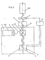
- the device V shown schematically in FIG. 2 can be used to control the change in the temperature of the component B.
- a second radiation source SQ2 is preceded by a time switch Z, which can control the duration of the radiation S2.
- the radiation S2 is directed onto the component B via a mirror system SP, wherein the radiation S1 and S2 can overlap.
- the arrangement is designed in such a way that the radiations S1, S2 or S1 + S2 can optionally be supplied to the component B.
- a temperature increase to T1 is examined there, starting from an initial temperature TO.
- the values R To and R T of the resistance measured at the semiconductor component B 4 correspond to these temperatures.
- a control signal for the intensity of the radiation source S01 is derived from the difference R TO -R T1 , ie the semiconductor component is irradiated with a corresponding intensity of SQ1 until a predetermined value of R TO -R T1 has been set on the component .
- Same temperatures TO and T1 for repeated exposure to radiation source SQ1 are achieved by controlled heating with SQ2 and targeted cooling, e.g. B. reached with a (not shown in det drawing) compressed air jet.
- a precise setting to the temperature coefficient zero is also possible in this way.
- FIG. 2 is only a preferred embodiment. So in addition to the laser heating of B shown, a variety of other techniques, such. B. heating by means of a cross flow through B, heating by external resistance heating, etc., possible and suitable.
- FIG. 2 is also suitable in terms of its structure for adjusting the photosensitivity of components.
- a resistance R L is accordingly obtained for the component under light irradiation, relative to a resistance R o without light irradiation.
- the difference R L - R o can be used to set a predetermined light sensitivity.
- the component For the targeted setting of the piezoresistive coefficient, the component must be placed in two states in which it is biased differently elastically.
- the corresponding resistors are then R d1 and Rd2.
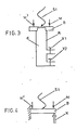
- FIG. 3 shows an embodiment for the device V, the remaining elements, which have been explained in detail with reference to FIG. 1, being omitted for the sake of simplicity.
- the component B here forms the end wall of a container, such as a pipe R.
- a container such as a pipe R.
- the component B can also be firmly clamped on one side, while a mechanical force K, which causes an elastic bending of the component, is allowed to act on the opposite free end.
- the setting is made according to the above description.
Landscapes
- Engineering & Computer Science (AREA)
- Physics & Mathematics (AREA)
- General Engineering & Computer Science (AREA)
- Computer Vision & Pattern Recognition (AREA)
- Electromagnetism (AREA)
- Toxicology (AREA)
- Health & Medical Sciences (AREA)
- General Physics & Mathematics (AREA)
- Photometry And Measurement Of Optical Pulse Characteristics (AREA)
- Cosmetics (AREA)
- Medicines Containing Plant Substances (AREA)
- Organic Low-Molecular-Weight Compounds And Preparation Thereof (AREA)
- Feedback Control In General (AREA)
- Semiconductor Lasers (AREA)
- Testing Or Measuring Of Semiconductors Or The Like (AREA)
Claims (10)
Priority Applications (1)
| Application Number | Priority Date | Filing Date | Title |
|---|---|---|---|
| AT82100337T ATE29339T1 (de) | 1981-01-24 | 1982-01-19 | Verfahren und vorrichtung zur herstellung von halbleiterelementen mit bestimmten physikalischen parametern. |
Applications Claiming Priority (2)
| Application Number | Priority Date | Filing Date | Title |
|---|---|---|---|
| DE3102337 | 1981-01-24 | ||
| DE19813102337 DE3102337A1 (de) | 1981-01-24 | 1981-01-24 | Verfahren und vorrichtung zur herstellung von halbleiterelementen mit bestimmten physikalischen parametern |
Publications (2)
| Publication Number | Publication Date |
|---|---|
| EP0056972A1 EP0056972A1 (fr) | 1982-08-04 |
| EP0056972B1 true EP0056972B1 (fr) | 1987-09-02 |
Family
ID=6123286
Family Applications (1)
| Application Number | Title | Priority Date | Filing Date |
|---|---|---|---|
| EP82100337A Expired EP0056972B1 (fr) | 1981-01-24 | 1982-01-19 | Procédé et installation pour la fabrication des éléments semiconducteurs selon des paramètres physiques déterminés |
Country Status (3)
| Country | Link |
|---|---|
| EP (1) | EP0056972B1 (fr) |
| AT (1) | ATE29339T1 (fr) |
| DE (2) | DE3102337A1 (fr) |
Families Citing this family (3)
| Publication number | Priority date | Publication date | Assignee | Title |
|---|---|---|---|---|
| US4473795A (en) * | 1983-02-23 | 1984-09-25 | International Business Machines Corporation | System for resist defect measurement |
| DE3319605A1 (de) * | 1983-05-30 | 1984-12-06 | Siemens AG, 1000 Berlin und 8000 München | Sensor mit polykristallinen silicium-widerstaenden |
| DE3531129A1 (de) * | 1985-08-30 | 1987-03-12 | Siemens Ag | Verfahren und anordnung zum betrieb eines rastermikroskopes |
Family Cites Families (3)
| Publication number | Priority date | Publication date | Assignee | Title |
|---|---|---|---|---|
| US4021898A (en) * | 1976-05-20 | 1977-05-10 | Timex Corporation | Method of adjusting the frequency of vibration of piezoelectric resonators |
| US4172741A (en) * | 1977-09-06 | 1979-10-30 | National Semiconductor Corporation | Method for laser trimming of bi-FET circuits |
| US4182024A (en) * | 1977-12-15 | 1980-01-08 | National Semiconductor Corporation | Automatic control of integrated circuit trimming |
-
1981
- 1981-01-24 DE DE19813102337 patent/DE3102337A1/de not_active Withdrawn
-
1982
- 1982-01-19 AT AT82100337T patent/ATE29339T1/de not_active IP Right Cessation
- 1982-01-19 EP EP82100337A patent/EP0056972B1/fr not_active Expired
- 1982-01-19 DE DE8282100337T patent/DE3277153D1/de not_active Expired
Also Published As
| Publication number | Publication date |
|---|---|
| DE3277153D1 (en) | 1987-10-08 |
| EP0056972A1 (fr) | 1982-08-04 |
| DE3102337A1 (de) | 1982-08-19 |
| ATE29339T1 (de) | 1987-09-15 |
Similar Documents
| Publication | Publication Date | Title |
|---|---|---|
| DE3509131A1 (de) | Verfahren zur justierten montage der optischen bauteile eines optischen geraetes | |
| EP0587609A1 (fr) | Procede et dispositif pour la spectroscopie d'emission. | |
| DE3029446A1 (de) | Duennschichtanordnung | |
| DE19753642C2 (de) | Verfahren zur Herstellung eines elektrischen Widerstands | |
| DE69309505T2 (de) | Verfahren und Gerät zur Herstellung mehrschichtiger Filme | |
| DE10146321A1 (de) | Sensorbaustein mit einem Sensorelement, das von einem Heizelement umgeben ist | |
| DE3818734A1 (de) | Verfahren zum trimmen elektrischer bauelemente mittels laser | |
| EP0056972B1 (fr) | Procédé et installation pour la fabrication des éléments semiconducteurs selon des paramètres physiques déterminés | |
| CH678978A5 (fr) | ||
| DE2942983A1 (de) | Gaskomponenten-messeinrichtung | |
| DE3806156A1 (de) | Verbundwiderstand und verfahren zu dessen herstellung | |
| DE102005023887A1 (de) | Gasmessfühler und Herstellungsverfahren dafür | |
| DE2939477A1 (de) | Variabler kondensator und verfahren zu dessen trimmung | |
| DE3912280A1 (de) | Verfahren zum herstellen eines sensors zum bestimmen von druckkraeften | |
| DE4200397C1 (fr) | ||
| DE1765145A1 (de) | Verfahren zum Bearbeiten duenner Schichten mit Laserstrahlen | |
| DE2945983A1 (de) | Verfahren und vorrichtung zum montieren eines elektronenrohrs | |
| DE2623687C3 (de) | Verfahren zum Messen der Dicke einer epitaxial auf ein Substrat aufgewachsenen Schicht | |
| DE2837749A1 (de) | Verfahren zum herstellen von halbleiterbauelementen | |
| DE2604522C2 (de) | Verfahren zur Bestimmung der Temperatur einer in einer Pyrolysekammer angeordneten Metallfolie | |
| DE2047899C3 (de) | Verfahren zum Abgleich mechanischer Filter | |
| DE3315704A1 (de) | Vorrichtung zur messung der masse eines stroemenden mediums und verfahren zur herstellung einer vorrichtung zur messung der masse eines stroemenden mediums | |
| DE69327482T2 (de) | Methode zur Herstellung eines Widerstands für einen Strömungsmesser vom thermischen Typ | |
| DE102013013069B3 (de) | Verfahren zur beschleunigten Degradation von OH-armen Quarzgläsern für UV-VUV-Anwendungen | |
| DE102019120954A1 (de) | Verfahren zur Herstellung einer Klebeverbindung und Trägerplatte für die Herstellung einer Klebeverbindung |
Legal Events
| Date | Code | Title | Description |
|---|---|---|---|
| PUAI | Public reference made under article 153(3) epc to a published international application that has entered the european phase |
Free format text: ORIGINAL CODE: 0009012 |
|
| AK | Designated contracting states |
Designated state(s): AT BE CH DE FR GB IT NL SE |
|
| 17P | Request for examination filed |
Effective date: 19820922 |
|
| GRAA | (expected) grant |
Free format text: ORIGINAL CODE: 0009210 |
|
| AK | Designated contracting states |
Kind code of ref document: B1 Designated state(s): AT BE CH DE FR GB IT LI NL SE |
|
| PG25 | Lapsed in a contracting state [announced via postgrant information from national office to epo] |
Ref country code: NL Effective date: 19870902 Ref country code: IT Free format text: LAPSE BECAUSE OF FAILURE TO SUBMIT A TRANSLATION OF THE DESCRIPTION OR TO PAY THE FEE WITHIN THE PRESCRIBED TIME-LIMIT;WARNING: LAPSES OF ITALIAN PATENTS WITH EFFECTIVE DATE BEFORE 2007 MAY HAVE OCCURRED AT ANY TIME BEFORE 2007. THE CORRECT EFFECTIVE DATE MAY BE DIFFERENT FROM THE ONE RECORDED. Effective date: 19870902 Ref country code: FR Free format text: THE PATENT HAS BEEN ANNULLED BY A DECISION OF A NATIONAL AUTHORITY Effective date: 19870902 Ref country code: BE Effective date: 19870902 |
|
| REF | Corresponds to: |
Ref document number: 29339 Country of ref document: AT Date of ref document: 19870915 Kind code of ref document: T |
|
| PG25 | Lapsed in a contracting state [announced via postgrant information from national office to epo] |
Ref country code: SE Effective date: 19870930 |
|
| REF | Corresponds to: |
Ref document number: 3277153 Country of ref document: DE Date of ref document: 19871008 |
|
| PG25 | Lapsed in a contracting state [announced via postgrant information from national office to epo] |
Ref country code: AT Effective date: 19880119 |
|
| NLV1 | Nl: lapsed or annulled due to failure to fulfill the requirements of art. 29p and 29m of the patents act | ||
| GBT | Gb: translation of ep patent filed (gb section 77(6)(a)/1977) | ||
| EN | Fr: translation not filed | ||
| PGFP | Annual fee paid to national office [announced via postgrant information from national office to epo] |
Ref country code: CH Payment date: 19881114 Year of fee payment: 8 |
|
| PGFP | Annual fee paid to national office [announced via postgrant information from national office to epo] |
Ref country code: DE Payment date: 19890117 Year of fee payment: 8 |
|
| PGFP | Annual fee paid to national office [announced via postgrant information from national office to epo] |
Ref country code: GB Payment date: 19890131 Year of fee payment: 8 |
|
| PG25 | Lapsed in a contracting state [announced via postgrant information from national office to epo] |
Ref country code: GB Effective date: 19900119 |
|
| PG25 | Lapsed in a contracting state [announced via postgrant information from national office to epo] |
Ref country code: LI Effective date: 19900131 Ref country code: CH Effective date: 19900131 |
|
| GBPC | Gb: european patent ceased through non-payment of renewal fee | ||
| REG | Reference to a national code |
Ref country code: CH Ref legal event code: PL |
|
| PG25 | Lapsed in a contracting state [announced via postgrant information from national office to epo] |
Ref country code: DE Effective date: 19901002 |
|
| PLBE | No opposition filed within time limit |
Free format text: ORIGINAL CODE: 0009261 |
|
| STAA | Information on the status of an ep patent application or granted ep patent |
Free format text: STATUS: NO OPPOSITION FILED WITHIN TIME LIMIT |
|
| 26N | No opposition filed |