EP0054571B1 - Licht-empfängerkreis - Google Patents
Licht-empfängerkreis Download PDFInfo
- Publication number
- EP0054571B1 EP0054571B1 EP81901676A EP81901676A EP0054571B1 EP 0054571 B1 EP0054571 B1 EP 0054571B1 EP 81901676 A EP81901676 A EP 81901676A EP 81901676 A EP81901676 A EP 81901676A EP 0054571 B1 EP0054571 B1 EP 0054571B1
- Authority
- EP
- European Patent Office
- Prior art keywords
- output
- comparator
- voltage
- light
- amplifier
- Prior art date
- Legal status (The legal status is an assumption and is not a legal conclusion. Google has not performed a legal analysis and makes no representation as to the accuracy of the status listed.)
- Expired
Links
Images
Classifications
-
- H—ELECTRICITY
- H04—ELECTRIC COMMUNICATION TECHNIQUE
- H04B—TRANSMISSION
- H04B10/00—Transmission systems employing electromagnetic waves other than radio-waves, e.g. infrared, visible or ultraviolet light, or employing corpuscular radiation, e.g. quantum communication
- H04B10/60—Receivers
- H04B10/66—Non-coherent receivers, e.g. using direct detection
- H04B10/69—Electrical arrangements in the receiver
- H04B10/693—Arrangements for optimizing the preamplifier in the receiver
- H04B10/6931—Automatic gain control of the preamplifier
-
- H—ELECTRICITY
- H03—ELECTRONIC CIRCUITRY
- H03G—CONTROL OF AMPLIFICATION
- H03G3/00—Gain control in amplifiers or frequency changers
- H03G3/20—Automatic control
- H03G3/30—Automatic control in amplifiers having semiconductor devices
- H03G3/3084—Automatic control in amplifiers having semiconductor devices in receivers or transmitters for electromagnetic waves other than radiowaves, e.g. lightwaves
-
- H—ELECTRICITY
- H04—ELECTRIC COMMUNICATION TECHNIQUE
- H04B—TRANSMISSION
- H04B10/00—Transmission systems employing electromagnetic waves other than radio-waves, e.g. infrared, visible or ultraviolet light, or employing corpuscular radiation, e.g. quantum communication
- H04B10/60—Receivers
- H04B10/66—Non-coherent receivers, e.g. using direct detection
- H04B10/69—Electrical arrangements in the receiver
- H04B10/691—Arrangements for optimizing the photodetector in the receiver
- H04B10/6911—Photodiode bias control, e.g. for compensating temperature variations
Definitions
- This invention relates to a light-receiving circuit for use in repeaters and terminals etc., in optical transmission systems.
- a plurality of repeaters is used in optical transmission systems for transmitting light signals to remote terminals.
- a repeater converts a received light signal into an electrical signal and re-converts it again into a light signal, after waveform equalization and shaping, for transmission to the next repeater.
- the received light signal is converted into an electrical signal and thereafter demodulation is carried out.
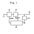
- FIG. 1 of the accompanying drawings shows an ordinary light-receiving circuit incorporating an automatic gain control circuit.
- 11 represents a light signal
- 12 is an avalanche photo diode (APD)
- 13 is an amplifier
- 14 is a level detector
- 15 is the output terminal
- 16 is an AGC circuit.
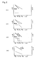
- FIGS 2(1) to 2(3) show the relation between the light input level P, M of the APD 12 and gain G of the amplifier 13 in the methods (a) to (c) given above.
- the solid line indicates M
- the broken line indicates G
- the chained line indicates the optimum value of M as will be explained later.
- M min is the minimum value of the applicable multiplication factor of the APD. When M ⁇ M min , it is not practical because the response speed of the APD becomes very low as a result of an increase of the capacitance.
- SNR signal to noise ratio
- Equation (1) shows that the SNR depends on P and M and the optimum value M o of M gives the maximal point of SNR. From equation (1), the dependency on light input level of M o is expressed as follows. Therefore,
- x is selected as a value ranging from 0.3 to 1.
- the gain G of the amplifier is automatically determined corresponding to M o from the condition that the output of the amplifier is to be maintained at a substantially constant level and the so determined gain is the optimum value.
- the SNR is deteriorated if solely the electrical output signal level is kept at a substantially constant level, since there will be a difference between the M, which keeps the electrical signal at a constant level, and said optimum value M o .
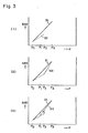
- Figures 3(1), 3(2) and 3(3) show such conditions.
- the figures show the relation between change in light input and the SNR corresponding to the above-mentioned methods (a), (b) and (c).
- the solid line in the figure shows the ideal values, while the broken lines 32, 33, 34 respectively show the value for the gain control methods (a), (b) and (c).
- the solid line 31 and broken lines 32, 33, 34 cross at the point P o
- the solid line 31 and the broken lines 33, 34 cross at the point P 3 since as shown in Figures 2(1), 2(2), 2(3), the curve for M crosses the optimum value M o curve at the points P o and P 3 .
- the value of M is not lowered as far as M min but always kept at a value which is equal to or larger than a value M 1 (>M min ).
- M is limited by M 1 and the SNR is improved.
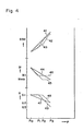
- FIG. 4 together with an example of method (b).
- the solid lines 41, 44 and 47 show the ideal conditions, while the broken lines 42, 45, 48 show the conditions resulting from method (b), and the chained lines 43, 46, 49 show the condition where M is not allowed to fall below M i .
- the present invention seeks to provide a light-receiving circuit without the mentioned disadvantages or with disadvantages to a lesser extent.
- a light-receiving circuit including an avalanche photo diode for receiving a light signal and converting it into an electrical signal and an amplifier for amplifying the electrical signal, wherein, to maintain the amplifier output substantially constant irrespective of variation in the light signal input, means are provided to generate voltage control signals to control both the gain of the amplifier and the multiplying factor of said photo diode, characterised in that said means comprises:
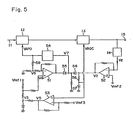
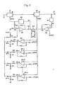
- FIG. 5 is a circuit diagram of one embodiment. of the present invention.
- a light signal input 11 is applied to an avalanche photo diode (APD) 12 and the APD output is amplified by an amplifier 13 and fed to the output terminal 15.
- the output of the amplifier 13 is fed to the level detector 14 and an output voltage V, of the level detector 14 is connected to the inverted input of a 2nd comparator 52, consisting of a differential amplifier.
- a 2nd reference voltage V ref2 is applied to the non-inverted input of the 2nd comparator 52.
- An output voltage V 2 of the 2nd comparator 52 is connected to the AGC control terminal input of the amplifier 13, via the resistor 58, supplying the automatic gain control voltage V AGC thereto.
- the output of the 2nd comparator 52 is also connected to a switch device, consisting of a diode 56, the output of which forms an input voltage V, for a high voltage generator circuit 54.
- An output voltage V APD of the high voltage generator circuit 54 is input to the APD 12 and simultaneously V APD is divided into a voltage V6, via the resistor 59, that is applied to the inverted input of a 1st comparator 51, also consisting of a differential amplifier.
- a voltage V 4 obtained by division from a 1st reference voltage V ref1 is applied.
- An output of the 1st comparator 51 is input to the high voltage generator circuit 54 via a switch device consisting of the diode 55.
- the voltage V AGC is also supplied to the non-inverted input of a 3rd comparator 53, consisting of a differential amplifier, whilst a 3rd reference voltage V ref3 is applied to the inverted input.
- An output voltage V 5 of this 3rd comparator 53 determines a voltage V 4 in combination with the 1st reference voltage V ref1 .
- M is adjusted to the optimum value and the gain G of amplifier 13 is the maximum.
- the output voltage V 2 of the 2nd comparator gradually reduces.
- the voltage V 2 Since the voltage V 2 is at this stage positive, it is applied to the high voltage generator circuit 54 passing the diode 56, and thereby a voltage V APD is obtained as the output of circuit 54.
- the voltage V APD also reduces as the voltage V 2 reduces.
- M of the APD also reduces.
- the voltage V APD reduces until the voltage V 6 divided from the voltage V APD reaches the voltage V 4 divided from the 1st reference voltage V ref1 . This is arranged to occur when the light input level reaches P 2 '. Also, at this light level V 2 changes from positive to negative.
- V 6 reaches the voltage V4
- a positive voltage is output to the output of the 1st comparator and thereby the diode 55 turns ON, forming the loop through the 1st comparator 51 and the high voltage generator circuit 54, keeping the V APD at a constant level. Therefore, the value of M becomes a constant.
- the voltage V 2 is positive until the light input level reaches the point P 2 ' of Fig. 6 as shown above and until this point VAGI is clamped by the diode 57.
- the voltage V AGC reduces and thereby the gain G of the amplifier 13 also reduces.
- voltage V 2 corresponds to the 3rd reference voltage V lef3 .
- the polarity of the output voltage V 5 of the 3rd comparator 53 changes from positive to negative, causing the voltage V 3 to change to negative.
- the output voltage V 5 of comparator 53 reaches a saturation value and stays constant despite further light level increase.
- the voltage V 3 is reduced until the voltage V 5 reaches this negative saturation level.
- the voltage V 4 reduces according to it until a value corresponding to the saturation level of the voltage V 5 .
- the V APD and the value of M reduce in the same way, and when M reaches a constant value corresponding to the saturation level of V 5 , it stays fixed to such a value.
- the V AGC is further reduced and the gain G is also lowered.
- the gain G does, of course, reduce since the V AGC reduces, but the gain reduction is as small as 1/(gain of comparator 53) as compared with variation of M, and therefore the gain is indicated as a constant value for simplification of explanation.
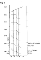
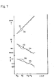
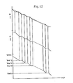
- Figure 7 shows with the solid lines 71, 73, 75, the optimum values of SNR, M and G with varying light input, and also shows the approximate values obtained by the light-receiving circuit of the embodiment of the present invention, by means of the broken lines 72, 74 and 76.
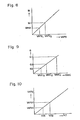
- Figure 8 is a characteristic indicating an example of the relationship between V APD and M of APD 12.
- Figure 9 is a characteristic indicating an example of the relationship between V AGC and the gain G of amplifier 13.
- Figure 10 shows a characteristic indicating the relation between the input voltage V 7 and output voltage V APD of the high voltage generator circuit 54.
- the multiplication factor M of the APD is approximated to the optimum value M o by a polygonal line having three turning points (the gain G is automatically approximated to the ideal condition), but it is also possible to obtain a modification of the embodiment which more approximates the SNR to the optimum value by additionally providing in parallel a plurality of the 3rd comparators as shown in Fig. 11 and by setting the reference voltages corresponding to one 3rd reference voltage of these comparators to different values.
- the comparators 53-1, 53-2 to 53-n are provided in parallel with the comparator 53, and the reference voltages V ref4 , V ref5 to V refn are input to the inverted inputs thereof, whilst V AGC is input to the non-inverted inputs.
- the outputs of the comparators 53-1 to 53-n are connected with the resistors R 4 , R 5 to R “ , diodes D 4 to D n , and diodes D 4-1 to D n-1 .
- the voltages V ref3 , V ref4 , Vref 5 to V refn are in the following relation as while the resistors R 3 , R 4 , R 5 to R " are in the relation as R 3 >R 4 >R 5 >R n .
- the circuit operation is explained below.
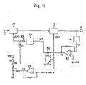
- Figure 13 shows another embodiment of the present invention.
- the circuit indicated has the same function as the circuit shown in Fig. 5.
- the only difference from the circuit of Fig. 5 is that the comparator 51, diode 55 and resistor 59 are removed, and an output of the high voltage generator circuit 54 is connected to the resistor R 2 , which is connected to the reference power supply V ref1 , via the diode D 1 (which forms a first comparator corresponding to 51).
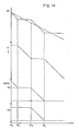
- the Fig. 13 circuit operation will be explained by referring to Fig. 14.
- the output voltage V 2 of the comparator 52 is positive and is applied to the high voltage generator circuit 54 as the voltage V 7 via the diode 56.
- the voltage V 7 is lowered and also the voltage V APD becomes low.
- the voltage V becomes equal to the reference voltage V ref2
- the output voltage V 2 becomes negative and the switch or diode 56 turns OFF and the voltage V APD becomes equal to the voltage V 4 , the voltage V APD is thus clamped to V 4 .
- the present invention provides a light-receiving circuit with a simple structure which can assure wide light input dynamic range without allowing the SNR to be deviated largely from the optimum value and without needing the desired variable gain width of the amplifier to be widened.
Landscapes
- Physics & Mathematics (AREA)
- Electromagnetism (AREA)
- Engineering & Computer Science (AREA)
- Computer Networks & Wireless Communication (AREA)
- Signal Processing (AREA)
- Optical Communication System (AREA)
- Light Receiving Elements (AREA)
Claims (6)
Applications Claiming Priority (2)
| Application Number | Priority Date | Filing Date | Title |
|---|---|---|---|
| JP55085246A JPS5911215B2 (ja) | 1980-06-25 | 1980-06-25 | 光受信回路 |
| JP85246/80 | 1980-06-25 |
Publications (3)
| Publication Number | Publication Date |
|---|---|
| EP0054571A1 EP0054571A1 (de) | 1982-06-30 |
| EP0054571A4 EP0054571A4 (de) | 1982-11-25 |
| EP0054571B1 true EP0054571B1 (de) | 1985-05-08 |
Family
ID=13853203
Family Applications (1)
| Application Number | Title | Priority Date | Filing Date |
|---|---|---|---|
| EP81901676A Expired EP0054571B1 (de) | 1980-06-25 | 1981-06-15 | Licht-empfängerkreis |
Country Status (6)
| Country | Link |
|---|---|
| US (1) | US4495410A (de) |
| EP (1) | EP0054571B1 (de) |
| JP (1) | JPS5911215B2 (de) |
| KR (1) | KR840002284B1 (de) |
| DE (1) | DE3170387D1 (de) |
| WO (1) | WO1982000073A1 (de) |
Families Citing this family (18)
| Publication number | Priority date | Publication date | Assignee | Title |
|---|---|---|---|---|
| JPS60146539A (ja) * | 1984-01-10 | 1985-08-02 | Nec Corp | 光受信器 |
| US4679252A (en) * | 1984-01-11 | 1987-07-07 | Chevron Research Company | Fiber optic receiver having a method and an apparatus for data clock extraction |
| US4688268A (en) * | 1984-01-11 | 1987-08-18 | Chevron Research Company | Fiber optic receiver having a combined baseline clamp and automatic gain control detector |
| JPS61177832A (ja) * | 1985-02-04 | 1986-08-09 | Nippon Telegr & Teleph Corp <Ntt> | 光受信装置の自動利得制御方式 |
| JPS6313534A (ja) * | 1986-07-05 | 1988-01-20 | Nec Corp | バイアス電圧制御回路 |
| EP0282801B1 (de) * | 1987-03-17 | 1992-04-29 | Siemens Aktiengesellschaft | Regelung des Multiplikationsfaktors von Lawinenphotodioden in optischen Empfängern |
| JPS6450112A (en) * | 1987-08-20 | 1989-02-27 | Nec Corp | Dc/dc converting circuit |
| EP0313914B1 (de) * | 1987-10-26 | 1993-03-03 | Siemens Aktiengesellschaft | Schaltungsanordnung mit einem an einen opto-elektrischen Wandler angeschlossenen Vorverstärker |
| JPH01186168A (ja) * | 1988-01-20 | 1989-07-25 | Oki Electric Ind Co Ltd | 受光用高圧発生回路 |
| JPH02113640A (ja) * | 1988-10-21 | 1990-04-25 | Toshiba Corp | 自動利得制御装置 |
| JPH02209029A (ja) * | 1989-02-09 | 1990-08-20 | Toshiba Corp | 自動利得制御装置 |
| JP2713224B2 (ja) * | 1995-05-01 | 1998-02-16 | 日本電気株式会社 | 光受信器 |
| US5929982A (en) * | 1997-02-04 | 1999-07-27 | Tektronix, Inc. | Active APD gain control for an optical receiver |
| US6188059B1 (en) | 1998-01-30 | 2001-02-13 | Sumitomo Electric Industries, Ltd. | Photocurrent monitor circuit and optical receiver |
| US6313459B1 (en) | 2000-05-31 | 2001-11-06 | Nortel Networks Limited | Method for calibrating and operating an uncooled avalanche photodiode optical receiver |
| US20050224697A1 (en) * | 2004-04-08 | 2005-10-13 | Naoki Nishiyama | Light-receiving circuit capable of expanding a dynamic range of an optical input |
| US20070285155A1 (en) * | 2004-08-18 | 2007-12-13 | Shinji Yano | Discrimination Circuit, Gain Adjustment Circuit, Signal Processing Circuit, and Electric Device |
| US9780743B2 (en) * | 2015-10-22 | 2017-10-03 | Google Inc. | Light sensor readout system and method of converting light into electrical signals |
Citations (3)
| Publication number | Priority date | Publication date | Assignee | Title |
|---|---|---|---|---|
| JPS5358748A (en) * | 1976-11-08 | 1978-05-26 | Hitachi Ltd | Light receiving amplifier |
| JPS5359345A (en) * | 1976-09-21 | 1978-05-29 | Post Office | Signal level stabilizer |
| JPS5390802A (en) * | 1977-01-21 | 1978-08-10 | Hitachi Ltd | Control system for light receiving system |
Family Cites Families (2)
| Publication number | Priority date | Publication date | Assignee | Title |
|---|---|---|---|---|
| US4236069A (en) * | 1978-10-16 | 1980-11-25 | Varo, Inc. | Avalanche photodiode gain control system |
| US4399416A (en) * | 1980-11-10 | 1983-08-16 | Texaco Development Corporation | Floating point amplifier |
-
1980
- 1980-06-25 JP JP55085246A patent/JPS5911215B2/ja not_active Expired
-
1981
- 1981-06-11 KR KR1019810002102A patent/KR840002284B1/ko not_active Expired
- 1981-06-15 US US06/349,090 patent/US4495410A/en not_active Expired - Fee Related
- 1981-06-15 DE DE8181901676T patent/DE3170387D1/de not_active Expired
- 1981-06-15 EP EP81901676A patent/EP0054571B1/de not_active Expired
- 1981-06-15 WO PCT/JP1981/000138 patent/WO1982000073A1/ja not_active Ceased
Patent Citations (3)
| Publication number | Priority date | Publication date | Assignee | Title |
|---|---|---|---|---|
| JPS5359345A (en) * | 1976-09-21 | 1978-05-29 | Post Office | Signal level stabilizer |
| JPS5358748A (en) * | 1976-11-08 | 1978-05-26 | Hitachi Ltd | Light receiving amplifier |
| JPS5390802A (en) * | 1977-01-21 | 1978-08-10 | Hitachi Ltd | Control system for light receiving system |
Also Published As
| Publication number | Publication date |
|---|---|
| DE3170387D1 (en) | 1985-06-13 |
| US4495410A (en) | 1985-01-22 |
| JPS5911215B2 (ja) | 1984-03-14 |
| JPS5711548A (en) | 1982-01-21 |
| EP0054571A4 (de) | 1982-11-25 |
| KR840002284B1 (ko) | 1984-12-14 |
| EP0054571A1 (de) | 1982-06-30 |
| KR830007003A (ko) | 1983-10-12 |
| WO1982000073A1 (en) | 1982-01-07 |
Similar Documents
| Publication | Publication Date | Title |
|---|---|---|
| EP0054571B1 (de) | Licht-empfängerkreis | |
| US4438348A (en) | Temperature compensated avalanche photodiode optical receiver circuit | |
| US7265626B2 (en) | Fast-setting digital automatic gain control | |
| US10171057B1 (en) | Automatic gain control loop | |
| US5095542A (en) | Apparatus for controlling transmission output level for burst signal | |
| US11463177B2 (en) | Optic signal receiver with dynamic control | |
| KR100445910B1 (ko) | 광신호 세기의 변동에 관계없이 최적의 수신 성능을 갖는광신호 수신장치 및 그 방법 | |
| EP0058703B1 (de) | Einrichtung zur erhöhung des dynamikbereichs an der eingangsstufe eines empfängers in einem lichtwellenleiter-informationsübertragungssystem | |
| EP0868022B1 (de) | Offsetkorrekturschaltung | |
| US6654215B2 (en) | Photodetector circuit with avalanche photodiode | |
| JPH06103765B2 (ja) | 半導体レーザバイアス電流制御方式 | |
| JPH07264131A (ja) | 光加入者伝送システム及びそのシステムに用いられる加入者ユニット | |
| CN107342741B (zh) | Apd偏压控制电路、光电接收电路以及偏压控制方法 | |
| US4987298A (en) | Automatic gain control apparatus which adjusts bias and gain to maximize signal to noise ratio | |
| US4499609A (en) | Symmetrically clamped fiber optic receiver | |
| US5070516A (en) | Method and apparatus for reducing noise on a signal encodable on a plurality of predetermined levels | |
| JPS623625B2 (de) | ||
| JP2713126B2 (ja) | 光受信装置 | |
| JPH01286655A (ja) | 光受信回路 | |
| JP2008048334A (ja) | 光受信器 | |
| JPS6057726B2 (ja) | 光信号受信器の利得制御方法 | |
| JP2006270616A (ja) | 光受信回路 | |
| JP2002217833A (ja) | 光受信器 | |
| TW202546459A (zh) | 光通訊耦合模塊及其操作方法 | |
| JPH02108349A (ja) | 光受信器 |
Legal Events
| Date | Code | Title | Description |
|---|---|---|---|
| PUAI | Public reference made under article 153(3) epc to a published international application that has entered the european phase |
Free format text: ORIGINAL CODE: 0009012 |
|
| 17P | Request for examination filed |
Effective date: 19820215 |
|
| AK | Designated contracting states |
Designated state(s): DE FR GB NL |
|
| GRAA | (expected) grant |
Free format text: ORIGINAL CODE: 0009210 |
|
| AK | Designated contracting states |
Designated state(s): DE FR GB NL |
|
| REF | Corresponds to: |
Ref document number: 3170387 Country of ref document: DE Date of ref document: 19850613 |
|
| ET | Fr: translation filed | ||
| PLBE | No opposition filed within time limit |
Free format text: ORIGINAL CODE: 0009261 |
|
| STAA | Information on the status of an ep patent application or granted ep patent |
Free format text: STATUS: NO OPPOSITION FILED WITHIN TIME LIMIT |
|
| 26N | No opposition filed | ||
| PGFP | Annual fee paid to national office [announced via postgrant information from national office to epo] |
Ref country code: NL Payment date: 19870630 Year of fee payment: 7 |
|
| PG25 | Lapsed in a contracting state [announced via postgrant information from national office to epo] |
Ref country code: GB Effective date: 19890615 |
|
| PG25 | Lapsed in a contracting state [announced via postgrant information from national office to epo] |
Ref country code: NL Effective date: 19900101 |
|
| GBPC | Gb: european patent ceased through non-payment of renewal fee | ||
| NLV4 | Nl: lapsed or anulled due to non-payment of the annual fee | ||
| PG25 | Lapsed in a contracting state [announced via postgrant information from national office to epo] |
Ref country code: FR Free format text: LAPSE BECAUSE OF NON-PAYMENT OF DUE FEES Effective date: 19900228 |
|
| PG25 | Lapsed in a contracting state [announced via postgrant information from national office to epo] |
Ref country code: DE Effective date: 19900301 |
|
| REG | Reference to a national code |
Ref country code: FR Ref legal event code: ST |