EP0048146A1 - Optisch gekoppelter Festkörper-Schalter - Google Patents
Optisch gekoppelter Festkörper-Schalter Download PDFInfo
- Publication number
- EP0048146A1 EP0048146A1 EP81304179A EP81304179A EP0048146A1 EP 0048146 A1 EP0048146 A1 EP 0048146A1 EP 81304179 A EP81304179 A EP 81304179A EP 81304179 A EP81304179 A EP 81304179A EP 0048146 A1 EP0048146 A1 EP 0048146A1
- Authority
- EP
- European Patent Office
- Prior art keywords
- mosfet
- switch
- gate
- voltage
- turn
- Prior art date
- Legal status (The legal status is an assumption and is not a legal conclusion. Google has not performed a legal analysis and makes no representation as to the accuracy of the status listed.)
- Granted
Links
- 239000007787 solid Substances 0.000 title claims abstract description 17
- 230000008859 change Effects 0.000 claims abstract description 9
- 239000004065 semiconductor Substances 0.000 claims abstract description 6
- 230000005669 field effect Effects 0.000 claims abstract description 4
- 229910044991 metal oxide Inorganic materials 0.000 claims abstract description 3
- 150000004706 metal oxides Chemical class 0.000 claims abstract description 3
- 238000002955 isolation Methods 0.000 claims description 15
- 238000003491 array Methods 0.000 claims description 9
- 230000000694 effects Effects 0.000 claims description 8
- 238000005516 engineering process Methods 0.000 claims description 8
- 230000000903 blocking effect Effects 0.000 claims description 5
- 230000002457 bidirectional effect Effects 0.000 claims description 3
- 230000008878 coupling Effects 0.000 claims description 2
- 238000010168 coupling process Methods 0.000 claims description 2
- 238000005859 coupling reaction Methods 0.000 claims description 2
- 238000005286 illumination Methods 0.000 claims description 2
- 239000007888 film coating Substances 0.000 claims 1
- 238000009501 film coating Methods 0.000 claims 1
- 235000014676 Phragmites communis Nutrition 0.000 description 5
- 238000010586 diagram Methods 0.000 description 4
- 238000013459 approach Methods 0.000 description 3
- 238000004519 manufacturing process Methods 0.000 description 3
- 238000000034 method Methods 0.000 description 3
- 230000003287 optical effect Effects 0.000 description 3
- 230000005855 radiation Effects 0.000 description 3
- 230000009471 action Effects 0.000 description 2
- 230000015556 catabolic process Effects 0.000 description 2
- 238000009792 diffusion process Methods 0.000 description 2
- 230000036039 immunity Effects 0.000 description 2
- 238000012545 processing Methods 0.000 description 2
- 230000002441 reversible effect Effects 0.000 description 2
- 230000001052 transient effect Effects 0.000 description 2
- GYHNNYVSQQEPJS-UHFFFAOYSA-N Gallium Chemical compound [Ga] GYHNNYVSQQEPJS-UHFFFAOYSA-N 0.000 description 1
- 101150068246 V-MOS gene Proteins 0.000 description 1
- 230000003213 activating effect Effects 0.000 description 1
- MDPILPRLPQYEEN-UHFFFAOYSA-N aluminium arsenide Chemical compound [As]#[Al] MDPILPRLPQYEEN-UHFFFAOYSA-N 0.000 description 1
- 230000003416 augmentation Effects 0.000 description 1
- 230000035559 beat frequency Effects 0.000 description 1
- 230000001934 delay Effects 0.000 description 1
- 238000011161 development Methods 0.000 description 1
- 230000018109 developmental process Effects 0.000 description 1
- 230000008030 elimination Effects 0.000 description 1
- 238000003379 elimination reaction Methods 0.000 description 1
- 238000000407 epitaxy Methods 0.000 description 1
- 229910052733 gallium Inorganic materials 0.000 description 1
- 230000001939 inductive effect Effects 0.000 description 1
- 230000003993 interaction Effects 0.000 description 1
- 239000007788 liquid Substances 0.000 description 1
- 239000011159 matrix material Substances 0.000 description 1
- 230000007246 mechanism Effects 0.000 description 1
- 238000001465 metallisation Methods 0.000 description 1
- 238000005272 metallurgy Methods 0.000 description 1
- 230000005693 optoelectronics Effects 0.000 description 1
- 230000010355 oscillation Effects 0.000 description 1
- 230000003071 parasitic effect Effects 0.000 description 1
- 230000008092 positive effect Effects 0.000 description 1
- 230000008569 process Effects 0.000 description 1
- 230000001172 regenerating effect Effects 0.000 description 1
- 230000003252 repetitive effect Effects 0.000 description 1
- 230000004044 response Effects 0.000 description 1
- 229920006395 saturated elastomer Polymers 0.000 description 1
- 229910052710 silicon Inorganic materials 0.000 description 1
- 239000010703 silicon Substances 0.000 description 1
- 230000005236 sound signal Effects 0.000 description 1
- 238000012360 testing method Methods 0.000 description 1
- 238000012546 transfer Methods 0.000 description 1
Images

Classifications
-
- H—ELECTRICITY
- H03—ELECTRONIC CIRCUITRY
- H03K—PULSE TECHNIQUE
- H03K17/00—Electronic switching or gating, i.e. not by contact-making and –breaking
- H03K17/51—Electronic switching or gating, i.e. not by contact-making and –breaking characterised by the components used
- H03K17/78—Electronic switching or gating, i.e. not by contact-making and –breaking characterised by the components used using opto-electronic devices, i.e. light-emitting and photoelectric devices electrically- or optically-coupled
- H03K17/79—Electronic switching or gating, i.e. not by contact-making and –breaking characterised by the components used using opto-electronic devices, i.e. light-emitting and photoelectric devices electrically- or optically-coupled controlling bipolar semiconductor switches with more than two PN-junctions, or more than three electrodes, or more than one electrode connected to the same conductivity region
-
- H—ELECTRICITY
- H01—ELECTRIC ELEMENTS
- H01L—SEMICONDUCTOR DEVICES NOT COVERED BY CLASS H10
- H01L31/00—Semiconductor devices sensitive to infrared radiation, light, electromagnetic radiation of shorter wavelength or corpuscular radiation and specially adapted either for the conversion of the energy of such radiation into electrical energy or for the control of electrical energy by such radiation; Processes or apparatus specially adapted for the manufacture or treatment thereof or of parts thereof; Details thereof
- H01L31/12—Semiconductor devices sensitive to infrared radiation, light, electromagnetic radiation of shorter wavelength or corpuscular radiation and specially adapted either for the conversion of the energy of such radiation into electrical energy or for the control of electrical energy by such radiation; Processes or apparatus specially adapted for the manufacture or treatment thereof or of parts thereof; Details thereof structurally associated with, e.g. formed in or on a common substrate with, one or more electric light sources, e.g. electroluminescent light sources, and electrically or optically coupled thereto
- H01L31/16—Semiconductor devices sensitive to infrared radiation, light, electromagnetic radiation of shorter wavelength or corpuscular radiation and specially adapted either for the conversion of the energy of such radiation into electrical energy or for the control of electrical energy by such radiation; Processes or apparatus specially adapted for the manufacture or treatment thereof or of parts thereof; Details thereof structurally associated with, e.g. formed in or on a common substrate with, one or more electric light sources, e.g. electroluminescent light sources, and electrically or optically coupled thereto the semiconductor device sensitive to radiation being controlled by the light source or sources
- H01L31/167—Semiconductor devices sensitive to infrared radiation, light, electromagnetic radiation of shorter wavelength or corpuscular radiation and specially adapted either for the conversion of the energy of such radiation into electrical energy or for the control of electrical energy by such radiation; Processes or apparatus specially adapted for the manufacture or treatment thereof or of parts thereof; Details thereof structurally associated with, e.g. formed in or on a common substrate with, one or more electric light sources, e.g. electroluminescent light sources, and electrically or optically coupled thereto the semiconductor device sensitive to radiation being controlled by the light source or sources the light sources and the devices sensitive to radiation all being semiconductor devices characterised by at least one potential or surface barrier
-
- H—ELECTRICITY
- H03—ELECTRONIC CIRCUITRY
- H03K—PULSE TECHNIQUE
- H03K17/00—Electronic switching or gating, i.e. not by contact-making and –breaking
- H03K17/51—Electronic switching or gating, i.e. not by contact-making and –breaking characterised by the components used
- H03K17/78—Electronic switching or gating, i.e. not by contact-making and –breaking characterised by the components used using opto-electronic devices, i.e. light-emitting and photoelectric devices electrically- or optically-coupled
- H03K17/785—Electronic switching or gating, i.e. not by contact-making and –breaking characterised by the components used using opto-electronic devices, i.e. light-emitting and photoelectric devices electrically- or optically-coupled controlling field-effect transistor switches
Definitions
- This invention relates to solid state optically coupled switches.
- switches can be characterized as solid state relays (SSR's) or analog switches.
- LED light-emitting diode
- couplers While the primary purpose of couplers is only to isolate, the purpose of reed relays and SSR's is not only to isolate but also to provide power gain.
- couplers generally are limited in current and voltage. They are usually limited to DC loads and are particularly susceptible to damage when switching inductive loads or when operating in an overload current mode. Furthermore, they exhibit a voltage offset of about one volt because of the use of bipolar photo-semiconductors. This means that voltages under one volt cannot be switched and that audio signals cannot be faithfully reproduced without the use of biasing.
- SSR's can offer considerable power gain and isolation, they are generally relegated to being designed for AC or DC operation, but not both. Also, an AC load SSR employing a thyristor as the output element is subject to false latchup. In any event, such an SSR is not capable of being turned off in mid-cycle.
- Reed relays experience difficulties with reactive loads and, although faster than conventional mechanical relays, are still slower than solid state switches. Also, reed relays are limited in the degree they can switch momentarily high currents or voltages. Finally, under very high switching rates, their mechanical life has a severe limitation.
- FET field effect transistors
- the invention accordingly provides a solid state optically coupled electrical switch wherein light from a solid state light emitter (L-l) is coupled refractively to a solid state, photovoltaic series diode array (D-V) laterally through a thin, clear film so as to act as a DC-to-DC transformer and create a voltage, and wherein such voltage is applied to a metal oxide semiconductor field effect transistor (MOSFET) (Q-1) having a gate, a source and a drain, between the gate and source and cause the MOSFET to change from a first impedance state to a second impedance state.
- MOSFET metal oxide semiconductor field effect transistor
- a diode (LED) chip constituting the light emitter can be placed adjacent to an integrated circuit sensor chip constituting the photovoltaic array.
- the photovoltaic array When activated by light from the LED, the photovoltaic array can create a voltage of at least 8 volts. This voltage, applied between the source and gate of the power MOSFET transistor causes the transistor's impedance to change from many megohms down to a few ohms.
- the light emitter may consist of a liquid epitaxy gallium or gallium aluminum arsenide LED to provide greater brightness than a simple diffused LED.
- the photovoltaic array may contain 16 diodes connected in series with connections at either end or at the midpoint of the series string.
- the sensor diode array can be fabricated using dielectric isolation techniques. This eliminates parasitic light-generated voltages which could exist at various PN junctions if conventional isolation-diffusion integrated circuit processing were used. ' A low voltage MOSFET may be used to enhance the overall switching speed.
- Light is coupled from the LED to the sensor through a thin, clear film. Coupling is by refractive means, as described in U.S. Patent Application 065 072 filed 9 August 1979, the disclosure of which is incorporated herein by reference.
- the diode string or array when activated by light, generates slightly more than 0.5 volts per diode, or slightly above 8 volts total.
- the sensor chip size can be chosen so as to deliver only several microamperes, through larger chips could, of course, deliver more current. However, relatively low current is adequate to drive the gate of the FET because of its high input impedance.
- the MOSFET may be an enhancement mode or a depletion mode MOSFET, the switching of the latter from a low to a high impedance state affording normally closed relay-contact behaviour analogous to that of normally closed relays.
- Two of the MOSFETs can be employed, the voltage generated at the photovoltaic array (D-V) by the light-emitter (L-1) being simultaneously applied between the gate and source of each MOSFET, the MOSFETs being connected in series opposition with common sources and common gates, and being of a structure that permits them to withstand off-state voltages of more than a few volts in one direction.
- the series-opposition connection permits one MOSFET to sustain off-state voltage regardless of the output voltage polarity.
- both MOSFETs change from a high to a low impedance to provide as a net result an optically coupled AC switch.
- the diode array can be directly coupled to the MOSFET without blocking or steering diodes or the like.
- the siwtch is thereby capable of switching AC or DC; it does not exhibit voltage offset and thereby readily switches AC voltages of the order of a hundred millivolts.
- the MOSFET can be such that its turn-on and turn-off speeds are limited by the time taken for the gate capacitance to charge from the photovoltaic diode voltage or discharge through the equivalent gate source impedance.
- This length of switching time has the positive effect of essentially limiting circuit turn-on rate of change of current with time (di/dt) and turn-off rate of change of voltage with time (dv/dt) and prevents the generation of switching-induced radio frequency interference (RFI) regardless of load power factor, an attribute not readily feasible with conventional FRI- reducing, zero-voltage or zero-current axis thyristor switching circuits.
- the switch of the invention can include a second photovoltaic array (D-V 2 ) and a second depletion mode MOSFET (Q-2), and wherein each of a pair of the depletion mode MOSFETs is activated by a respective one of the photovoltaic arrays in a mutually exclusive manner such that one or the other MOSFET is turned off, and wherein depletion-FET circuit configurations are used whereby the switch is more readily turned off than turned on. Turn-off then is faster than turn-on, whereby an operation of single-pole, double throw, break-before-make operation analogous to mechanical relay configuration Form C is achieved in a solid state switching apparatus.
- D-V 2 second photovoltaic array
- Q-2 second depletion mode MOSFET
- the diodes of the diode array are located around the light-emitter so as to be equally illuminated thereby, and the invention also provides a series array of dielectrically isolated photovoltaic diodes fabricated in a wagon wheel spoke geometry and coated with a hemispherical clear film such that a light emitter located centrally of the photovoltaic array illuminates all diodes substantially equally.
- the invention additionally provides a photovoltaically activated bidirectional FET switch wherein a pair of output FETs is activated by a fixed power supply connected to their gates and sources through a photovolatically activated, low current, low capacitance, high speed FET whereby the output FETs experience rapid charging of their gate-source capacitances and corresponding rapid turn-on, with the output FET handling load current and the driver FET being of a low input capacitance type and each of the two FETs being driven by separate photovoltaic generators which are activated by the same light sources, to thereby effect rapid charging of the output device gate-source capacitance and resultant turn-on.
- FET technology is combined with certain optoelectronic means alone or supplemented by electromagnetic means to achieve both superior switching characteristics and fabrication means compatible with low-cost mass production.
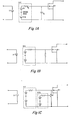
- Fig. 1A shows a simple form of switch embodying the invention in which an LED L-1 when activated by a control current of about 10 mA generates infrared radiation which is sensed simultaneously by all the diodes of an integrated diode array D-V comprising sixteen series connected diodes.
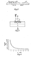
- Fig. 2 depicts the light path by which the radiation from the LED L-1 is refractively coupled with the diodes, by way of a thin clear film.
- the output of the array D-V is connected as shown to the gate and source of a MOSFET Q-1, the geometry of which is shown in cross-section in Fig. 3.
- MOSFET Q-1 exhibits an equivalent capacitance C E between its gate and source, which is of the order of several dozen picofarads for a chip 0.050 inches by 0.050 inches 1.27 mm. by 1.27 mm.
- the capacitance C E charges to the voltage generated through the D-V series equivalent resistance R E which, for a sensor chip of about 0.040 inches by 0.040 inches (1.01 mm. by 1.01 mm.), is about 1 Megohm.
- the turn-on time for the MOSFET Q-1 is the time it takes for the capacitance C E to charge to a high enough voltage for the MOSFET to have approached its lowest ON resistance.
- the two R E /C E time constants put the MOSFET Q-1 gate voltage above 6 volts, a value where Q-1 is essentially full on.
- Fig. 4 depicts the effect of gate voltage V Q on ON resistance.
- capacitance C E It may take, for example, about 20-50 microseconds to charge capacitance C E and turn on the MOSFET Q-1.
- the diode array D-V stops generating a voltage.
- the charge remains on the capacitance C E , thereby holding the MOSFET Q-1 on until stray leakage paths eventually discharge the capacitance C E . Since several seconds could be required for discharge, alternate means for faster turn-off are normally required.
- the ideal arrangement is one where the full D-V voltage is applied during turn-on with minimal biasing, but where maximum biasing is attained during turn-off.
- Such an arrangement is provided in the switch circuit illustrated in Fig. 1C, where the bias resistor of Fig. 1B is replaced by an P-channel depletion mode junction FET Q-2.
- -A second diode array D-V 2 is connected to the gate of FET Q-2.
- FET Q-2 being a depletion mode FET, is normally in a low impedance state, well under 1,000 ohms.
- the photovoltaic diode generators or arrays D-V and D-V and the FET Q-2 are fabricated on the same chip using dielectric isolation. Each diode is electrically isolated from the next except for surface interconnect metallurgy, which proceeds from one anode to the next cathode.
- the oxide "tub" surrounding each diode prevents electrical interaction except between the P and N regions of each diode through surface interconnect metalization.
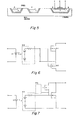
- Fig. 5 depicts the cross-sectional geometry of the diodes and the bias FET Q-2. While Figs. lA, 1B and 1C reflect basic configurations, an embodiment of the invention better suited for many practical applications is shown in Fig. 6.
- the voltage generated by diode array D-V is simultaneously applied to the gates and sources of FETs Q-1 and Q-2, which are connected source-to-source.
- FETs Q-1 and Q-2 can each block voltage in one direction, but can withstand only about one volt in the reverse direction.
- either Q-1 or Q-2 is always in the full blocking mode, thereby blocking load voltage regardless of the polarity.
- LED L-1 is so arranged as to simultaneously activate diode arrays D-V and D-V 2 .
- the consequential reduced impedance of FET Q-2 causes FET Q-1 gate capacitance to suddenly begin charging toward the Hocking voltage through FET Q-2.
- FET Q-2 has an input capacitance much smaller than that of Q-1 by an order of magnitude equal to the degree of turn-on speed enhancement. Since Q-2 handles negligible current, it can be a much smaller chip than Q-1, thereby facilitating a geometry contributing less capacitance.
- the single chip would include the photovoltaic diodes.
- the circuit of Fig. 8 comprises a unique configuration in which transformer action augments the isolated photovoltaic drive scheme in order to achieve very fast turn-on and turn-off times.
- LED L-1 is in parallel with the primary of a pulse transformer T-1.
- LED L-1 is illuminated. This would normally cause voltage generator or diode array D -V to begin charging C E , in turn causing FET Q-1 to turn on in a time comparable to the time constant of C E and the internal equivalent resistance.
- the rise in input signal is seen at the secondary of T-1 as a positive pulse which rapidly charges C E through a forward biased zener diode, D Z .
- the positive pulse at the T-1 secondary disappears, but the charge on C E in maintained by the diode array D-V.
- the zener diode D Z be specified at a voltage approximately equal to that of the photovoltaic generator or diode array D-V and that the voltage appearing at the secondary of transformer T-1, especially at turn-off, be greater than the breakdown voltage of this zener diode.
- the result is a magnetically and optically isolated switch capable of switching speeds on the order of hundreds of nanoseconds or better. Since the transformer T-1 is needed only during switching and the switch depends on diode array D-V during the on period, the transformer can be small in size.
- a DC voltage could be used to operate an oscillator.
- the oscillator's high frequency output could be transformer coupled, rectified, filtered and applied to a transistor base or FET gate to turn it on.
- circuits of Figs. 1, 6, 7 and 8 provide simplified switching without the hazard of spurious signals or beat frequencies.
- the maximum output current can be no greater than the current generated by the least illuminated diode in the series array.
- the diode farthest from the LED becomes a limiting factor.
- the diode area should be larger as its distance from the LED increases.
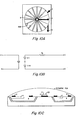
- Fig. 10A The optimized configuration, then, for a series string of photovoltaic diodes is the "wagon wheel” configuration shown in Fig. 10A, with the LED mounted centrally so as to illuminate all the diodes equally.
- Fig. 10B shows the circuit of the configuration of Fig. 10A, Ro being the series equivalent resistance of the array.
- the wagon wheel surface geometry, coupled with the hemispherical refractive film, shown in Fig. 10C, provides maximum response to the LED hemispherical radiation pattern across the entire surface of each diode.
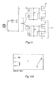
- Fig. 11 depicts such a circuit, capable of switching AC or DC, in which the switching elements are depletion mode V-MOS chips.
- Bias resistors R-1 and R-2 are selected to be above 5 megohm. The result is that when diode arrays or photovoltaic generators DV-1 or DV-2 are activated, turnoff is rapid because of minimum shunt resistance. Turn-on is slower because of the slow discharge of MOSFET gate capacitance through the large bias resistor value.
- LED L ⁇ 1 is normally on, thereby maintaining Q-2 and Q-2 in an OFF condition.
- Q-1 becomes saturated, thereby shunting current around L-1.
- Base current to Q-1 passes through L-2, thereby rapidly turning off Q-4 and Q-5 before Q-2 and Q-3 turn on.
- L-1 initiates rapid turn off of Q-2 and Q-3 before Q-4 and Q-5 turn on.
- Fig. 11A shows the equivalent circuit for such a physical circuit as is shown in Fig. 11.
Applications Claiming Priority (2)
| Application Number | Priority Date | Filing Date | Title |
|---|---|---|---|
| US06/186,419 US4390790A (en) | 1979-08-09 | 1980-09-12 | Solid state optically coupled electrical power switch |
| US186419 | 1994-01-28 |
Publications (2)
| Publication Number | Publication Date |
|---|---|
| EP0048146A1 true EP0048146A1 (de) | 1982-03-24 |
| EP0048146B1 EP0048146B1 (de) | 1986-07-23 |
Family
ID=22684881
Family Applications (1)
| Application Number | Title | Priority Date | Filing Date |
|---|---|---|---|
| EP81304179A Expired EP0048146B1 (de) | 1980-09-12 | 1981-09-11 | Optisch gekoppelter Festkörper-Schalter |
Country Status (5)
| Country | Link |
|---|---|
| US (1) | US4390790A (de) |
| EP (1) | EP0048146B1 (de) |
| JP (1) | JPS57107633A (de) |
| CA (1) | CA1175115A (de) |
| DE (1) | DE3174975D1 (de) |
Cited By (13)
| Publication number | Priority date | Publication date | Assignee | Title |
|---|---|---|---|---|
| FR2538640A1 (fr) * | 1982-12-23 | 1984-06-29 | Fairchild Camera Instr Co | Interrupteur haute tension a semi-conducteurs |
| EP0174073A2 (de) * | 1984-09-03 | 1986-03-12 | Kabushiki Kaisha Toshiba | Integrierte optoelektrische Anordnung |
| FR2587841A1 (fr) * | 1985-09-24 | 1987-03-27 | Efcis | Composant semi-conducteur de puissance et logique de commande associee |
| FR2590750A1 (fr) * | 1985-11-22 | 1987-05-29 | Telemecanique Electrique | Dispositif de commutation de puissance a semi-conducteurs et son utilisation a la realisation d'un relais statique en courant alternatif |
| EP0226395A2 (de) * | 1985-12-04 | 1987-06-24 | Nec Corporation | Festkörperrelais mit einer Thyristor-Entladeschaltung |
| EP0244394A2 (de) * | 1986-04-23 | 1987-11-04 | AVL Medical Instruments AG | Sensorelement zur Bestimmung von Stoffkonzentrationen |
| US4859875A (en) * | 1987-08-28 | 1989-08-22 | Siemens Aktiengesellschaft | Optocoupler for power FET |
| EP0393876A2 (de) * | 1989-04-14 | 1990-10-24 | Hewlett-Packard Company | Hochleistungs-Halbleiterrelais |
| EP0398246A2 (de) * | 1989-05-17 | 1990-11-22 | Kabushiki Kaisha Toshiba | Photokopplerapparat zur Verkürzung der Schaltzeiten der Ausgangskontakte |
| WO2000065718A1 (fr) * | 1999-04-22 | 2000-11-02 | Zhongdu Liu | Interrupteur electrique a l'etat solide a deux extremites |
| GB2352809A (en) * | 1999-08-06 | 2001-02-07 | Matsushita Electric Works Ltd | Illumination sensor and electronic automatic on/off switch |
| EP2045920A1 (de) | 2007-09-26 | 2009-04-08 | Sharp Kabushiki Kaisha | Schaltkreis mit niedriger Schwellenspannung |
| CN104836560A (zh) * | 2015-05-21 | 2015-08-12 | 遵义长征电器防爆设备有限责任公司 | 具有能量回收利用功能的固态继电器 |
Families Citing this family (60)
| Publication number | Priority date | Publication date | Assignee | Title |
|---|---|---|---|---|
| JPS59125140U (ja) * | 1983-02-08 | 1984-08-23 | 横河電機株式会社 | アナログスイツチ |
| DE3311489A1 (de) * | 1983-03-29 | 1984-10-11 | Siemens AG, 1000 Berlin und 8000 München | Vorrichtung zur erzeugung einer gate-vorspannung an feldeffekttransistoren |
| US4564770A (en) * | 1983-03-29 | 1986-01-14 | Rca Corporation | Solid state relay with fast turnoff |
| JPS6014536U (ja) * | 1983-07-08 | 1985-01-31 | 横河電機株式会社 | スイツチ回路 |
| US4568834A (en) * | 1983-09-02 | 1986-02-04 | The United States Of America As Represented By The Secretary Of The Army | High voltage solid state multiplexer |
| DE3344428A1 (de) * | 1983-12-08 | 1985-06-20 | Siemens AG, 1000 Berlin und 8000 München | Schaltungsanordnung mit einem fototransistor |
| GB2154820B (en) * | 1984-01-23 | 1988-05-25 | Int Rectifier Corp | Photovoltaic relay |
| US4777387A (en) * | 1984-02-21 | 1988-10-11 | International Rectifier Corporation | Fast turn-off circuit for photovoltaic driven MOSFET |
| JPS60170322A (ja) * | 1984-01-23 | 1985-09-03 | インターナショナル・レクチフアイヤー・コーポレーション | 固体素子リレー回路 |
| JPS60165116A (ja) * | 1984-02-07 | 1985-08-28 | Chino Works Ltd | スイツチ駆動回路 |
| US4581540A (en) * | 1984-03-16 | 1986-04-08 | Teledyne Industries, Inc. | Current overload protected solid state relay |
| US4665316A (en) * | 1984-11-21 | 1987-05-12 | Telmos Incorporated | Photovoltaic relay switch |
| JPS61219184A (ja) * | 1985-03-25 | 1986-09-29 | Matsushita Electric Works Ltd | 半導体装置 |
| US4647794A (en) * | 1985-05-22 | 1987-03-03 | Teledyne Industries, Inc. | Solid state relay having non overlapping switch closures |
| JPH07120817B2 (ja) * | 1985-07-25 | 1995-12-20 | 松下電工株式会社 | ソリッドステートリレー |
| US4804866A (en) * | 1986-03-24 | 1989-02-14 | Matsushita Electric Works, Ltd. | Solid state relay |
| JP2503417B2 (ja) * | 1986-05-07 | 1996-06-05 | オムロン株式会社 | ソリツドステ−トリレ− |
| US4801822A (en) * | 1986-08-11 | 1989-01-31 | Matsushita Electric Works, Ltd. | Semiconductor switching circuit |
| JPH073881B2 (ja) * | 1986-08-13 | 1995-01-18 | 株式会社東芝 | 光電変換装置 |
| JPS6351681A (ja) * | 1986-08-20 | 1988-03-04 | Agency Of Ind Science & Technol | 半導体装置 |
| JPH01137824A (ja) * | 1987-11-25 | 1989-05-30 | Matsushita Electric Works Ltd | スイッチング装置 |
| JPH0188528U (de) * | 1987-12-03 | 1989-06-12 | ||
| US4871920A (en) * | 1988-04-18 | 1989-10-03 | General Electric Company | High power wide band amplifier using optical techniques and impedance matching to source and load |
| US4939375A (en) * | 1988-06-17 | 1990-07-03 | Hewlett-Packard Company | Solid state relay with shield means |
| US4864126A (en) * | 1988-06-17 | 1989-09-05 | Hewlett-Packard Company | Solid state relay with optically controlled shunt and series enhancement circuit |
| US5223446A (en) * | 1988-11-30 | 1993-06-29 | Sharp Kabushiki Kaisha | Semiconductor device with a photodetector switching device grown on a recrystallized monocrystal silicon film |
| JPH0748559B2 (ja) * | 1988-11-30 | 1995-05-24 | シャープ株式会社 | 半導体装置 |
| US4931778A (en) * | 1989-02-27 | 1990-06-05 | Teledyne Industries, Inc. | Circuitry for indicating the presence of an overload or short circuit in solid state relay circuits |
| US5057694A (en) * | 1989-03-15 | 1991-10-15 | Matsushita Electric Works, Ltd. | Optoelectronic relay circuit having charging path formed by a switching transistor and a rectifying diode |
| JP2555887B2 (ja) * | 1989-06-19 | 1996-11-20 | 日本電気株式会社 | トランスファー型ソリッドステートリレー |
| DE59008698D1 (de) * | 1989-09-07 | 1995-04-20 | Siemens Ag | Optokoppler. |
| US5045680A (en) * | 1990-01-18 | 1991-09-03 | International Business Machines Corporation | Integrated circuit optoelectronic toggle F/F |
| US5151602A (en) * | 1990-02-15 | 1992-09-29 | Matsushita Electric Works, Ltd. | Semiconductor relay circuit using photovoltaic diodes |
| US5138177A (en) * | 1991-03-26 | 1992-08-11 | At&T Bell Laboratories | Solid-state relay |
| US5278422A (en) * | 1991-09-02 | 1994-01-11 | Matsushita Electric Works, Ltd. | Normally open solid state relay with minimized response time of relay action upon being turned off |
| US5225687A (en) * | 1992-01-27 | 1993-07-06 | Jason Barry L | Output circuit with optically coupled control signals |
| DE4206393C2 (de) * | 1992-02-29 | 1995-05-18 | Smi Syst Microelect Innovat | Halbleiterrelais und Verfahren zu seiner Herstellung |
| DE59208693D1 (de) * | 1992-09-24 | 1997-08-14 | Siemens Ag | Leistungsschalter mit strombegrenzender Induktivität |
| JPH06177418A (ja) * | 1992-12-04 | 1994-06-24 | Toshiba Corp | ホトカプラ装置 |
| JP2807388B2 (ja) * | 1993-03-19 | 1998-10-08 | 株式会社東芝 | フォトカプラ装置 |
| US5532498A (en) * | 1994-12-06 | 1996-07-02 | At&T Corp. | High sensitivity control circuit for optical solid-state relays |
| US5549762A (en) * | 1995-01-13 | 1996-08-27 | International Rectifier Corporation | Photovoltaic generator with dielectric isolation and bonded, insulated wafer layers |
| US5910738A (en) * | 1995-04-07 | 1999-06-08 | Kabushiki Kaisha Toshiba | Driving circuit for driving a semiconductor device at high speed and method of operating the same |
| DE19534045A1 (de) * | 1995-09-14 | 1997-03-20 | Cafer Borucu | Elektronisches Relais |
| US6054365A (en) | 1998-07-13 | 2000-04-25 | International Rectifier Corp. | Process for filling deep trenches with polysilicon and oxide |
| US6288458B1 (en) * | 1999-09-30 | 2001-09-11 | Honeywell International Inc. | Power stealing solid state switch |
| US6608445B2 (en) | 2001-12-12 | 2003-08-19 | Honeywell International Inc. | Efficient solid state switching and control system for retractable aircraft landing lights |
| KR100480727B1 (ko) * | 2002-11-26 | 2005-04-07 | 엘지전자 주식회사 | 건조기의 히터 제어장치 |
| US7217915B2 (en) * | 2004-05-07 | 2007-05-15 | Sun Microsystems, Inc. | Method and apparatus for detecting the position of light which is incident to a semiconductor die |
| JP2006186344A (ja) * | 2004-12-02 | 2006-07-13 | Toshiba Corp | 光結合装置 |
| US7480126B2 (en) * | 2005-04-27 | 2009-01-20 | National Instruments Corporation | Protection and voltage monitoring circuit |
| FR2917851B1 (fr) | 2007-06-19 | 2009-08-21 | Schneider Electric Ind Sas | Module d'entrees analogiques isolees a faible courant de fuite. |
| JP5084379B2 (ja) * | 2007-07-12 | 2012-11-28 | 富士通コンポーネント株式会社 | 信号検出回路および信号検出方法、ならびに状態検出回路 |
| US20100186795A1 (en) | 2009-01-28 | 2010-07-29 | Stephen Joseph Gaul | Connection systems and methods for solar cells |
| US20100191383A1 (en) * | 2009-01-28 | 2010-07-29 | Intersil Americas, Inc. | Connection systems and methods for solar cells |
| CN101814527A (zh) * | 2010-04-22 | 2010-08-25 | 复旦大学 | 一种使用光电子注入进行电导调制的功率器件与方法 |
| TWI511450B (zh) * | 2012-07-25 | 2015-12-01 | Himax Analogic Inc | 開關電路 |
| JP5563050B2 (ja) * | 2012-12-10 | 2014-07-30 | 株式会社東芝 | ゲート駆動回路、およびパワー半導体モジュール |
| JP6253439B2 (ja) * | 2014-02-17 | 2017-12-27 | ルネサスエレクトロニクス株式会社 | 半導体装置 |
| CN105245090B (zh) * | 2015-11-11 | 2017-09-15 | 重庆理工大学 | 基于红外隔离通信的开关式功率变换模块的驱动电路 |
Citations (7)
| Publication number | Priority date | Publication date | Assignee | Title |
|---|---|---|---|---|
| US3480783A (en) * | 1966-08-01 | 1969-11-25 | Hughes Aircraft Co | Photon coupler having radially-disposed,serially connected diodes arranged as segments of a circle |
| US3976877A (en) * | 1974-02-22 | 1976-08-24 | U.S. Philips Corporation | Opto-electronic photocoupling device and method of manufacturing same |
| US4124860A (en) * | 1975-02-27 | 1978-11-07 | Optron, Inc. | Optical coupler |
| GB2017297A (en) * | 1978-03-23 | 1979-10-03 | Western Electric Co | Optically Sensitive Switch |
| US4179619A (en) * | 1977-12-02 | 1979-12-18 | General Electric Company | Optocoupler having internal reflection and improved isolation capabilities |
| DE3000890A1 (de) * | 1979-02-21 | 1980-09-04 | Gen Electric | Festkoerperrelais |
| WO1981000493A1 (en) * | 1979-07-30 | 1981-02-19 | Western Electric Co | Optically triggered linear bilateral switch |
Family Cites Families (6)
| Publication number | Priority date | Publication date | Assignee | Title |
|---|---|---|---|---|
| DE1264513C2 (de) * | 1963-11-29 | 1973-01-25 | Texas Instruments Inc | Bezugspotentialfreier gleichstromdifferenzverstaerker |
| US3524986A (en) * | 1967-02-06 | 1970-08-18 | Gen Electric | Semiconductor light gating of light activated semiconductor power control circuits |
| JPS5115368A (de) * | 1974-07-29 | 1976-02-06 | Hitachi Ltd | |
| JPS5462754A (en) * | 1977-10-28 | 1979-05-21 | Fuji Electric Co Ltd | Signal stansmission circuit using photocoupler |
| JPS53166368U (de) * | 1978-05-16 | 1978-12-26 | ||
| US4307298A (en) * | 1980-02-07 | 1981-12-22 | Bell Telephone Laboratories, Incorporated | Optically toggled bilateral switch having low leakage current |
-
1980
- 1980-09-12 US US06/186,419 patent/US4390790A/en not_active Ceased
-
1981
- 1981-09-09 CA CA000385527A patent/CA1175115A/en not_active Expired
- 1981-09-11 DE DE8181304179T patent/DE3174975D1/de not_active Expired
- 1981-09-11 EP EP81304179A patent/EP0048146B1/de not_active Expired
- 1981-09-11 JP JP56143698A patent/JPS57107633A/ja active Granted
Patent Citations (7)
| Publication number | Priority date | Publication date | Assignee | Title |
|---|---|---|---|---|
| US3480783A (en) * | 1966-08-01 | 1969-11-25 | Hughes Aircraft Co | Photon coupler having radially-disposed,serially connected diodes arranged as segments of a circle |
| US3976877A (en) * | 1974-02-22 | 1976-08-24 | U.S. Philips Corporation | Opto-electronic photocoupling device and method of manufacturing same |
| US4124860A (en) * | 1975-02-27 | 1978-11-07 | Optron, Inc. | Optical coupler |
| US4179619A (en) * | 1977-12-02 | 1979-12-18 | General Electric Company | Optocoupler having internal reflection and improved isolation capabilities |
| GB2017297A (en) * | 1978-03-23 | 1979-10-03 | Western Electric Co | Optically Sensitive Switch |
| DE3000890A1 (de) * | 1979-02-21 | 1980-09-04 | Gen Electric | Festkoerperrelais |
| WO1981000493A1 (en) * | 1979-07-30 | 1981-02-19 | Western Electric Co | Optically triggered linear bilateral switch |
Non-Patent Citations (2)
| Title |
|---|
| DESIGN ENGINEERING, Vol. 52, No. 3, March 1981 Waseca V. COUGHLIN et al. "Solid State Relays Meet OEM Requirements" pages 61 to 64 * |
| ELECTRONIC DESIGN, Vol. 28, No. 7, 29 March 1980 Rochelle Park E.T. RODRIGUEZ "Fast DMOS Optocouplers Beat SSRs in Speed and Reed Relays in Performance" pages 60 to 63 * |
Cited By (23)
| Publication number | Priority date | Publication date | Assignee | Title |
|---|---|---|---|---|
| FR2538640A1 (fr) * | 1982-12-23 | 1984-06-29 | Fairchild Camera Instr Co | Interrupteur haute tension a semi-conducteurs |
| EP0174073A2 (de) * | 1984-09-03 | 1986-03-12 | Kabushiki Kaisha Toshiba | Integrierte optoelektrische Anordnung |
| EP0174073A3 (en) * | 1984-09-03 | 1986-12-17 | Kabushiki Kaisha Toshiba | Integrated optical and electric circuit device |
| US4667212A (en) * | 1984-09-03 | 1987-05-19 | Kabushiki Kaisha Toshiba | Integrated optical and electric circuit device |
| FR2587841A1 (fr) * | 1985-09-24 | 1987-03-27 | Efcis | Composant semi-conducteur de puissance et logique de commande associee |
| EP0220974A1 (de) * | 1985-09-24 | 1987-05-06 | STMicroelectronics S.A. | Leistungshalbleiterbauteil und damit verbundene Steuerlogik |
| FR2590750A1 (fr) * | 1985-11-22 | 1987-05-29 | Telemecanique Electrique | Dispositif de commutation de puissance a semi-conducteurs et son utilisation a la realisation d'un relais statique en courant alternatif |
| EP0226395A3 (en) * | 1985-12-04 | 1989-04-19 | Nec Corporation | Solid state relay having a thyristor discharge circuit |
| EP0226395A2 (de) * | 1985-12-04 | 1987-06-24 | Nec Corporation | Festkörperrelais mit einer Thyristor-Entladeschaltung |
| EP0244394A2 (de) * | 1986-04-23 | 1987-11-04 | AVL Medical Instruments AG | Sensorelement zur Bestimmung von Stoffkonzentrationen |
| EP0244394A3 (en) * | 1986-04-23 | 1989-04-19 | Avl Ag | Sensor element for determining the concentration of substances |
| US4859875A (en) * | 1987-08-28 | 1989-08-22 | Siemens Aktiengesellschaft | Optocoupler for power FET |
| EP0393876A3 (de) * | 1989-04-14 | 1991-04-03 | Hewlett-Packard Company | Hochleistungs-Halbleiterrelais |
| EP0393876A2 (de) * | 1989-04-14 | 1990-10-24 | Hewlett-Packard Company | Hochleistungs-Halbleiterrelais |
| EP0398246A2 (de) * | 1989-05-17 | 1990-11-22 | Kabushiki Kaisha Toshiba | Photokopplerapparat zur Verkürzung der Schaltzeiten der Ausgangskontakte |
| EP0398246A3 (de) * | 1989-05-17 | 1993-07-21 | Kabushiki Kaisha Toshiba | Photokopplerapparat zur Verkürzung der Schaltzeiten der Ausgangskontakte |
| WO2000065718A1 (fr) * | 1999-04-22 | 2000-11-02 | Zhongdu Liu | Interrupteur electrique a l'etat solide a deux extremites |
| GB2352809A (en) * | 1999-08-06 | 2001-02-07 | Matsushita Electric Works Ltd | Illumination sensor and electronic automatic on/off switch |
| GB2352809B (en) * | 1999-08-06 | 2001-10-10 | Matsushita Electric Works Ltd | Illumination sensor and electronic automatic on/off switch |
| US6670597B1 (en) | 1999-08-06 | 2003-12-30 | Matsushita Electric Works, Ltd. | Illumination sensor with spectral sensitivity corresponding to human luminosity characteristic |
| EP2045920A1 (de) | 2007-09-26 | 2009-04-08 | Sharp Kabushiki Kaisha | Schaltkreis mit niedriger Schwellenspannung |
| US7782099B2 (en) | 2007-09-26 | 2010-08-24 | Sharp Kabushiki Kaisha | Switching circuit having low threshold voltage |
| CN104836560A (zh) * | 2015-05-21 | 2015-08-12 | 遵义长征电器防爆设备有限责任公司 | 具有能量回收利用功能的固态继电器 |
Also Published As
| Publication number | Publication date |
|---|---|
| CA1175115A (en) | 1984-09-25 |
| EP0048146B1 (de) | 1986-07-23 |
| JPH0161264B2 (de) | 1989-12-27 |
| DE3174975D1 (en) | 1986-08-28 |
| JPS57107633A (en) | 1982-07-05 |
| US4390790A (en) | 1983-06-28 |
Similar Documents
| Publication | Publication Date | Title |
|---|---|---|
| EP0048146A1 (de) | Optisch gekoppelter Festkörper-Schalter | |
| US4419586A (en) | Solid-state relay and regulator | |
| US5767562A (en) | Dielectrically isolated power IC | |
| US4227098A (en) | Solid state relay | |
| US4888504A (en) | Bidirectional MOSFET switching circuit with single gate bias | |
| US4303831A (en) | Optically triggered linear bilateral switch | |
| US4742380A (en) | Switch utilizing solid-state relay | |
| US4295058A (en) | Radiant energy activated semiconductor switch | |
| US4755697A (en) | Bidirectional output semiconductor field effect transistor | |
| US4268843A (en) | Solid state relay | |
| US4902901A (en) | High-power solid state relay employing photosensitive current augmenting means for faster turn-on time | |
| US4945266A (en) | Composite semiconductor device | |
| US4754175A (en) | Solid state relay having a thyristor discharge circuit | |
| USRE35836E (en) | Solid state optically coupled electrical power switch | |
| US4931656A (en) | Means to dynamically discharge a capacitively charged electrical device | |
| US4656366A (en) | Control circuitry using two branch circuits for high voltage solid-state switches | |
| US3524996A (en) | Multiplexer switch using an isolation device | |
| US3417260A (en) | Monolithic integrated diode-transistor logic circuit having improved switching characteristics | |
| US4250409A (en) | Control circuitry using a pull-down transistor for high voltage field terminated diode solid-state switches | |
| EP0099926B1 (de) | Feldeffekt gesteuerter lateraler zweiwegthyristor | |
| US4916572A (en) | Circuitry for protecting against load voltage transients in solid state relay circuits | |
| JPS63153916A (ja) | 半導体スイツチ回路 | |
| JPS63283082A (ja) | 光結合半導体装置 | |
| CN210780526U (zh) | 一种多管并联mos驱动电路及电源设备 | |
| EP0052633B1 (de) | Optisch schaltbares gerät |
Legal Events
| Date | Code | Title | Description |
|---|---|---|---|
| PUAI | Public reference made under article 153(3) epc to a published international application that has entered the european phase |
Free format text: ORIGINAL CODE: 0009012 |
|
| AK | Designated contracting states |
Designated state(s): DE FR GB IT SE |
|
| 17P | Request for examination filed |
Effective date: 19820924 |
|
| GRAA | (expected) grant |
Free format text: ORIGINAL CODE: 0009210 |
|
| AK | Designated contracting states |
Kind code of ref document: B1 Designated state(s): DE FR GB IT SE |
|
| REF | Corresponds to: |
Ref document number: 3174975 Country of ref document: DE Date of ref document: 19860828 |
|
| ET | Fr: translation filed | ||
| ITF | It: translation for a ep patent filed |
Owner name: DE DOMINICIS & MAYER S.R.L. |
|
| PLBI | Opposition filed |
Free format text: ORIGINAL CODE: 0009260 |
|
| 26 | Opposition filed |
Opponent name: SIEMENS AKTIENGESELLSCHAFT, BERLIN UND MUENCHEN Effective date: 19870423 |
|
| PLBN | Opposition rejected |
Free format text: ORIGINAL CODE: 0009273 |
|
| STAA | Information on the status of an ep patent application or granted ep patent |
Free format text: STATUS: OPPOSITION REJECTED |
|
| 27O | Opposition rejected |
Effective date: 19891021 |
|
| ITTA | It: last paid annual fee | ||
| EAL | Se: european patent in force in sweden |
Ref document number: 81304179.5 |
|
| PGFP | Annual fee paid to national office [announced via postgrant information from national office to epo] |
Ref country code: FR Payment date: 20000912 Year of fee payment: 20 |
|
| PGFP | Annual fee paid to national office [announced via postgrant information from national office to epo] |
Ref country code: GB Payment date: 20000913 Year of fee payment: 20 |
|
| PGFP | Annual fee paid to national office [announced via postgrant information from national office to epo] |
Ref country code: SE Payment date: 20000928 Year of fee payment: 20 |
|
| PGFP | Annual fee paid to national office [announced via postgrant information from national office to epo] |
Ref country code: DE Payment date: 20000929 Year of fee payment: 20 |
|
| PG25 | Lapsed in a contracting state [announced via postgrant information from national office to epo] |
Ref country code: GB Free format text: LAPSE BECAUSE OF EXPIRATION OF PROTECTION Effective date: 20010910 |
|
| PG25 | Lapsed in a contracting state [announced via postgrant information from national office to epo] |
Ref country code: SE Free format text: THE PATENT HAS BEEN ANNULLED BY A DECISION OF A NATIONAL AUTHORITY Effective date: 20010929 |
|
| REG | Reference to a national code |
Ref country code: GB Ref legal event code: PE20 Effective date: 20010910 |
|
| EUG | Se: european patent has lapsed |
Ref document number: 81304179.5 |
|
| APAH | Appeal reference modified |
Free format text: ORIGINAL CODE: EPIDOSCREFNO |