EP0040125B1 - Dispositif de protection contre les courants de fuite dans des circuits intégrés - Google Patents
Dispositif de protection contre les courants de fuite dans des circuits intégrés Download PDFInfo
- Publication number
- EP0040125B1 EP0040125B1 EP81400665A EP81400665A EP0040125B1 EP 0040125 B1 EP0040125 B1 EP 0040125B1 EP 81400665 A EP81400665 A EP 81400665A EP 81400665 A EP81400665 A EP 81400665A EP 0040125 B1 EP0040125 B1 EP 0040125B1
- Authority
- EP
- European Patent Office
- Prior art keywords
- substrate
- accordance
- metallization
- annular
- case
- Prior art date
- Legal status (The legal status is an assumption and is not a legal conclusion. Google has not performed a legal analysis and makes no representation as to the accuracy of the status listed.)
- Expired
Links
- 230000003071 parasitic effect Effects 0.000 title claims description 17
- 239000000758 substrate Substances 0.000 claims description 37
- 238000001465 metallisation Methods 0.000 claims description 27
- 238000009413 insulation Methods 0.000 claims description 7
- 239000004065 semiconductor Substances 0.000 claims description 3
- 238000009422 external insulation Methods 0.000 claims 2
- VRDIULHPQTYCLN-UHFFFAOYSA-N Prothionamide Chemical compound CCCC1=CC(C(N)=S)=CC=N1 VRDIULHPQTYCLN-UHFFFAOYSA-N 0.000 claims 1
- 238000002955 isolation Methods 0.000 description 8
- 230000005684 electric field Effects 0.000 description 5
- 238000009792 diffusion process Methods 0.000 description 3
- 238000002347 injection Methods 0.000 description 3
- 239000007924 injection Substances 0.000 description 3
- 239000000969 carrier Substances 0.000 description 2
- 239000000243 solution Substances 0.000 description 2
- 238000011109 contamination Methods 0.000 description 1
- 238000010586 diagram Methods 0.000 description 1
- 238000000034 method Methods 0.000 description 1
- 238000005036 potential barrier Methods 0.000 description 1
- 230000006798 recombination Effects 0.000 description 1
- 238000005215 recombination Methods 0.000 description 1
Images


Classifications
-
- H—ELECTRICITY
- H01—ELECTRIC ELEMENTS
- H01L—SEMICONDUCTOR DEVICES NOT COVERED BY CLASS H10
- H01L21/00—Processes or apparatus adapted for the manufacture or treatment of semiconductor or solid state devices or of parts thereof
- H01L21/70—Manufacture or treatment of devices consisting of a plurality of solid state components formed in or on a common substrate or of parts thereof; Manufacture of integrated circuit devices or of parts thereof
- H01L21/71—Manufacture of specific parts of devices defined in group H01L21/70
- H01L21/76—Making of isolation regions between components
- H01L21/761—PN junctions
-
- H—ELECTRICITY
- H10—SEMICONDUCTOR DEVICES; ELECTRIC SOLID-STATE DEVICES NOT OTHERWISE PROVIDED FOR
- H10D—INORGANIC ELECTRIC SEMICONDUCTOR DEVICES
- H10D62/00—Semiconductor bodies, or regions thereof, of devices having potential barriers
- H10D62/10—Shapes, relative sizes or dispositions of the regions of the semiconductor bodies; Shapes of the semiconductor bodies
- H10D62/113—Isolations within a component, i.e. internal isolations
- H10D62/114—PN junction isolations
-
- H—ELECTRICITY
- H10—SEMICONDUCTOR DEVICES; ELECTRIC SOLID-STATE DEVICES NOT OTHERWISE PROVIDED FOR
- H10D—INORGANIC ELECTRIC SEMICONDUCTOR DEVICES
- H10D84/00—Integrated devices formed in or on semiconductor substrates that comprise only semiconducting layers, e.g. on Si wafers or on GaAs-on-Si wafers
- H10D84/60—Integrated devices formed in or on semiconductor substrates that comprise only semiconducting layers, e.g. on Si wafers or on GaAs-on-Si wafers characterised by the integration of at least one component covered by groups H10D10/00 or H10D18/00, e.g. integration of BJTs
- H10D84/63—Combinations of vertical and lateral BJTs
-
- H—ELECTRICITY
- H10—SEMICONDUCTOR DEVICES; ELECTRIC SOLID-STATE DEVICES NOT OTHERWISE PROVIDED FOR
- H10D—INORGANIC ELECTRIC SEMICONDUCTOR DEVICES
- H10D89/00—Aspects of integrated devices not covered by groups H10D84/00 - H10D88/00
- H10D89/60—Integrated devices comprising arrangements for electrical or thermal protection, e.g. protection circuits against electrostatic discharge [ESD]
Definitions
- the present invention relates to a device for protection against leakage currents in monolithic integrated circuits, these leakage currents being caused by reverse parasitic overvoltages.
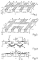
- Figure 1 partially and very schematically shows a portion of a conventional bipolar integrated circuit in perspective view and in section.
- This circuit is developed on a P-type substrate 1 on which is formed an N-type epitaxial layer divided into boxes by isolation walls 2 of P + type. Inside each of the boxes is formed a particular component, for example an NPN or PNP transistor, which is isolated from its neighbors by the isolation walls 2.
- a particular component for example an NPN or PNP transistor, which is isolated from its neighbors by the isolation walls 2.
- the polarity between the wells and the substrate linked to the supply voltage should be such that the NP junction between each well and the substrate is blocked.
- the substrate must be more negatively polarized than each of the wells.
- FIG. 2 In the prior art, in an attempt to resolve this problem of contamination of neighboring caissons of a caisson possibly subjected to different negative voltages, the structure schematically shown in Figures 2 and 3 has been adopted.
- an annular box 6 Around the caisson 3 capable of receiving voltages parasitic negative, an annular box 6 is provided which at least partially surrounds the box 3, and is interposed between the box 3 and the boxes 4 which it is desired to protect.
- a metallization 7 is deposited on the annular well 6, with the interposition, as is usual, of a layer 8 with a high doping level and of the same type of conductivity as that of the well 6 making it possible to ensure the ohmicity of the contact.
- This annular metallization 7 is connected to the positive supply terminal of the integrated circuit.
- an object of the present invention is to provide a new type of device for protection against leakage currents in an integrated circuit having better results than the means employed in the prior art.
- an object of the present invention is to provide such a protection device which does not cause power dissipation in the integrated circuit.
- Another object of the present invention is to provide a protection device reducing the leakage currents by a factor of 10 5 to 10 7 and not simply by 10 like the means of the prior art.
- the present invention provides, as was already known, to surround a box capable of being parasitized by an annular box.
- this annular box is connected to its corresponding external isolation wall.
- the isolation wall separating the parasitic box from the annular box is connected to the most negative potential of the supply voltage.
- the annular box no longer has the same function as that of the prior art and the protection of neighboring caissons of the caisson likely to be parasitized is ensured by the creation of an electric field opposing the diffusion of the electrons generated in the vicinity of the junction between the parasitized caisson and the substrate.
- Figure 4 shows a sectional view of a structure according to the present invention.
- This sectional view corresponds to the top view of FIG. 2, that is to say that the box 3, capable of receiving negative parasitic voltages, is surrounded by an annular box 6 to protect the neighboring boxes 4.
- the difference between the present invention as shown schematically in Figure 4 and the devices of the prior art as shown schematically in Figure 3 lies mainly in the metallizations and connections of the various layers.
- the isolation wall 20 separating the box 3 from the annular box 6 is covered with a metallization 21 connected to the most negative supply terminal of the circuit.
- An overdoped zone 22 of type P + is provided if necessary to improve the ohmicity of the contact between the metallization 21 and the surface of the insulation wall 20.
- the wall d is designated by the reference 30 insulation external to the annular box 6, the apparent surface of this isolation wall is connected by a metallization 31 to the apparent surface of the annular box 6.
- an overdoped layer 8 ensures the ohmicity of the contact between the box 6 and the metallization 31.
- an overdoped area 32 ensures, if necessary, the consistency of the contact between the metallization 31 and the surface of the insulation wall 30.
- Figure 5 substantially repeats Figure 4, but there is shown in addition the circulation of current lines and electric field so that this figure can serve as a support for the following theoretical presentation of the operation of the structure according to the present invention. This theoretical presentation is given only for explanatory purposes to help the reader better understand and generalize the present invention. However, any error or omission in this theoretical description cannot affect the validity of the present invention, the results of which have been observed experimentally by the applicant as will be explained below.
- the conduction current in the substrate resulting from majority carriers (holes) is shown in solid lines, and in dotted lines, the diffusion current of minority carriers (electrons), it being understood that the electrons propagate in the direction inverse of the direction designated by the arrows in the figure which corresponds to the conventional representation of current flow.
- the most negative potential of the power source has been represented by the conventional symbol of the mass.
- the current 41 results from current 40 and is substantially proportional to this current 40 or stray current.
- This current 41 generates in the substrate 1, which has a given resistivity, a radial electric field E oriented towards the outside of the box 3 and also having an intensity roughly proportional to the stray current 40 from which it results.
- the recombination current (not represented in FIG. 5) is supplied to the substrate by the metallization 21 and the wall 20.
- the parasitic current generating electrons in the substrate creates an electric field serving for the confinement of these electrons and produces its own remedy. A correction proportional to the magnitude of the current resulting from the parasitic voltages is thus obtained.
- the quality of this compensation will be illustrated in relation to the diagrams in Figures 6 and 7 below.
- the ordinates indicate the sum of the leakage currents I f in the caissons to be protected such as the caissons 4 of FIG. 2 while the abscissae indicate the parasitic current Ip injected into the parasitic well such as well 3 of FIG. 2.
- the abscissae are in mA and correspond to a variation of the current Ip from 0 to 50 mA and the ordinates are, for FIG. 6 in mA and extend in the range of 0 to 1 mA and for Figure 7 in ltA and extend in the range of 0 to 50, uA
- the curve 50 corresponds to the structures of the prior art as illustrated in FIG. 3 and the curve 51 corresponds to a structure according to the present invention as illustrated in FIGS. 4 and 5.
- FIG. 6 clearly shows that , for a structure according to the prior art, a leakage current of the order of mA is reached for all the transistors to be protected as soon as the injected current reaches a value of the order of 10 mA, that is to say that is to say that only 9/10 of the injected current is absorbed by the annular box.
- the structure according to the present invention makes it possible to obtain leakage currents in the wells 4 to be protected less than a few tens of ⁇ A in a range going from 0 to 30 mA for the injected current, this sum of the leakage currents being even less than the iiA for values of the injected current comprised between approximately 10 and 30 mA.
- Curve 51 is shown in FIG. 7 with a dilated scale on the ordinate.
- the metallization 31 (see FIG. 4) to a metallization integral with the substrate 1 and more particularly with the underside of this substrate.
- the curve 51 is then extended by the dotted curve designated by the reference 52 in FIG. 7 and the device retains all its effectiveness against injected currents which may be greater than 100 mA.
- the present invention has been explained previously in the case of a monolithic integrated circuit produced on a P-type substrate. If the bipolar integrated circuit was produced on an N-type substrate, all that has been said previously would remain valid by inverting all the types of conductivity as well as the directions of the currents. In particular, the reference voltage of the power source which was the most negative voltage in the example described above would be the most positive voltage.
- the metallizations 21 and 31 can be interrupted over a portion of their perimeter to allow passage to other connection metallizations directed towards the component included in the box 3, which avoids having to resort to metallization overlays.
- the isolation walls surrounding the boxes containing these components will be connected to the wall 30 and to the box 6 by appropriately extending the metallization 31; this results in further improved protection of these boxes.
- the present invention may be applied to all integrated circuits which, by their environment, are capable of receiving large parasitic overvoltages, in particular in industrial and automotive electronics.
Landscapes
- Engineering & Computer Science (AREA)
- Physics & Mathematics (AREA)
- Condensed Matter Physics & Semiconductors (AREA)
- General Physics & Mathematics (AREA)
- Manufacturing & Machinery (AREA)
- Computer Hardware Design (AREA)
- Microelectronics & Electronic Packaging (AREA)
- Power Engineering (AREA)
- Semiconductor Integrated Circuits (AREA)
- Bipolar Integrated Circuits (AREA)
Applications Claiming Priority (2)
| Application Number | Priority Date | Filing Date | Title |
|---|---|---|---|
| FR8010842A FR2492165A1 (fr) | 1980-05-14 | 1980-05-14 | Dispositif de protection contre les courants de fuite dans des circuits integres |
| FR8010842 | 1980-05-14 |
Publications (2)
| Publication Number | Publication Date |
|---|---|
| EP0040125A1 EP0040125A1 (fr) | 1981-11-18 |
| EP0040125B1 true EP0040125B1 (fr) | 1983-11-30 |
Family
ID=9241989
Family Applications (1)
| Application Number | Title | Priority Date | Filing Date |
|---|---|---|---|
| EP81400665A Expired EP0040125B1 (fr) | 1980-05-14 | 1981-04-28 | Dispositif de protection contre les courants de fuite dans des circuits intégrés |
Country Status (4)
| Country | Link |
|---|---|
| US (1) | US4466011A (enExample) |
| EP (1) | EP0040125B1 (enExample) |
| DE (1) | DE3161536D1 (enExample) |
| FR (1) | FR2492165A1 (enExample) |
Families Citing this family (28)
| Publication number | Priority date | Publication date | Assignee | Title |
|---|---|---|---|---|
| EP0109996B1 (fr) * | 1982-11-26 | 1987-06-03 | International Business Machines Corporation | Structure de résistance autopolarisée et application à la réalisation de circuits d'interface |
| IT1231894B (it) * | 1987-10-15 | 1992-01-15 | Sgs Microelettronica Spa | Dispositivo integrato per schermare l'iniezione di cariche nel substrato. |
| IT1232930B (it) * | 1987-10-30 | 1992-03-10 | Sgs Microelettronica Spa | Struttura integrata a componenti attivi e passivi inclusi in sacche di isolamento operante a tensione maggiore della tensione di rottura tra ciascun componente e la sacca che lo contiene |
| FR2624320B1 (fr) * | 1987-12-02 | 1990-05-18 | Equip Electr Moteur | Regulateur monolithique de tension de charge de batterie par un alternateur protege contre les tensions parasites |
| DE3924278A1 (de) * | 1988-08-10 | 1990-02-15 | Bosch Gmbh Robert | Elektronisches, monolithisch integriertes geraet |
| IT1231541B (it) * | 1989-07-25 | 1991-12-17 | Sgs Thomson Microelectronics | Dispositivo di protezione contro gli effetti parassiti provocati da impulsi negativi di tensione di alimentazione in circuiti integrati monolitici includenti un dispositivo di potenza per il pilotaggio di un carico induttivo ed un dispositivo di controllo per detto dispositivo di potenza. |
| IT1236797B (it) * | 1989-11-17 | 1993-04-02 | St Microelectronics Srl | Dispositivo monolitico di potenza a semiconduttore di tipo verticale con una protezione contro le correnti parassite. |
| JPH03203265A (ja) * | 1989-12-28 | 1991-09-04 | Sony Corp | 半導体装置 |
| WO1991016728A1 (fr) * | 1990-04-13 | 1991-10-31 | Kabushiki Kaisha Toshiba | Structure de substrat pour un dispositif a semiconducteurs |
| US5148099A (en) * | 1991-04-01 | 1992-09-15 | Motorola, Inc. | Radiation hardened bandgap reference voltage generator and method |
| DE4133245C2 (de) * | 1991-10-08 | 2001-09-20 | Bosch Gmbh Robert | Bipolare monolithisch integrierte Schaltung |
| DE4209523C1 (enExample) * | 1992-03-24 | 1993-03-11 | Siemens Ag, 8000 Muenchen, De | |
| US5243214A (en) * | 1992-04-14 | 1993-09-07 | North American Philips Corp. | Power integrated circuit with latch-up prevention |
| JP3252569B2 (ja) * | 1993-11-09 | 2002-02-04 | 株式会社デンソー | 絶縁分離基板及びそれを用いた半導体装置及びその製造方法 |
| US5514901A (en) * | 1994-05-17 | 1996-05-07 | Allegro Microsystems, Inc. | Epitaxial island with adjacent asymmetrical structure to reduce collection of injected current from the island into other islands |
| US5545917A (en) * | 1994-05-17 | 1996-08-13 | Allegro Microsystems, Inc. | Separate protective transistor |
| US5834826A (en) * | 1997-05-08 | 1998-11-10 | Stmicroelectronics, Inc. | Protection against adverse parasitic effects in junction-isolated integrated circuits |
| WO2003005449A1 (en) * | 2001-07-03 | 2003-01-16 | Tripath Technology, Inc. | Substrate connection in an integrated power circuit |
| JP2003229502A (ja) * | 2002-02-01 | 2003-08-15 | Mitsubishi Electric Corp | 半導体装置 |
| US20040053439A1 (en) * | 2002-09-17 | 2004-03-18 | Infineon Technologies North America Corp. | Method for producing low-resistance ohmic contacts between substrates and wells in CMOS integrated circuits |
| US6747294B1 (en) | 2002-09-25 | 2004-06-08 | Polarfab Llc | Guard ring structure for reducing crosstalk and latch-up in integrated circuits |
| DE10314151B4 (de) * | 2003-03-28 | 2008-04-24 | Infineon Technologies Ag | Halbleiterbauelementeanordnung und Verfahren zur Kompensation parasitärer Ströme |
| CA2533225C (en) | 2006-01-19 | 2016-03-22 | Technologies Ltrim Inc. | A tunable semiconductor component provided with a current barrier |
| US7538396B2 (en) * | 2007-01-19 | 2009-05-26 | Episil Technologies Inc. | Semiconductor device and complementary metal-oxide-semiconductor field effect transistor |
| US7411271B1 (en) * | 2007-01-19 | 2008-08-12 | Episil Technologies Inc. | Complementary metal-oxide-semiconductor field effect transistor |
| US7514754B2 (en) * | 2007-01-19 | 2009-04-07 | Episil Technologies Inc. | Complementary metal-oxide-semiconductor transistor for avoiding a latch-up problem |
| US7700405B2 (en) * | 2007-02-28 | 2010-04-20 | Freescale Semiconductor, Inc. | Microelectronic assembly with improved isolation voltage performance and a method for forming the same |
| US9478607B2 (en) | 2014-09-11 | 2016-10-25 | Semiconductor Components Industries, Llc | Electronic device including an isolation structure |
Citations (4)
| Publication number | Priority date | Publication date | Assignee | Title |
|---|---|---|---|---|
| FR1510057A (fr) | 1966-12-06 | 1968-01-19 | Csf | Transistors intégrés complémentaires npn et pnp à collecteurs isolés |
| CH506889A (de) | 1970-07-24 | 1971-04-30 | Foerderung Forschung Gmbh | Integrierter Schaltkreis |
| FR2113906A1 (enExample) | 1970-11-12 | 1972-06-30 | Itt | |
| FR2303382A1 (fr) | 1975-03-07 | 1976-10-01 | Nat Semiconductor Corp | Circuit integre a region epitaxiale intermediaire separant des regions epitaxiales d'entree et de sortie |
Family Cites Families (7)
| Publication number | Priority date | Publication date | Assignee | Title |
|---|---|---|---|---|
| US4044373A (en) * | 1967-11-13 | 1977-08-23 | Hitachi, Ltd. | IGFET with gate protection diode and antiparasitic isolation means |
| NL161923C (nl) * | 1969-04-18 | 1980-03-17 | Philips Nv | Halfgeleiderinrichting. |
| US3590345A (en) * | 1969-06-25 | 1971-06-29 | Westinghouse Electric Corp | Double wall pn junction isolation for monolithic integrated circuit components |
| US3878551A (en) * | 1971-11-30 | 1975-04-15 | Texas Instruments Inc | Semiconductor integrated circuits having improved electrical isolation characteristics |
| US3931634A (en) * | 1973-06-14 | 1976-01-06 | Rca Corporation | Junction-isolated monolithic integrated circuit device with means for preventing parasitic transistor action |
| US3940785A (en) * | 1974-05-06 | 1976-02-24 | Sprague Electric Company | Semiconductor I.C. with protection against reversed power supply |
| US4027325A (en) * | 1975-01-30 | 1977-05-31 | Sprague Electric Company | Integrated full wave diode bridge rectifier |
-
1980
- 1980-05-14 FR FR8010842A patent/FR2492165A1/fr active Granted
-
1981
- 1981-04-28 EP EP81400665A patent/EP0040125B1/fr not_active Expired
- 1981-04-28 DE DE8181400665T patent/DE3161536D1/de not_active Expired
- 1981-05-13 US US06/263,203 patent/US4466011A/en not_active Expired - Lifetime
Patent Citations (4)
| Publication number | Priority date | Publication date | Assignee | Title |
|---|---|---|---|---|
| FR1510057A (fr) | 1966-12-06 | 1968-01-19 | Csf | Transistors intégrés complémentaires npn et pnp à collecteurs isolés |
| CH506889A (de) | 1970-07-24 | 1971-04-30 | Foerderung Forschung Gmbh | Integrierter Schaltkreis |
| FR2113906A1 (enExample) | 1970-11-12 | 1972-06-30 | Itt | |
| FR2303382A1 (fr) | 1975-03-07 | 1976-10-01 | Nat Semiconductor Corp | Circuit integre a region epitaxiale intermediaire separant des regions epitaxiales d'entree et de sortie |
Also Published As
| Publication number | Publication date |
|---|---|
| EP0040125A1 (fr) | 1981-11-18 |
| US4466011A (en) | 1984-08-14 |
| DE3161536D1 (en) | 1984-01-05 |
| FR2492165B1 (enExample) | 1984-05-04 |
| FR2492165A1 (fr) | 1982-04-16 |
Similar Documents
| Publication | Publication Date | Title |
|---|---|---|
| EP0040125B1 (fr) | Dispositif de protection contre les courants de fuite dans des circuits intégrés | |
| EP0357528B1 (fr) | Transistor MOS composite et application à une diode roue libre | |
| EP0721218B1 (fr) | Circuit intégré de puissance | |
| FR2812972A1 (fr) | Dispositif a semiconducteur consistant en un thyristor pour la protection contre les decharges electrostatiques | |
| FR2503456A1 (fr) | Dispositif de protection pour circuits integres | |
| EP0576375A1 (fr) | Structure de diodes de protection de plot | |
| FR2773265A1 (fr) | Circuit de protection d'interface d'abonnes | |
| FR2550013A1 (fr) | Dispositif pour supprimer les surtensions a semi-conducteurs, dont la tension d'amorcage peut etre predeterminee avec precision, et son procede de fabrication | |
| FR3091024A1 (fr) | Photodiode à avalanche à photon unique | |
| EP0614232B1 (fr) | Diode de référence dans un circuit intégré bipolaire | |
| EP0543745B1 (fr) | Transistor MOS à zener de protection intégrée | |
| FR2739224A1 (fr) | Structure de thyristor commande par resistance de base presentant une implantation haute densite pour une capacite de courant augmentee | |
| EP3276662B1 (fr) | Structure de protection d'un circuit intégré contre les décharges électrostatiques | |
| EP0521802B1 (fr) | Diode à avalanche dans un circuit intégré bipolaire | |
| EP0090686B1 (fr) | Transistor PNP fort courant faisant partie d'un circuit intégré monolithique | |
| EP1076365A1 (fr) | Commutateur statique bidirectionnel sensible | |
| FR2503933A1 (fr) | Circuit integre comprenant un reseau de transistors | |
| WO2002050916A1 (fr) | Commutateur statique bidirectionnel sensible | |
| EP0881672A1 (fr) | Mur d'isolement entre composants de puissance | |
| EP0886316A1 (fr) | Protection du caisson logique d'un composant incluant un transistor MOS de puissance intégré | |
| FR2982077A1 (fr) | Triac a amplification de gachette | |
| FR2693035A1 (fr) | Diode de protection pour composant semiconducteur vertical. | |
| EP0462029A1 (fr) | Procédé de fabrication d'un transistor bipolaire supportant des polarisations inverses | |
| FR2495378A1 (fr) | Circuit de protection, contre les tensions transitoires, comprenant un thyristor (scr), pour circuits integres | |
| EP0987751A1 (fr) | Mur d'isolement entre composants de puissance |
Legal Events
| Date | Code | Title | Description |
|---|---|---|---|
| PUAI | Public reference made under article 153(3) epc to a published international application that has entered the european phase |
Free format text: ORIGINAL CODE: 0009012 |
|
| AK | Designated contracting states |
Designated state(s): DE FR GB IT NL |
|
| 17P | Request for examination filed |
Effective date: 19811128 |
|
| ITF | It: translation for a ep patent filed | ||
| GRAA | (expected) grant |
Free format text: ORIGINAL CODE: 0009210 |
|
| AK | Designated contracting states |
Designated state(s): DE FR GB IT NL |
|
| REF | Corresponds to: |
Ref document number: 3161536 Country of ref document: DE Date of ref document: 19840105 |
|
| PLBI | Opposition filed |
Free format text: ORIGINAL CODE: 0009260 |
|
| 26 | Opposition filed |
Opponent name: DEUTSCHE ITT INDUSTRIES GMBH Effective date: 19840809 |
|
| PLBN | Opposition rejected |
Free format text: ORIGINAL CODE: 0009273 |
|
| STAA | Information on the status of an ep patent application or granted ep patent |
Free format text: STATUS: OPPOSITION REJECTED |
|
| 27O | Opposition rejected |
Effective date: 19851011 |
|
| NLR2 | Nl: decision of opposition | ||
| PGFP | Annual fee paid to national office [announced via postgrant information from national office to epo] |
Ref country code: NL Payment date: 19900430 Year of fee payment: 10 |
|
| ITTA | It: last paid annual fee | ||
| PG25 | Lapsed in a contracting state [announced via postgrant information from national office to epo] |
Ref country code: NL Effective date: 19911101 |
|
| NLV4 | Nl: lapsed or anulled due to non-payment of the annual fee | ||
| REG | Reference to a national code |
Ref country code: FR Ref legal event code: D6 |
|
| PGFP | Annual fee paid to national office [announced via postgrant information from national office to epo] |
Ref country code: FR Payment date: 20000411 Year of fee payment: 20 |
|
| PGFP | Annual fee paid to national office [announced via postgrant information from national office to epo] |
Ref country code: GB Payment date: 20000426 Year of fee payment: 20 |
|
| PGFP | Annual fee paid to national office [announced via postgrant information from national office to epo] |
Ref country code: DE Payment date: 20000427 Year of fee payment: 20 |
|
| PG25 | Lapsed in a contracting state [announced via postgrant information from national office to epo] |
Ref country code: GB Free format text: LAPSE BECAUSE OF EXPIRATION OF PROTECTION Effective date: 20010427 |
|
| REG | Reference to a national code |
Ref country code: GB Ref legal event code: PE20 Effective date: 20010427 |