EP0033469B1 - Verfahren und Schaltungsanordnung zum Übertragen von binären Signalen zwischen Anschlussgeräten - Google Patents
Verfahren und Schaltungsanordnung zum Übertragen von binären Signalen zwischen Anschlussgeräten Download PDFInfo
- Publication number
- EP0033469B1 EP0033469B1 EP81100393A EP81100393A EP0033469B1 EP 0033469 B1 EP0033469 B1 EP 0033469B1 EP 81100393 A EP81100393 A EP 81100393A EP 81100393 A EP81100393 A EP 81100393A EP 0033469 B1 EP0033469 B1 EP 0033469B1
- Authority
- EP
- European Patent Office
- Prior art keywords
- signal
- pdn
- bus line
- signals
- peripheral device
- Prior art date
- Legal status (The legal status is an assumption and is not a legal conclusion. Google has not performed a legal analysis and makes no representation as to the accuracy of the status listed.)
- Expired
Links
Images


Classifications
-
- G—PHYSICS
- G06—COMPUTING OR CALCULATING; COUNTING
- G06F—ELECTRIC DIGITAL DATA PROCESSING
- G06F13/00—Interconnection of, or transfer of information or other signals between, memories, input/output devices or central processing units
- G06F13/14—Handling requests for interconnection or transfer
- G06F13/20—Handling requests for interconnection or transfer for access to input/output bus
- G06F13/22—Handling requests for interconnection or transfer for access to input/output bus using successive scanning, e.g. polling
-
- G—PHYSICS
- G06—COMPUTING OR CALCULATING; COUNTING
- G06F—ELECTRIC DIGITAL DATA PROCESSING
- G06F13/00—Interconnection of, or transfer of information or other signals between, memories, input/output devices or central processing units
- G06F13/14—Handling requests for interconnection or transfer
- G06F13/20—Handling requests for interconnection or transfer for access to input/output bus
- G06F13/28—Handling requests for interconnection or transfer for access to input/output bus using burst mode transfer, e.g. direct memory access DMA, cycle steal
- G06F13/285—Halt processor DMA
Definitions
- the invention relates to a method and a circuit arrangement for transmitting binary signals between connection devices connected at least to signal transmitters and connection devices connected at least to signal receivers, all connection devices being connected to one another via a central bus line system and to a central control device controlling the signal transmission between them , which comprises at least one central processor, in particular a microprocessor, with associated program and working memories, and wherein with the help of the central processor, addresses identifying the individual connection devices can be generated in succession.
- control station provided there addresses the individual subscriber transmission stations in a scanning process in order to then send out messages to be sent out together with the address designating the desired recipient.
- control station is exposed to a considerable load.
- a message transmission system is now also known (US Pat. No. 4,174,536) which has a microprocessor which is connected to memories and to serial and parallel interfaces via an address bus line and via a data bus line.
- the microprocessor is thus constantly involved in the connection to the bus lines and thus to the devices connected to them.
- a data connection system is already known (DE-A 1 - 2 831 887), in which a plurality of so-called subsystems are connected to one another.
- Such a subsystem contains a microprocessor, which is connected via a bus line system to a memory arrangement and to input / output modules. With this circuit structure too, the microprocessor is always involved in the connection with the individual devices connected to the bus line system.
- the invention is based on the object of showing a way in which, in a method and a circuit arrangement of the type mentioned at the outset, binary signals of practically any number can be transmitted between connecting devices connected to one another via a central bus line system, without the need for different sequence procedures in the form of separate command sequences must be provided, according to which the respective signal transmission is handled.
- the invention has the advantage that it is possible to do without the provision of separate sequence procedures in order to transmit binary signals of different numbers from one connection device to another connection device, without having to include a separate buffer arrangement in this transmission.
- the signals in question are advantageously transmitted in the form of signal groups or bytes or byte groups, the extent of such signal groups or bytes or byte groups being known to the memory access device from the occurrence of a transmitted signal transmission request signal.
- this memory access device it is then possible in a relatively simple manner to determine, on the basis of the request signal indicating the scope of the signal transmission, the number of control signals which are to be supplied to the connection devices involved in the respective transmission for controlling the signal delivery or the signal reception.
- the measures according to the invention result in a relatively strong relief for the central processor used.
- a circuit arrangement is preferably used to carry out the method according to the invention, in which all connection devices are connected to a central bus line system to which a central control device is connected, which comprises at least one central processor, in particular a microprocessor, with associated program and working memories.
- this circuit arrangement is characterized by the features specified in claim 4. It has the advantage of a low overall circuit complexity in the individual connection devices and thus in the entire transmission system.
- circuit arrangement considered above is designed in the manner specified in claim 5, there is the advantage of a particularly low outlay in terms of circuitry in the respective connection device.
- circuit arrangement considered above is configured in the manner characterized in claim 7, the advantage of a particularly low circuit complexity for the connection of the signal transmitters or signal receivers of the individual connection devices is achieved.
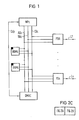
- a circuit arrangement is shown in a block diagram, which is used for the transmission of binary signals between connecting devices PD1 to PDn.
- These connection devices PD 1 to PDn are connected to one another via a central bus line system.
- This central bus line system includes an address bus line ABc, a data bus line DBc and a control bus line CBc.
- Each of these three bus lines normally has a plurality of individual lines, for example eight or sixteen lines.
- the connection device PD1 is also connected to a transmission line L, which may lead to at least one signal transmitter and / or at least one signal receiver.
- the connection device PDn is also connected to a transmission line Ln, which may lead to at least one signal receiver and / or at least one signal transmitter.
- a central control device which controls the signal transmission between the connection devices PD1 to PDn and which comprises at least one central processor MPc and one memory access device DMAC serving for direct memory access is connected to the central bus line system.
- the central processor MPc is formed in particular by a microprocessor.
- the relevant central processor MPc is additionally connected to the memory access device DMAC via a separate control line Cdp. Via this control line, the central processor MPc can be ineffectively controlled from the memory access device DMAC with regard to the delivery of signals to the central bus line system. This is usually done by controlling the relevant connections of the central processor MPc in the high-resistance state.
- the central control device also includes a program memory ROMc and a working memory RAMc.
- the program memory ROMc is a read memory, which can also be programmable if necessary.
- the RAMc is a random access memory.
- the program memory ROMc and the main memory RAMc are connected to the bus lines ABc, DBc, CBc of the central bus line system with corresponding connections.
- connection devices PD1 to PDn shown in FIGS. 2A and 2B are to be placed side by side in the manner shown in FIG. 2C.
- the connection device shown in detail in FIGS. 2A and 2B has an internal control device which, according to FIG. 2A, is formed by a microprocessor MPp.
- This microprocessor MPp is connected with addressing, data and control connections to bus lines belonging to an internal bus line system.
- These bus lines include an internal address bus line ABp, an internal data bus line DBp and an internal control bus line CBp.
- These bus lines also each comprise a plurality of lines.
- the bus lines ABp, DBp, CBp of the internal bus line system are connected to the bus lines ABc, DBc and CBc of the central bus line system via release circuits which are considered in more detail below.
- the internal address bus line ABp is connected to the central address bus line ABc via an address enable circuit ADF.
- This address enable circuit ADF can contain a number of AND gates G11 to G 1 n, which allow address transmission only from the central address bus line ABc to the internal address bus line ABp. In any case, an address transfer in the opposite direction is not possible via the address enable circuit ADF and is also not intended.
- the release of the address transmission in the address release circuit ADF takes place in that the relevant address release circuit ADF is supplied with a binary signal "1" via an enable line FRG As can be seen from FIG. 2A, the line FRG is connected to the output of a NAND gate G 16.
- the internal data bus line DBp is connected to the central data bus line DBc via a data switch DATW which, depending on its setting, enables data transmission either from the central data bus line DBc to the internal data bus line DBp or from the internal data bus line DBp to the central data bus line DBc.
- the data switch DATW contains a number of pairs of AND gates G21, G22 to G2x, G2y which fulfill switch functions and are each controlled by an AND gate of two AND gates G3, G4.
- the AND gate G4 receives the signals fed to its input in inverted form, so that it actually fulfills the function of a blocking element.
- the two AND gates G3 and G4 are connected in parallel on the input side, it is thus ensured that only one of these two AND gate outputs outputs a binary signal 1 "on a corresponding control.
- the two AND- Gates G3, G4 are connected in common to the output of the previously mentioned NAND gate G16.
- the other inputs connect the two AND gates G3, G4 to the output of a control bus enable circuit CBF.
- the AND gates G21, G22 to G2x, G2y are like the AND gates G11 to G1n formed by so-called tristate logic gates, which have a high-impedance output when there is no control.
- the control bus enable circuit CBF connects some control lines of the central control bus line CBc to some of the control lines of the internal control bus line CBp.
- the input lines connected to the central control bus line CBc are designated MEMR, IOR and MEMW.
- the output lines leading to the internal control bus line CBp are designated with MEMRI or MEMWI.
- the control bus enable circuit CBF contains three AND gates G5, G6, G8, which are connected with their one inputs to the lines MEMR, IOR and MEMW. With their other inputs, the relevant AND gates G5, G6 and G8 are connected to lines RDST and RDBF and WREX, respectively, which lead to a logic circuit arrangement HLDS of the arrangement shown in FIG. 2A.
- the outputs of the two AND gates G5 and G6 are connected to the inputs of an OR gate G7.
- the control line already mentioned is connected to the output of the OR gate G7 and leads from the control bus enable circuit CBF to the data switch DATW.
- the output line MEMRI already mentioned is connected to the output of the OR gate G7 via an isolating amplifier TA.
- the other output line MEMWI already mentioned is connected to the output of the AND gate G8. This line leads to an input of the NAND gate G18.
- the internal control device of the connection device shown as an exemplary embodiment in FIGS. 2A and 2B now not only includes the microprocessor MPp shown in FIG. 2A, but also a program memory ROMp and a working or data memory RAMp also belong to this internal control device. These two memories ROMp, RAMp are each connected via a separate access control circuit ZST2 or ZST3 with corresponding connections to all bus lines of the internal bus line system.
- an interface circuit USART is connected to the internal bus line system via an associated access control circuit ZST1.
- this interface circuit USART is connected to a transmission line L to which at least one signal transmitter or a signal receiver can be connected, which is provided for the delivery or reception of binary signals.
- the relevant signal transmitter or Signal receivers may in particular be a teleprinter or a synchronous data connection.
- a plurality of signal transmitters / signal receivers can be connected to the internal bus line system via a corresponding number of interface circuits.
- the microprocessor MPp belonging to the internal control device of the connection device according to FIGS. 2A and 2B is connected with a hold signal input HLD and with a hold signal output HLDA to a hold signal transmission circuit HLDA, which in the present case may contain two switch circuits or multiplexer circuits MUX1, MUX2 .
- These multiplexer circuits MUX1, MUX2 are controlled by a control signal which can be supplied to a control input E (binary signal "0" or binary signal "1") in such a way that they connect the relevant connections HLD, HLDA of the microprocessor MPp either with the lines HLDE, HLDAE or with the lines HLDAIi , HLDAi connect.
- a memory access device DMA module
- DMA module can be connected to the last-mentioned lines, for example.
- the two lines HLDE and HLDAE connect the hold signal transmission circuit HLDA with the above-mentioned logic circuit arrangement HLDS.
- the line HLDE is connected to the output of an OR gate G 10 belonging to the logic circuit arrangement HLDS.
- the line HLDAE is connected to the one inputs of AND gates G13, G14, G15, G16, G17 and G27 of the logic circuit arrangement HLDS.
- the last-mentioned AND gates G13 to G17 of the logic circuit arrangement HLDS are connected on the output side to the lines RDBF, WREX, RDST, FRG and WRCM designated in FIG. 2A.
- the lines WDBF, WREX and RDST lead to corresponding inputs of the control bus enable circuit CBF.
- the line FRG which may be referred to as the enable line, leads to corresponding enable inputs of the address enable circuit ADF and the data switch DATW.
- the line WRCM is connected to the second input of the already mentioned NAND gate G 18.
- the AND gate G 13 of the logic circuit arrangement HLDS is connected with its not yet considered input to an input of the relevant circuit HLSD, to which a line DACT leads, which is connected to an output of an access control device ZUS shown in FIG. 2B. Furthermore, two OR gates G9 and G 12, each with one input, are connected to the input of the logic circuit arrangement HLDS just considered.
- the OR gate G9 is connected with a further input together with an input of an OR gate G11 to an input of the logic circuit arrangement HLDS, to which a line DACR is connected, which is connected to a further output of the access control device ZUS.
- the aforementioned OR gate G9 is connected on the output side to the set input S of a bistable flip-flop FF1.
- the relevant bistable flip-flop FF1 With its reset input R, the relevant bistable flip-flop FF1 is connected to an input of the logic circuit arrangement HLDS, to which a line INTEI is connected, which is connected to the output of a display circuit TRE indicating the end of a signal transmission.
- the bistable flip-flop FF1 With its output Q carrying a binary signal "1" in the set state, the bistable flip-flop FF1 is connected to an input of the OR gate G 10.
- the relevant OR gate G 10 is connected to corresponding inputs of the OR gate G 12 at inputs of the logic circuit arrangement HLDS, to which two lines STAT and CMD are connected, which lead away from an address detector device GAD indicated in FIG. 2B .
- the OR gate G 11 already mentioned is connected with its not yet considered input to the input of the logic circuit arrangement HLDS connected to the line CMD. With its output, the OR gate G11 is connected to a further input of the AND gate G14.
- the second gate of the AND gate G15 is connected to the input of the logic circuit arrangement HLDS connected to the line STAT.
- the AND gate G 16 is connected with its second input to the output of the OR gate G12.
- the second gate of the AND gate G17 is connected directly to the input of the logic circuit arrangement HLDS connected to the line CMD.
- the AND gate G27 is connected to the HLDAE line with an (inverting) input and with another input to the output of the OR gate G12.
- the (inverting) output of the AND gate (tri-state gate) G27 is connected to the control bus line CBc via a line NRDY.
- the access control device ZUS shown in FIG. 2B has a bistable flip-flop FF3 used as a transmission flip-flop and a bistable flip-flop FF4 used as a reception flip-flop.
- the flip-flop FF3 is connected with its set input S to an output line DEL2 of a decoder Dec2; the flip-flop FF4 is connected with its set input S to an output line DEL1 of this decoder Dec2.
- the decoder Dec2 is connected on the input side to the internal address bus line ABp and also to at least one control line of the internal control bus line CBp.
- the decoder Dec2 which can only output a binary output signal "1" at one of its outputs, is connected to the DEL3, DEL4 and DEL5 lines with further outputs.
- the line DEL3 leads to an input of a transfer end control device RRS, which is indicated in the lower part of FIG. 2B.
- a bistable flip-flop FF7 is connected with its set input S to the relevant line DEL3.
- the line DEL4 leads to an input of the display circuit TRE already mentioned; the reset inputs R of two bistable flip-flops FF5 and FF6 may be connected to this input.
- the line DEL5 leads to the reset input R of the bistable flip-flop FF2 indicated in FIG. 2A.
- This bistable flip-flop is connected with its output Q, which carries a binary signal "1" in the set state, to an interrupt input INTC of the microprocessor MPp.
- the INTEI line is connected to a further interrupt input of the microprocessor MPp.
- An input of the access control device ZUS mentioned above is also connected to the last-mentioned line INTEI.
- the reset inputs R of the two bistable flip-flops FF3 and FF4 may be connected to this input.
- the bistable flip-flop FF3 is connected with its Q output to an input of an AND gate G 19.
- the bistable flip-flop FF3 is connected with its Q output via a request signal line REQ to the central control bus line CBc.
- a further input of the access control device ZUS is connected to a line of the central control bus line CBc via an access control line DAC.
- a further input of the AND gate G 19 and an input of an AND gate G20 are connected to this input of the access control device ZUS. This AND gate G20 is connected to a further input at the Q output of the bistable flip-flop FF4.
- the outputs of the two AND gates G 19, G20 are connected to the lines DACT and DACR already mentioned above.
- the relevant outputs of the two AND gates G19, G20 are connected to the inputs of an OR gate G21 belonging to the display circuit TRE.
- this OR gate G21 is connected to a (negating) input of an AND gate G22 which fulfills a blocking element function and to an input of an AND gate G23.
- the AND gate G23 is connected to a further input with a line TC which is connected to a line of the central control bus line CBc.
- the output of the AND gate G23 is connected to the set input S of the bistable flip-flop FF6.
- the Q output of the bistable flip-flop FF6 is connected to the second input of the AND gate G22, which is connected on the output side to the set input S of the bistable flip-flop FF5.
- the Q output of the bistable flip-flop FF5 is connected to the line INTEI already mentioned above.
- the address detector device GAD shown in more detail in FIG. 2B contains a comparator VGL which is connected with its one input side to the address bus line ABc of the central bus line system and with its other input side is connected to the output of a word memory WM.
- This word memory WM contains an address specific to the connecting device in question, when it occurs on the address bus line ABc, the comparator VGL outputs a binary signal "1" on the output side to release the decoder Dec1, which is also connected on the input side to the address bus line ABc of the central bus line system.
- this decoder Dec1 emits a binary signal "1" to one of its three indicated outputs in accordance with a corresponding decoding of an address supplied to it on the input side.
- the lines STAT and CMD already mentioned above are connected to the relevant outputs of the decoder Dec1.
- a line INZ is connected to an output of the decoder Dec, which line is connected to the one inputs of two AND gates G25, G26 of the transfer end control device RRS according to FIG. 2B.
- These two AND gates G25 and G26 are connected with their other inputs via a line MEMR or via a line MEMW to corresponding control devices of the central control bus line CBc of the central control bus line system.
- the bistable flip-flop FF7 belonging to the aforementioned transfer end control device RRS is connected with its reset input R to the output of the AND gate G26. With its Q output, the bistable flip-flop FF7 is connected to an input of an AND gate G24, which is connected to a further input at the output of the AND gate G25.
- the output of the AND gate G24 which may also be a so-called tri-state gate, is connected via a line D0 to a line of the central data bus line DBc.
- the aforementioned Q output of the bistable flip-flop FF7 is also connected via a negator NG and a line INT to a line of the central control bus line CBc.
- FIGS. 2A and 2B After the possible construction shown in FIGS. 2A and 2B of one of the connection devices provided in the circuit arrangement according to FIG. 1 has been explained above, the mode of operation of the circuit arrangement shown in FIG. 1 is now generally considered. Thereafter, details of this operation will be discussed with reference to Figs. 2A and 2B.
- the transmission of binary signals takes place between the connection devices PD 1 and PDn indicated there, in that first a signal signal is sent from the one connection device, for example the connection device PD1 the central control device is delivered or picked up by the latter.
- This message signal denotes the presence of a signal transmission request from the relevant reporting connection device to at least one other connection device, such as the connection device PDn.
- Such signal signals are stored in the data memory RAMc of the central control device.
- the central processor MPc of this central control device uses such signaling signals to check the individual connection devices that have issued these signaling signals to determine whether signals for signal transmission are already available in these connection devices. This checking process can be a cyclical polling process, through which the above-mentioned message signal can also be picked up by the central control device.
- connection device PD1 Upon determining the presence of a number of signals requiring signal transmission in a connection device, such as connection device PD1, this connection device issues a signal transmission display signal to the central control device upon its corresponding check.
- the connection devices intended for signal recording in the present case the connection device PDn, are supplied with a setting signal which converts this from an initial state into a reception state.
- the connection device PD1 is supplied with a setting signal which converts it from an initial state into a transmission state.
- a control signal is emitted from the connection device PD1 set in the transmission state (via the line REQ), which requests the processing of a signal transmission to the connection devices (PDn) set in the reception state.
- the memory access device DMAC was previously informed by the central processor MPc about the scope of the signal transmission and the address range which is provided for the signal transmission in the connection devices.
- the memory access device DMAC of the central control device issues a control signal which ineffectively controls the central processor MPc with regard to the delivery of signals to the central bus line system. This control signal is transmitted via the control line Cdp.
- the DMAC memory access device now takes over control tasks.
- the memory access device DMAC then outputs separate control signals together with the required addresses in alternating sequence to the relevant connection devices PD1, PDn.
- Two different control signals are emitted; the one control signal is used to control the delivery of binary signals from the connection device PD1 which is in the transmission state, and the other control signal is used to control the reception of these binary signals by the connection devices which are in the reception state, in the present case the connection device PDn.
- the central processor MPc is ineffective during the signal transmission phase; the memory access device DMAC takes on control tasks which relieve the central processor MPc.
- the memory access device DMAC can thus use the address pool of this central processor MPc for the control of the individual connecting devices during the period in which the central processor MPc is ineffectively controlled, in conjunction with a separate control signal which, in connection with the relevant addresses of the central processor MPc does not normally occur. An expansion of the entire address list is thus achieved.
- addresses which are not used by the central processor MPc to be used in the memory access device DMAC for activating the connection devices, in particular for controlling the buffer memories of the connection devices.
- binary signals can be transmitted from one connection device to another connection device via the central bus line system, but binary signals can also be transmitted from one connection device to a large number of further connection devices as part of a signal distribution process via the central bus line system .
- the binary signals emitted by a connecting device can either be delivered simultaneously to all other connecting devices that are possible, or the relevant binary signals can be sequentially supplied to these further connecting devices.
- connection device shown in FIGS. 2A and 2B is in its initial state, which is a ready state for the reception of binary signals representing data. If data occurs in this state on the transmission line L, for example signaling characters which are intended to be stored in the buffer memory BM of the data memory RAMp, the following processes take place.
- the binary signals appearing on the transmission line L are initially picked up by the interface circuit USART.
- the presence of such signals in the interface circuit USART is checked using the internal microprocessor MPp e.g. polled repeatedly. If it is determined in the course of such a query that binary signals have been received by the USART interface circuit, the microprocessor MPp controls the transfer or storage of these signals into the buffer memory BM or into the pre-buffer of the data memory RAMp connected to it.
- the buffer memory BM When such binary signals are successively stored in the buffer memory BM (after buffering, if necessary, in a pre-buffer), information about the scope of the binary signals stored in the buffer memory BM is entered in the associated status pool SP of the data memory RAMp.
- connection device under consideration at least one further connection device.
- buffer memory BM it should also be noted that its address range can be fixed or can be specified by a connection device during the determination of a signal transmission request.
- each buffer memory is expediently divided into a plurality of memory areas in order to be able to store a large number of binary signals. It can then be proceeded in detail such that the control device associated with the connection device in the transmitting state first of all converts the binary signals from the individual pre-storage areas of the associated buffer memory that are suitable for transmission to the buffer memory of at least one connection device in the receiving state, into one defined by a pre-stored area Address designated separate memory area of the relevant buffer memory can be stored.
- a read command signal or a write command signal is issued to the buffer memories of the connection devices involved in a signal transmission.
- the binary signals stored in the separate memory area of the buffer memory of the connection device in the transmission state are then read out and written into a correspondingly addressed memory area of the buffer memory of the connection device in the reception state.
- the binary signals written in the relevant separate memory area of the buffer memory of the respective connection device in the receive state are then under the control of the control device associated with the respective connection device in the receive state (that is the microprocessor MPp) in other memory areas of the relevant buffer memory before being stored by the relevant connection device are delivered.
- the buffer memory of each connection device is optionally used to emit or receive binary signals to at least one or from at least one other corresponding buffer memory.
- This prerequisite is that the central control device according to FIG. 1 already knows which connection devices want to provide binary signals for transmission and to which connection devices these binary signals are to be transmitted.
- Such information will expediently be stored in the RAMc of the central control device.
- This information can be provided by the respective connection device in question, such as the connection device shown in FIGS. 2A and 2B, via the associated data switch DATW.
- the relevant information can represent the addresses that have been read out from the data memory RAMp, for example, under the control of the central microprocessor MPc.
- these addresses therefore represent signal signals - the central processor MPc belonging to the central control device repeatedly asks those connection devices for the presence of signal transmission requests that are recorded as connection devices, from which binary signals are to be transmitted to other connection devices. For this purpose, the central processor MPc cyclically releases the addresses of the relevant connection devices in succession. These addresses appear on the central address bus line ABc. In the case of the connection device shown in FIGS. 2A and 2B, such an address is picked up by the address detector device GAD and compared with the address which designates the connection device in question and which is contained in the word memory WM.
- the intended comparator VGL determines that the addresses compared with one another match, it releases the decoder Dec 1 for the decoding of at least some of the addresses supplied by the central address bus line ABc.
- the decoder Dec1 outputs a binary signal "1" on the STAT line. The occurrence of this binary signal "1" causes a stop signal to be output via the OR gate G10 and the line HLDE to the input HLD of the microprocessor MPp, which then stops performing its operations. If the microprocessor MPp is stopped, it emits an acknowledgment signal indicating this state from the HLDA output in the form of a binary signal "1".
- the AND gate G27 outputs a "0" signal to the central control bus line CBc via the line NRDY.
- This signal signals (the central control device) that the connection device in question is not yet ready for a signal or control signal recording. Such readiness is only given when the "1" signal is present on the HLDAE line.
- This binary signal "1” also reaches the one inputs of the AND gates G13 to G17. In the present case, the two AND gates G 15 and G 16 can be transferred from these AND gates; on the output side, they each emit a binary signal "1.
- the binary signal "1" occurring on the line FRG also has the effect that the AND gates G11 to G 1 of the address enable circuit ADF are controlled so that they can be transmitted.
- Such queries can be carried out over several cycles.
- the microprocessor MPp of the connection device under consideration After the disappearance of the binary signal "1" on the STAT line, the microprocessor MPp of the connection device under consideration returns to its normal state, in which it carries out control tasks in accordance with the program contained in its associated program memory ROMp.
- the central processor MPc recognizes on the basis of the status information that there is a signal transmission request relating to the actual transmission of binary signals between the connection devices already described.
- the central processor MPc then issues a command signal first to the connection devices provided for the reception state and then to the connection device provided for the transmission state.
- the relevant status information provides an indication of the scope of the signal transmission to be carried out, i.e. how many binary signals or bytes or byte groups are to be transmitted.
- connection device In the connection device shown in FIGS. 2A and 2B, the occurrence of the connection device address given as a result of the command signal leads to the associated address detector device GAD issuing a binary signal “1” via the command line CMD.
- the occurrence of this binary signal "1” has the consequence that the associated internal microprocessor MPp is brought back into its hold state and that binary signals "1" then appear on the lines WREX, FRG and WRCM.
- the microprocessor MPp now outputs an address via the internal address bus line ABp, which the decoder Dec2 after emitting a binary signal "1 via the line DEL1 (in the case of connection devices provided for the reception state) or via the line DEL2 (in the case of connection devices intended for the transmission state)
- the occurrence of this binary signal "1" leads to the setting of the receive flip-flop FF4 or the send flip-flop FF3.
- the binary flip-flop FF3 then emits a binary signal "1" as a request signal via the line REQ to the central control device according to FIG.
- the connecting devices to be included in a signal transmission are now in the transmission state or in the reception state.
- the control of the transmission processes now to be carried out takes place under the influence of the memory access device DMAC according to FIG. 1.
- the memory access device DMAC first gives the central processor MPc of the central control device with regard to the delivery of signals to the central one Bus line system ineffective controlling control signal from the control line Cdp.
- the memory access device DMAC successively delivers control signals or control pulses via the line DAC to the central control device.
- the occurrence of these signals in the connection device in the transmission state causes binary signals "1" to be emitted via the line DACT, the occurrence of which signals that the bistable flip-flop FF1 is set and the associated internal microprocessor MPp is thus stopped again.
- binary signals "1" are emitted via the lines RDBF and FRG.
- the data switch DATW of the relevant connection device in conjunction with the binary signal "1" on the line FRG, causes the data switch DATW of the relevant connection device to be set in such a way that data or data can be obtained via it binary signals can be transmitted from the internal data bus line DBp to the central data bus line DBc.
- the relevant binary signals are read out from the buffer memory BM of the relevant connection device. For this purpose, a corresponding address is supplied to the associated data memory RAMp via the address enable circuit ADF which is controlled in the transferable state.
- the occurrence of the control signals or pulses on line DAC leads to a binary signal "1" being output by the associated line DACR.
- the occurrence of this binary signal "1" results in the following processes in the relevant connection device.
- the associated bistable flip-flop FF1 is set, as a result of which the associated internal microprocessor MPp is also brought into the holding state.
- the lines WREX and FRG of the relevant connection device each carry a binary signal "1".
- the memory access device DMAC After the transmission of the last binary signal from the connection device in the transmission state to the connection device (s) in the reception state, the memory access device DMAC according to FIG. 1 emits a separate control signal via the line TC.
- This control signal occurs in the form of a binary signal "0" together with the last binary signal "0" on the associated line DAC.
- the bistable flip-flop FF6 of the associated display circuit TRE is thus set.
- the bistable flip-flop FF5 of the relevant display circuit TRE is then also set. A binary signal "1" is thus emitted via the INTEI line of the relevant connection device.
- this binary signal “1” means that the associated send or receive trigger circuit FF3 or FF4 is switched to the reset state and that the bistable trigger element FF1 is reset. It also causes be Acknowledging binary signal "1" that the microprocessor MPp of the relevant connection device is brought back out of its holding state, in which it was in the course of the relevant signal transmission. The microprocessor MPp can now delete the corresponding setting signals which are stored in the command register CR of its associated data memory RAMp. This means that the relevant connection device is transferred from its send state to its initial state.
- the microprocessor MPp of the connection device under consideration can also give the decoder Dec2 such an address that this decoder Dec2 emits a binary signal “1” via its output line DEL4. This then controls the bistable flip-flops FF5 and FF6 of the associated display device TRE back into the reset state .
- connection device which was in the transmission state is again in its initial state.
- the connection device (s) that were or have been in the receive state emit a signal to the central control device (via the INT line), e.g. after they have processed or forwarded the received binary signals.
- a notification signal is emitted by the transfer end control device RRS indicated in FIG. 2B via the line INT.
- a binary signal "0" is output via the line INT when the bistable flip-flop FF7 of the associated transfer end control device RRS is set.
- This bistable flip-flop FF7 would be set in the course of the above-described transmission termination process in the connection devices which were previously still in the receiving state by the associated decoder Dec2 emitting a binary signal "1 via its output line DEL3. This is the case if the A corresponding address signal from the associated microprocessor MPp is supplied to decoder Dec2. If several connection devices have been received, each of these connection devices emits a binary signal "0" via its line INT.
- the central processor MPc determines which connection device has such a signal has issued by successively addressing the relevant connection devices (delivery of a binary signal "1" via the INZ line) and in each case sending a query signal via the MEMR line to the AND gate G25 and thereby querying the state of the flip-flop FF7 via the AND gate G24 If the associated bistable flip-flop FF7 is set, there is s AND gate G24 via the output line D0 from a binary signal "1", on the reception of which the central processor MPc sends a signal via the line MEMW together with the same address as when querying this state for resetting the flip-flop FF7 via the AND Link G26 delivers.
- the central processor MPc receives knowledge of the termination of the signal transmission through the reception of the binary signals "1" emitted via the INT line; he can then delete the states relating to the signal transmission in the central control area. In addition, he can again handle other signal transmission-related processes. Before doing so, however, the reset operations described must be completed, which relate to the reset of the respective flip-flop FF7.
- the central processor MPc and the microprocessor MPp can be formed by microprocessors of the type 8085 from Intel.
- the memory access device DMAC can be formed by a type 8257 module from Intel.
- the program memories ROMc, ROMp can be formed by type 8708 blocks from Intel.
- the RAMc and the RAMp data memory can be formed by one or more Intel 2119 modules.
- the USART interface circuit can be formed by a module of the type 8251 A from the named company.
- the switch circuits MUX 1, MUX2 can be formed by modules of the type SN74151. Conventional integrated circuits can be used for the other circuit elements indicated in FIGS. 2A and 2B.
Landscapes
- Engineering & Computer Science (AREA)
- Theoretical Computer Science (AREA)
- Physics & Mathematics (AREA)
- General Engineering & Computer Science (AREA)
- General Physics & Mathematics (AREA)
- Communication Control (AREA)
- Multi Processors (AREA)
- Bus Control (AREA)
- Reduction Or Emphasis Of Bandwidth Of Signals (AREA)
- Data Exchanges In Wide-Area Networks (AREA)
Priority Applications (1)
| Application Number | Priority Date | Filing Date | Title |
|---|---|---|---|
| AT81100393T ATE8444T1 (de) | 1980-01-30 | 1981-01-20 | Verfahren und schaltungsanordnung zum uebertragen von binaeren signalen zwischen anschlussgeraeten. |
Applications Claiming Priority (2)
| Application Number | Priority Date | Filing Date | Title |
|---|---|---|---|
| DE3003340 | 1980-01-30 | ||
| DE3003340A DE3003340C2 (de) | 1980-01-30 | 1980-01-30 | Verfahren und Schaltungsanordnung zur Übertragung von binären Signalen zwischen über ein zentrales Busleitungssystem miteinander verbundenen Anschlußgeräten |
Publications (2)
| Publication Number | Publication Date |
|---|---|
| EP0033469A1 EP0033469A1 (de) | 1981-08-12 |
| EP0033469B1 true EP0033469B1 (de) | 1984-07-11 |
Family
ID=6093291
Family Applications (1)
| Application Number | Title | Priority Date | Filing Date |
|---|---|---|---|
| EP81100393A Expired EP0033469B1 (de) | 1980-01-30 | 1981-01-20 | Verfahren und Schaltungsanordnung zum Übertragen von binären Signalen zwischen Anschlussgeräten |
Country Status (6)
| Country | Link |
|---|---|
| US (1) | US4404650A (da) |
| EP (1) | EP0033469B1 (da) |
| AT (1) | ATE8444T1 (da) |
| AU (1) | AU6672681A (da) |
| DE (1) | DE3003340C2 (da) |
| DK (1) | DK40381A (da) |
Families Citing this family (7)
| Publication number | Priority date | Publication date | Assignee | Title |
|---|---|---|---|---|
| US4471427A (en) * | 1981-12-01 | 1984-09-11 | Burroughs Corporation | Direct memory access logic system for a data transfer network |
| DE3412519A1 (de) * | 1984-04-04 | 1985-10-24 | Kraftwerk Union AG, 4330 Mülheim | Pruefkopfhalterung fuer einen selbstfahrenden rohrinnenmanipulator |
| GB2177873B (en) * | 1985-07-19 | 1989-11-22 | Marconi Electronic Devices | Communications system |
| US4979097A (en) * | 1987-09-04 | 1990-12-18 | Digital Equipment Corporation | Method and apparatus for interconnecting busses in a multibus computer system |
| US5140680A (en) * | 1988-04-13 | 1992-08-18 | Rockwell International Corporation | Method and apparatus for self-timed digital data transfer and bus arbitration |
| US5007012A (en) * | 1988-09-09 | 1991-04-09 | Advanced Micro Devices, Inc. | Fly-by data transfer system |
| JP3187525B2 (ja) * | 1991-05-17 | 2001-07-11 | ヒュンダイ エレクトロニクス アメリカ | バス接続装置 |
Family Cites Families (15)
| Publication number | Priority date | Publication date | Assignee | Title |
|---|---|---|---|---|
| US3623013A (en) * | 1969-08-13 | 1971-11-23 | Burroughs Corp | Data processing network and improved terminal |
| US3725871A (en) * | 1971-02-11 | 1973-04-03 | Honeywell Inf Systems | Multi function polling technique |
| GB1505535A (en) * | 1974-10-30 | 1978-03-30 | Motorola Inc | Microprocessor system |
| US4106091A (en) * | 1975-02-18 | 1978-08-08 | Motorola, Inc. | Interrupt status indication logic for polled interrupt digital system |
| JPS5837585B2 (ja) * | 1975-09-30 | 1983-08-17 | 株式会社東芝 | ケイサンキソウチ |
| US4225917A (en) * | 1976-02-05 | 1980-09-30 | Motorola, Inc. | Error driven interrupt for polled MPU systems |
| US4090238A (en) * | 1976-10-04 | 1978-05-16 | Rca Corporation | Priority vectored interrupt using direct memory access |
| US4174536A (en) * | 1977-01-21 | 1979-11-13 | Massachusetts Institute Of Technology | Digital communications controller with firmware control |
| US4145739A (en) * | 1977-06-20 | 1979-03-20 | Wang Laboratories, Inc. | Distributed data processing system |
| CA1126362A (en) * | 1977-07-21 | 1982-06-22 | George C. Beason | Communication system for remote devices |
| FR2406916A1 (fr) * | 1977-10-18 | 1979-05-18 | Ibm France | Systeme de transmission de donnees decentralise |
| DE2846130C2 (de) * | 1978-10-23 | 1982-12-30 | Siemens AG, 1000 Berlin und 8000 München | Fernschreib-Nebenstellenanlage |
| DE2853138C2 (de) * | 1978-12-08 | 1980-12-04 | Siemens Ag, 1000 Berlin Und 8000 Muenchen | Verfahren und Schaltungsanordnung zur Übermittlung von Signalen in speicherprogrammierten Vermittlungsanlagen |
| US4240140A (en) * | 1978-12-26 | 1980-12-16 | Honeywell Information Systems Inc. | CRT display terminal priority interrupt apparatus for generating vectored addresses |
| US4237535A (en) * | 1979-04-11 | 1980-12-02 | Sperry Rand Corporation | Apparatus and method for receiving and servicing request signals from peripheral devices in a data processing system |
-
1980
- 1980-01-30 DE DE3003340A patent/DE3003340C2/de not_active Expired
-
1981
- 1981-01-20 EP EP81100393A patent/EP0033469B1/de not_active Expired
- 1981-01-20 AT AT81100393T patent/ATE8444T1/de not_active IP Right Cessation
- 1981-01-27 US US06/228,959 patent/US4404650A/en not_active Expired - Fee Related
- 1981-01-29 DK DK40381A patent/DK40381A/da unknown
- 1981-01-29 AU AU66726/81A patent/AU6672681A/en not_active Abandoned
Also Published As
| Publication number | Publication date |
|---|---|
| AU6672681A (en) | 1981-08-06 |
| US4404650A (en) | 1983-09-13 |
| ATE8444T1 (de) | 1984-07-15 |
| EP0033469A1 (de) | 1981-08-12 |
| DE3003340C2 (de) | 1985-08-22 |
| DE3003340A1 (de) | 1981-08-06 |
| DK40381A (da) | 1981-07-31 |
Similar Documents
| Publication | Publication Date | Title |
|---|---|---|
| DE2831280C2 (de) | Buszugriffs-Steuereinheit in einem Datenübertragungs-Steuersystem | |
| DE102012209016B4 (de) | System und Verfahren zur Weiterleitung von Fibre-Channel-Eingangs- und Ausgangsdaten | |
| DE69123663T2 (de) | Kanäle in einem Rechnerein-Ausgabesystem | |
| DE69825915T2 (de) | Verfahren und vorrichtung zur umschaltung zwischen quellen-synchron-takt/- und gemeinsam-takt-datenübertragungs-modi in einem mehragent-übertragungs-system | |
| DE2230119C2 (de) | Einrichtung zur elektronischen Überwachung des Auftretens von Ereignissen innerhalb bestimmter Zeitabschnitte | |
| DE3301628A1 (de) | Schaltungsanordnung fuer den datenaustausch zwischen zwei rechnern | |
| DE102012209011B4 (de) | System und Verfahren zur Weiterleitung von Fibre-Channel-Eingangs- und Ausgangsdaten | |
| DE102012209009B4 (de) | System und Verfahren zur Weiterleitung von Fibre-Channel-Eingangs- und Ausgangsdaten | |
| DE3642324A1 (de) | Multiprozessoranlage mit prozessor-zugriffssteuerung | |
| DE2039040B2 (de) | Verfahren zum steuern des datenaustauschs zwischen einer zentralstation und mindestens einer von mehreren unterstationen und unterstation zur durchfuehrung eines solchen verfahrens | |
| EP0033469B1 (de) | Verfahren und Schaltungsanordnung zum Übertragen von binären Signalen zwischen Anschlussgeräten | |
| DE2417446A1 (de) | Adapter fuer datenverarbeitungsanlagen | |
| DE68923307T2 (de) | Rechnernetzwerk und Verfahren zum Betreiben desselben. | |
| DE68925524T2 (de) | System zum Detektieren, dass Daten in einem Pufferspeicher gelöscht worden sind, insbesondere für einen Datenschalter | |
| DE3433944A1 (de) | Endoskopisches geraet | |
| WO2000022537A1 (de) | Elektronische steuereinrichtung mit einem parallelen datenbus und verfahren zum betreiben der steuereinrichtung | |
| DE2833048B2 (de) | Schaltungsanordnung zum Übertragen von Daten über programmgesteuerte Datenvermittlungsanlagen | |
| DE2831887C2 (de) | Anordnung zum Übertragen von Daten zwischen einer zentralen Verarbeitungseinheit und mehreren peripheren Einheiten | |
| EP0060932B1 (de) | Schaltungsanordnung mit zwei Mikrocomputern, die über einen Buskoppler miteinander verbunden sind | |
| EP0475180A1 (de) | Verfahren zum Übertragen von Nachrichtenblöcken zwischen bei bestehenden Verbindungen einander zugeordneten Übertragungsleitungen einer Fernmeldevermittlungsanlage | |
| DE3627446C2 (da) | ||
| EP0027557A2 (de) | Schaltungsanordnung zur Übertragung digitaler Signale zwischen mit unterschiedlichen Datenübertragungsprozeduren und mit unterschiedlichen Datenformaten arbeitenden Sende- und Empfangsvorrichtungen | |
| DE19756885A1 (de) | Verfahren zum Austausch von Signalen zwischen über einen Bus verbundenen Modulen sowie Vorrichtung zur Durchführung des Verfahrens | |
| DE3030887C2 (de) | Verfahren zum Herstellen von Verbindungen von an einer Datenvermittlungsanlage angeschlossenen Teilnehmerstellen bzw. Übertragungsleitungen zu Signalumsetzern | |
| EP0214475A1 (de) | Schaltungsanordnung zum Übertragen von Datensignalen zwischen über ein Ringleitungssystem miteinander verbundenen Steuereinrichtungen |
Legal Events
| Date | Code | Title | Description |
|---|---|---|---|
| PUAI | Public reference made under article 153(3) epc to a published international application that has entered the european phase |
Free format text: ORIGINAL CODE: 0009012 |
|
| AK | Designated contracting states |
Designated state(s): AT BE CH FR GB IT NL SE |
|
| 17P | Request for examination filed |
Effective date: 19811012 |
|
| GRAA | (expected) grant |
Free format text: ORIGINAL CODE: 0009210 |
|
| AK | Designated contracting states |
Designated state(s): AT BE CH FR GB IT LI NL SE |
|
| PG25 | Lapsed in a contracting state [announced via postgrant information from national office to epo] |
Ref country code: NL Effective date: 19840711 Ref country code: IT Free format text: LAPSE BECAUSE OF FAILURE TO SUBMIT A TRANSLATION OF THE DESCRIPTION OR TO PAY THE FEE WITHIN THE PRESCRIBED TIME-LIMIT;WARNING: LAPSES OF ITALIAN PATENTS WITH EFFECTIVE DATE BEFORE 2007 MAY HAVE OCCURRED AT ANY TIME BEFORE 2007. THE CORRECT EFFECTIVE DATE MAY BE DIFFERENT FROM THE ONE RECORDED. Effective date: 19840711 Ref country code: BE Effective date: 19840711 |
|
| REF | Corresponds to: |
Ref document number: 8444 Country of ref document: AT Date of ref document: 19840715 Kind code of ref document: T |
|
| ET | Fr: translation filed | ||
| PGFP | Annual fee paid to national office [announced via postgrant information from national office to epo] |
Ref country code: SE Payment date: 19841231 Year of fee payment: 5 |
|
| NLV1 | Nl: lapsed or annulled due to failure to fulfill the requirements of art. 29p and 29m of the patents act | ||
| PLBE | No opposition filed within time limit |
Free format text: ORIGINAL CODE: 0009261 |
|
| STAA | Information on the status of an ep patent application or granted ep patent |
Free format text: STATUS: NO OPPOSITION FILED WITHIN TIME LIMIT |
|
| 26N | No opposition filed | ||
| PGFP | Annual fee paid to national office [announced via postgrant information from national office to epo] |
Ref country code: AT Payment date: 19861219 Year of fee payment: 7 |
|
| PG25 | Lapsed in a contracting state [announced via postgrant information from national office to epo] |
Ref country code: GB Effective date: 19890120 Ref country code: AT Effective date: 19890120 |
|
| PG25 | Lapsed in a contracting state [announced via postgrant information from national office to epo] |
Ref country code: SE Effective date: 19890121 |
|
| PG25 | Lapsed in a contracting state [announced via postgrant information from national office to epo] |
Ref country code: LI Effective date: 19890131 Ref country code: CH Effective date: 19890131 |
|
| GBPC | Gb: european patent ceased through non-payment of renewal fee | ||
| REG | Reference to a national code |
Ref country code: CH Ref legal event code: PL |
|
| PGFP | Annual fee paid to national office [announced via postgrant information from national office to epo] |
Ref country code: FR Payment date: 19900724 Year of fee payment: 10 |
|
| PG25 | Lapsed in a contracting state [announced via postgrant information from national office to epo] |
Ref country code: FR Effective date: 19910930 |
|
| REG | Reference to a national code |
Ref country code: FR Ref legal event code: ST |
|
| EUG | Se: european patent has lapsed |
Ref document number: 81100393.8 Effective date: 19891204 |