EP0018616B1 - Steuerlogik für eine Multiplexverbindungseinheit in einer Zeitmultiplexvermittelungstelle - Google Patents
Steuerlogik für eine Multiplexverbindungseinheit in einer Zeitmultiplexvermittelungstelle Download PDFInfo
- Publication number
- EP0018616B1 EP0018616B1 EP80102279A EP80102279A EP0018616B1 EP 0018616 B1 EP0018616 B1 EP 0018616B1 EP 80102279 A EP80102279 A EP 80102279A EP 80102279 A EP80102279 A EP 80102279A EP 0018616 B1 EP0018616 B1 EP 0018616B1
- Authority
- EP
- European Patent Office
- Prior art keywords
- control logic
- slave processors
- memory
- master processor
- bus
- Prior art date
- Legal status (The legal status is an assumption and is not a legal conclusion. Google has not performed a legal analysis and makes no representation as to the accuracy of the status listed.)
- Expired
Links
Images
Classifications
-
- H—ELECTRICITY
- H04—ELECTRIC COMMUNICATION TECHNIQUE
- H04Q—SELECTING
- H04Q11/00—Selecting arrangements for multiplex systems
- H04Q11/04—Selecting arrangements for multiplex systems for time-division multiplexing
- H04Q11/0407—Selecting arrangements for multiplex systems for time-division multiplexing using a stored programme control
Definitions
- the invention relates to a control logic for a multiplex connection unit in a time switching center comprising markers and a control member, the control logic being connected by a link to the markers and by another link to the control unit, the connection unit comprising, when fully equipped, an even number of connection modules.
- a time switching center is connected either to electromechanical exchanges, or to time switching exchanges, or to remote concentrators called satellites.
- Each of these exchanges has a clock, known as the remote clock, which is not in phase with the local clock, the different clocks being plesiochronous. It is therefore necessary to synchronize the time channels of the multiplexes with the local clock, before being able to detect a frame locking word and a multiframe locking word and therefore to extract the signaling carried by each multiplex in each frame.
- Such multiplex connection devices are controlled by a control logic described in an article by MM. Jacob, Renoulin and Voyer "Space-time concentrator 500 subscribers for time switching system Plato E10 'published in the Revutation Commutation et Electronique no 34, July 1971, pages 25 to 47.
- connection modules The control logic of known connection devices has the drawback of being able to control only a reduced number, less than or equal to four, of connection modules, which leads to constraints in the location of the central office because it a large number of control units are required for all the multiplexes to be synchronized.
- the object of the invention is to overcome the drawbacks of the control units used for controlling a multiplex connection unit.
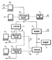
- This object is achieved by the control logic as specified above, which is further characterized by the fact that it comprises at least one assembly constituted by a master processor, two slave processors each managing half of the connection modules and each connected to a memory, an exchange memory linked to a common memory and on the one hand to the slave processors by a bus coupler and on the other hand to the master processor, an interprocessor coupler connected to each of the escalated processors and to the processor master, and an exchange interface connected to the master processor as well as to markers and to a central control unit.
- control logic comprises two identical assemblies, one of which is in service and the other in reserve.
- An assembly essentially comprises a master processor M, an interprocessor coupler 1, an exchange memory 2, a bus coupler 3 and two slave processors A and B.
- the master processor M is connected to a memory 17 and to an exchange interface 18 connected by a link LU to the markers (not shown) of the central and by a link LC to a control member also forming part of the central.
- the master processor M is connected by a bus 5 to the interprocessor coupler 1 and to the exchange memory 2.
- the interprocessor coupler is connected by status links 6 and 6 'to each of the slave processors A and B; the slave processors A and B have access to the common memory 7 via the bus coupler 3.
- the slave processor A is connected to a program memory 8, and by a bus 10 to four connection modules.
- the slave processor B is connected to a program memory 9, and to four other connection modules by a bus 11.
- the bus coupler 3 is connected by a bus 12 to the slave processor A, and by a bus 13 to the slave processor B; it is also connected by a bus 14 to the exchange memory 2 and to the common memory 7.
- This common memory 7 is composed of a working memory area and a table area for processing telephone signaling.
- the exchange memory 2 allows the exchanges between the master processor M and the slave processors A and B via the bus coupler 3.
- the master processor M and the slave processors A and B are identical, and the memories 7, 8, 9 and 17 are identical.
- this other logic control assembly manages the same connection modules as those managed by the slave processors A and B of the figure.
- the two logic control assemblies therefore do not operate simultaneously; the command to switch from one logic control unit to the other is performed by a single selection circuit 4, shown in the figure; it is connected to each master processor; the link 15 therefore indicates the link with the master processor of the other logic assembly.
- the exchange memories 2 of each logic control unit is connected to the other logic control unit by a bus 16.
- the bus coupler 3 performs two functions: the first relates to the creation of timers for each of the slave processors A and B, and the second relates to the coupling of the address bus and data bus accesses of the two slave processors to the common memory 7.
- the elaboration of the timers is carried out from the data received from each slave processor; the interprocessor coupler can memorize 2000 timers which corresponds to 2 timers per time channel.
- the access of the slave processors to the exchange memory 2 is achieved by regrouping on the one hand the two address buses and on the other hand the two data buses, which constitute the bus 14, each slave processor being connected to the bus coupler 3, by an address bus and a data bus; the exchange memory 2 is therefore connected to the bus coupler by the bus 14 constituted by an address bus and a data bus each obtained by grouping together the address buses and the data buses originating from the slave processors.
- Each grouping is done through doors validated according to the order of arrival of requests for access to exchange memory 2 by slave processors A and B. For the transmission of messages from exchange memory 2 , to the slave processors, doors are used to switch.
- a "not ready” signal is sent to the other slave processor; when the request is satisfied, the "not ready” signal is deleted and the other slave processor can have access to the exchange memory.
- the exchange memory 2 stores the states of the time channels of the equipment of the connection modules and serves as an exchange zone between all the processors; it has a capacity of 8000 words of 9 eb (binary elements) of which 8 eb are used.
- the write and read operations can be controlled by the master processor or by the slave processors; write and read zones are reserved for each of the master and slave processors; for exchanges with another logic control unit (in the case of duplicated control logic), this other logic control set has access, via bus 16, to the exchange memory 2 only for read operations .
- the bus coupler 3 is connected to each slave processor by a bus 12, 13 respectively, each of these buses consisting of a data bus and an address bus.
- the bus coupler 3 performs the grouping of the data buses and the address buses of the buses 12 and 13 to the exchange memory 2 and the common memory 7; it also provides the routing of the data bus and the address bus of the bus 14, to the address bus and the data bus of each of the buses 12 and 13 for messages intended for the slave processors A and B.
- the exchange memory receives the calls from the master processors M and slaves A and B, and the calls from the other logic control unit by bus 16 which includes a data bus and an address bus buses 5, 14 and 16 are managed according to a cyclical priority.
- the selection circuit 4 makes it possible, in the case of duplicated logic, to switch from one logic control unit to another.
- the switchover decision results either from a fault detected in a logic assembly, or from a manual command, or even cyclically without fault detection.
- fault any parameter contributing to the switchover request.
- the logic control unit in service is said to be "Pilot” the other being said to be “Reserve”.
- the selection circuit therefore receives the faults detected by the two logic control assemblies and the manual switching requests. The changeover takes place only if the control logic set in "Reserve” is operational.
- the reception of a switchover request causes a call to the reserve control logic unit, and the switchover is only validated on positive response from this reserve unit.
- the logic control unit performs all the telephony functions: management of state changes before sending them to their destination, calling markers to communicate new calls and hang-ups, transfer of signaling messages.
- a logical connection set is connected to two markers by the LU link, and the exchanges are carried out in a frame of 125 microseconds using the rhythm 0 (1.28 MHz) delivered by the time base of the central office.
- the frame is divided into 32 channels, Vto to Vt31.
- the first half of the frame is reserved for signaling between the markers and the multiplex connection unit via the control logic assembly; an exchange time tn is assigned to a connection module; at time tn 02 call from the first marker to the connection module n, or vice versa; at time tn 04 call from the second marker to the connection module n, or vice versa: the connection test eb is tn 01; the second half of the frame is reserved for sending the message, the channels t16 to t23 being reserved for the first marker, the channels t24 to t31 being reserved for the second marker; an evenness eb is placed at the end of the message, at t23 93 or t31 03; in the event of good reception of the message, the receiving unit transmits in the same frame a eb of "well received", in t23 05 for the first marker, in t31 05 for the second marker; in the event of a lack of impartiality detected by the logic control unit, the latter does not issue a "receipt"; the
- the control logic assembly is also connected to the control member by the LC link.
- the exchanges take place in a frame of 125 microseconds using the rhythm 0; the frame is divided into 32 channels to to t31.
- the first half of the frame transmits the signaling: response calls, positioning; the second half transmits the operating and maintenance messages.
- the call to the control logic unit and the positioning are done, in the first half of the frame, with a call number characterizing the control logic unit.
- the precise destination of the operating and maintenance messages is given in t18 04 and t18 05 according to the following coding: 00 designates a remote connection unit, 01 designates a connection module, 10 designates the control logic, therefore one or the other control logic assembly.
- test command causes the LU links to be replaced by test LU 'links.
Landscapes
- Engineering & Computer Science (AREA)
- Computer Networks & Wireless Communication (AREA)
- Exchange Systems With Centralized Control (AREA)
- Use Of Switch Circuits For Exchanges And Methods Of Control Of Multiplex Exchanges (AREA)
- Hardware Redundancy (AREA)
Claims (6)
Applications Claiming Priority (2)
| Application Number | Priority Date | Filing Date | Title |
|---|---|---|---|
| FR7911321A FR2455837A1 (fr) | 1979-05-04 | 1979-05-04 | Logique de commande d'une unite de raccordement de multiplex dans un central de commutation temporelle |
| FR7911321 | 1979-05-04 |
Publications (2)
| Publication Number | Publication Date |
|---|---|
| EP0018616A1 EP0018616A1 (de) | 1980-11-12 |
| EP0018616B1 true EP0018616B1 (de) | 1983-11-30 |
Family
ID=9225065
Family Applications (1)
| Application Number | Title | Priority Date | Filing Date |
|---|---|---|---|
| EP80102279A Expired EP0018616B1 (de) | 1979-05-04 | 1980-04-28 | Steuerlogik für eine Multiplexverbindungseinheit in einer Zeitmultiplexvermittelungstelle |
Country Status (12)
| Country | Link |
|---|---|
| US (1) | US4354262A (de) |
| EP (1) | EP0018616B1 (de) |
| JP (1) | JPS55150695A (de) |
| CA (1) | CA1150430A (de) |
| DE (1) | DE3065754D1 (de) |
| FI (1) | FI74862C (de) |
| FR (1) | FR2455837A1 (de) |
| IE (1) | IE49778B1 (de) |
| MX (1) | MX146858A (de) |
| PL (1) | PL126398B1 (de) |
| RO (1) | RO80909A (de) |
| ZA (1) | ZA802657B (de) |
Families Citing this family (13)
| Publication number | Priority date | Publication date | Assignee | Title |
|---|---|---|---|---|
| IN155236B (de) * | 1981-03-20 | 1985-01-12 | Gould Inc | |
| US4527266A (en) * | 1982-04-22 | 1985-07-02 | International Telephone And Telegraph Corporation | Interface circuit for use in a distributed processing switch unit |
| US4549273A (en) * | 1982-12-10 | 1985-10-22 | Ael Microtel Limited | Memory access control circuit |
| FR2541063B1 (fr) * | 1983-02-14 | 1986-03-21 | Telecommunications Sa | Terminal semaphore multiligne |
| US4698746A (en) * | 1983-05-25 | 1987-10-06 | Ramtek Corporation | Multiprocessor communication method and apparatus |
| US4530090A (en) * | 1983-07-29 | 1985-07-16 | International Standard Electric Corporation | Telecommunications systems with user programmable features |
| SE440580B (sv) * | 1983-12-15 | 1985-08-05 | Ericsson Telefon Ab L M | Anordning vid digitalt telefonsystem |
| JPS61166668A (ja) * | 1985-01-19 | 1986-07-28 | Panafacom Ltd | 多重プロセツサ制御方式 |
| JPS62295168A (ja) * | 1986-06-13 | 1987-12-22 | Canon Inc | 機器制御装置 |
| FR2671884A1 (fr) * | 1991-01-17 | 1992-07-24 | Moulinex Sa | Procede d'attribution d'adresses dans un reseau domotique. |
| JP3890266B2 (ja) * | 2002-07-03 | 2007-03-07 | キヤノン株式会社 | ブロックポリマー化合物、インク組成物、分散性組成物及び画像形成方法並びに画像形成装置 |
| EP2564322A4 (de) * | 2010-04-30 | 2017-03-08 | Hewlett-Packard Enterprise Development LP | Transfer von verwaltungsdaten zwischen prozessoren |
| PL425290A1 (pl) | 2018-04-20 | 2019-10-21 | Bombardier Transportation (Zwus) Polska Spółka Z Ograniczoną Odpowiedzialnością | Sposób trwałej regulacji napięcia elementów sprężystych dla zastosowań w warunkach dynamicznych obciążeń |
Family Cites Families (5)
| Publication number | Priority date | Publication date | Assignee | Title |
|---|---|---|---|---|
| GB1168086A (en) * | 1965-11-01 | 1969-10-22 | Kokusai Denshin Denwa Co Ltd | Time Divisional Accumulation and Distribution System for Digital Information |
| CH570092A5 (de) * | 1970-09-18 | 1975-11-28 | Lannionnais Electronique | |
| FR2346930A1 (fr) * | 1976-03-31 | 1977-10-28 | Cit Alcatel | Autocommutateur a reseau de connexion temporel |
| US4150335A (en) * | 1977-08-22 | 1979-04-17 | Communications Satellite Corporation | Highly reliable distribution control unit with improved control capability |
| US4127742A (en) * | 1977-09-01 | 1978-11-28 | International Telephone And Telegraph Corporation | Time division telecommunication system |
-
1979
- 1979-05-04 FR FR7911321A patent/FR2455837A1/fr active Granted
-
1980
- 1980-04-28 FI FI801371A patent/FI74862C/fi not_active IP Right Cessation
- 1980-04-28 EP EP80102279A patent/EP0018616B1/de not_active Expired
- 1980-04-28 CA CA000350808A patent/CA1150430A/fr not_active Expired
- 1980-04-28 DE DE8080102279T patent/DE3065754D1/de not_active Expired
- 1980-05-02 IE IE897/80A patent/IE49778B1/en not_active IP Right Cessation
- 1980-05-02 ZA ZA00802657A patent/ZA802657B/xx unknown
- 1980-05-03 PL PL1980223989A patent/PL126398B1/pl unknown
- 1980-05-05 RO RO80101040A patent/RO80909A/ro unknown
- 1980-05-05 US US06/146,853 patent/US4354262A/en not_active Expired - Lifetime
- 1980-05-06 JP JP6047980A patent/JPS55150695A/ja active Granted
- 1980-05-06 MX MX182201A patent/MX146858A/es unknown
Non-Patent Citations (1)
| Title |
|---|
| Commutation et Electronique No. 34, juillet 1971, pages 25 à 47 * |
Also Published As
| Publication number | Publication date |
|---|---|
| EP0018616A1 (de) | 1980-11-12 |
| PL223989A1 (de) | 1981-02-27 |
| ZA802657B (en) | 1981-05-27 |
| IE49778B1 (en) | 1985-12-11 |
| FR2455837A1 (fr) | 1980-11-28 |
| JPS55150695A (en) | 1980-11-22 |
| DE3065754D1 (en) | 1984-01-05 |
| FI74862B (fi) | 1987-11-30 |
| FI74862C (fi) | 1988-03-10 |
| JPH0154920B2 (de) | 1989-11-21 |
| PL126398B1 (en) | 1983-07-30 |
| CA1150430A (fr) | 1983-07-19 |
| US4354262A (en) | 1982-10-12 |
| FR2455837B1 (de) | 1982-05-07 |
| IE800897L (en) | 1980-11-04 |
| MX146858A (es) | 1982-08-25 |
| FI801371A (fi) | 1980-11-05 |
| RO80909A (ro) | 1983-02-01 |
Similar Documents
| Publication | Publication Date | Title |
|---|---|---|
| EP0018616B1 (de) | Steuerlogik für eine Multiplexverbindungseinheit in einer Zeitmultiplexvermittelungstelle | |
| JP2846314B2 (ja) | 分散制御交換システム内での電話番号翻訳 | |
| JP3014694B2 (ja) | 分散制御交換システム内での経路ハンティング | |
| JP2723217B2 (ja) | 分散制御交換システム内でのシーケンス呼の処理 | |
| JP2935364B2 (ja) | 分散制御交換システムにおける多重ポートハントグループ呼の処理方法 | |
| US6104803A (en) | Intelligent service peripheral device | |
| NO154290B (no) | Fremgangsmùte for oppnùelse av fordelt styring i et kommun ikasjonssystem med et digitalt svitsjenettverk, samt kommu nikasjonssystem for utf!relse av denne fordelte styringsfu nksjon. | |
| DK156320B (da) | Ekspanderbart digitalt koblingsnetvaerk | |
| BG63358B1 (bg) | Разширяема телекомуникационна система | |
| AU6017394A (en) | Telecommunication switch with programmable communications services | |
| WO1992005643A1 (en) | Modular digital telephone system with fully distributed local switching and control | |
| USH1882H (en) | System and method for transferring data to redundant components | |
| JP2723218B2 (ja) | 分散制御交換システム内での分散データベースを使用しての終端ポートの決定 | |
| JPS6370635A (ja) | 電気通信網 | |
| JPH0578219B2 (de) | ||
| US6594685B1 (en) | Universal application programming interface having generic message format | |
| CA1178698A (fr) | Groupe d'unites de terminaux pour autocommutateur numerique | |
| EP0075248B1 (de) | Signalverteilervorrichtung für ein automatisches Zeitmultiplexvermittlungssystem | |
| JP2776977B2 (ja) | Isdn通信システムの障害処理方法およびisdn通信システム | |
| EA004212B1 (ru) | Система обработки данных | |
| USH1802H (en) | System and method for automatically provisioning a telecommunications switch | |
| US7020077B2 (en) | Cross-connect matrix task prioritizer | |
| US5787087A (en) | Method and apparatus for interconnecting a plurality of terminal equipments to the ISDN | |
| US4399534A (en) | Dual rail time and control unit for a duplex T-S-T-digital switching system | |
| US4399369A (en) | Dual rail time and control unit for a duplex T-S-T-digital switching system |
Legal Events
| Date | Code | Title | Description |
|---|---|---|---|
| PUAI | Public reference made under article 153(3) epc to a published international application that has entered the european phase |
Free format text: ORIGINAL CODE: 0009012 |
|
| AK | Designated contracting states |
Designated state(s): BE CH DE FR GB IT NL SE |
|
| 17P | Request for examination filed |
Effective date: 19810427 |
|
| ITF | It: translation for a ep patent filed |
Owner name: JACOBACCI & PERANI S.P.A. |
|
| GRAA | (expected) grant |
Free format text: ORIGINAL CODE: 0009210 |
|
| AK | Designated contracting states |
Designated state(s): BE CH DE FR GB IT LI NL SE |
|
| REF | Corresponds to: |
Ref document number: 3065754 Country of ref document: DE Date of ref document: 19840105 |
|
| PLBE | No opposition filed within time limit |
Free format text: ORIGINAL CODE: 0009261 |
|
| STAA | Information on the status of an ep patent application or granted ep patent |
Free format text: STATUS: NO OPPOSITION FILED WITHIN TIME LIMIT |
|
| 26N | No opposition filed | ||
| PGFP | Annual fee paid to national office [announced via postgrant information from national office to epo] |
Ref country code: CH Payment date: 19910117 Year of fee payment: 12 |
|
| PGFP | Annual fee paid to national office [announced via postgrant information from national office to epo] |
Ref country code: BE Payment date: 19910124 Year of fee payment: 12 |
|
| PG25 | Lapsed in a contracting state [announced via postgrant information from national office to epo] |
Ref country code: CH Effective date: 19920430 Ref country code: BE Effective date: 19920430 Ref country code: LI Effective date: 19920430 |
|
| BERE | Be: lapsed |
Owner name: CIE INDUSTRIELLE DES TELECOMMUNICATIONS CIT-ALCAT Effective date: 19920430 |
|
| REG | Reference to a national code |
Ref country code: CH Ref legal event code: PL |
|
| ITTA | It: last paid annual fee | ||
| PGFP | Annual fee paid to national office [announced via postgrant information from national office to epo] |
Ref country code: FR Payment date: 19931230 Year of fee payment: 15 |
|
| PGFP | Annual fee paid to national office [announced via postgrant information from national office to epo] |
Ref country code: SE Payment date: 19940127 Year of fee payment: 15 |
|
| PGFP | Annual fee paid to national office [announced via postgrant information from national office to epo] |
Ref country code: GB Payment date: 19940221 Year of fee payment: 15 |
|
| PGFP | Annual fee paid to national office [announced via postgrant information from national office to epo] |
Ref country code: DE Payment date: 19940416 Year of fee payment: 15 |
|
| PGFP | Annual fee paid to national office [announced via postgrant information from national office to epo] |
Ref country code: NL Payment date: 19940430 Year of fee payment: 15 |
|
| EAL | Se: european patent in force in sweden |
Ref document number: 80102279.9 |
|
| PG25 | Lapsed in a contracting state [announced via postgrant information from national office to epo] |
Ref country code: GB Effective date: 19950428 |
|
| PG25 | Lapsed in a contracting state [announced via postgrant information from national office to epo] |
Ref country code: SE Effective date: 19950429 |
|
| PG25 | Lapsed in a contracting state [announced via postgrant information from national office to epo] |
Ref country code: NL Effective date: 19951101 |
|
| PG25 | Lapsed in a contracting state [announced via postgrant information from national office to epo] |
Ref country code: FR Effective date: 19951229 |
|
| NLV4 | Nl: lapsed or anulled due to non-payment of the annual fee |
Effective date: 19951101 |
|
| GBPC | Gb: european patent ceased through non-payment of renewal fee |
Effective date: 19950428 |
|
| PG25 | Lapsed in a contracting state [announced via postgrant information from national office to epo] |
Ref country code: DE Effective date: 19960103 |
|
| EUG | Se: european patent has lapsed |
Ref document number: 80102279.9 |
|
| REG | Reference to a national code |
Ref country code: FR Ref legal event code: ST |