EP0010983B1 - Stellgerät - Google Patents
Stellgerät Download PDFInfo
- Publication number
- EP0010983B1 EP0010983B1 EP79302438A EP79302438A EP0010983B1 EP 0010983 B1 EP0010983 B1 EP 0010983B1 EP 79302438 A EP79302438 A EP 79302438A EP 79302438 A EP79302438 A EP 79302438A EP 0010983 B1 EP0010983 B1 EP 0010983B1
- Authority
- EP
- European Patent Office
- Prior art keywords
- wafer
- transducer
- voltage
- article
- acceleration
- Prior art date
- Legal status (The legal status is an assumption and is not a legal conclusion. Google has not performed a legal analysis and makes no representation as to the accuracy of the status listed.)
- Expired
Links
Images
Classifications
-
- H—ELECTRICITY
- H02—GENERATION; CONVERSION OR DISTRIBUTION OF ELECTRIC POWER
- H02N—ELECTRIC MACHINES NOT OTHERWISE PROVIDED FOR
- H02N2/00—Electric machines in general using piezoelectric effect, electrostriction or magnetostriction
- H02N2/02—Electric machines in general using piezoelectric effect, electrostriction or magnetostriction producing linear motion, e.g. actuators; Linear positioners ; Linear motors
- H02N2/021—Electric machines in general using piezoelectric effect, electrostriction or magnetostriction producing linear motion, e.g. actuators; Linear positioners ; Linear motors using intermittent driving, e.g. step motors, piezoleg motors
- H02N2/025—Inertial sliding motors
-
- H—ELECTRICITY
- H02—GENERATION; CONVERSION OR DISTRIBUTION OF ELECTRIC POWER
- H02N—ELECTRIC MACHINES NOT OTHERWISE PROVIDED FOR
- H02N2/00—Electric machines in general using piezoelectric effect, electrostriction or magnetostriction
- H02N2/0095—Electric machines in general using piezoelectric effect, electrostriction or magnetostriction producing combined linear and rotary motion, e.g. multi-direction positioners
-
- H—ELECTRICITY
- H02—GENERATION; CONVERSION OR DISTRIBUTION OF ELECTRIC POWER
- H02N—ELECTRIC MACHINES NOT OTHERWISE PROVIDED FOR
- H02N2/00—Electric machines in general using piezoelectric effect, electrostriction or magnetostriction
- H02N2/02—Electric machines in general using piezoelectric effect, electrostriction or magnetostriction producing linear motion, e.g. actuators; Linear positioners ; Linear motors
- H02N2/06—Drive circuits; Control arrangements or methods
- H02N2/065—Large signal circuits, e.g. final stages
- H02N2/067—Large signal circuits, e.g. final stages generating drive pulses
Definitions
- the present invention relates to positioning apparatus, and in particular to positioning apparatus in which an article is moved by the application of voltages to piezoelectric transducers.
- the invention is applicable to positioning apparatus of various kinds, but one particular application which will herein be described is in the relative positioning of exposure masks and/or substrate wafers in the fabrication of microlithographically generated circuits.
- the known lithographic techniques for fabricating microcircuits requires the accurate alignment of the substrate wafer with respect to the exposure mask.
- simple mechanical, screw-type, means for aligning the mask and the wafer have been used to align the translational and rotational positions of the mask and wafer.
- inevitable tolerances and torques build-up which affect the alignment.
- This electromechanical method for aligning the mask and substrate wafers envisions using a piezoelectric transducer coupled to the mask or wafer to displace one of them with respect to the other in response to a voltage applied to the transducer.
- a piezoelectric transducer coupled to the mask or wafer to displace one of them with respect to the other in response to a voltage applied to the transducer.
- the displacement of the transducer varies directly with the applied voltage, so that precise electromechanical control of the mask or wafer may be exercised by means of precise voltage control.
- the linearity of transducer displacement with respect to voltage breaks down, and so the operating range of the transducer, and therefore the total displacement of the wafer, is limited.
- the present invention also makes use of one or more piezoelectric transducers, but instead of these being supplied with a steady voltage corresponding to the required displacement, they are supplied with a voltage of asymmetrical waveform.
- the transducers are coupled through frictionally engaged surfaces to the wafer or other article to be positioned, and the waveform is such that the acceleration for part of the voltage cycle exceeds the critical acceleration so that relative movement of the frictionally engaged surfaces takes place.
- Each waveform cycle thus produces a net overall change in position of the article.
- the voltage source may comprise a reversible DC supply which may be switched to charge and discharge the capacity of the piezoelectric device through resistors of different values, so producing different charge and discharge rates,
- a continuous cyclic supply having an asymmetric waveform may be employed, and a suitable waveform may be generated by full wave rectification of a sinusoidal alternating voltage.
- a set of four transducers may be employed spaced equidistantly round a cycle and acting in directions tangential to it, and this arrangement, with suitable energisation, will enable a flat article to be translated in two axes and to rotate about a third axis at right angles to its plane.
- the article support may be in the form of hollow tubes to which a vacuum source may be connected to urge the article move strongly towards the support, so that by varying the vacuum the frictional engagement between the article and the support, and so the speed of movement, may be regulated.
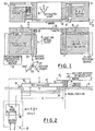
- the alignment fixtures 10 includes a support plate 11 to which is attached an exposure mask 12, and which is provided with levelling screws 13 and springs 14 for adjusting the exposure mask 12 with respect to a reference, or a substrate wafer 15 supported by a further base plate 16 of the alignment fixture 10.
- the levelling screws 13 and springs 14 allow the mask to be rotated about two mutually perpendicular axes (x, y) and to be translated, in this figure vertically, with respect to the substrate wafer 15, along a third axis (z) perpendicular to the other axes.
- the substrate wafer 15 can also be translated along the two mutually perpendicular axes (x, y), which are more clearly shown in Figure 3, and the wafer is also rotatable about the vertical axis (z).
- the wafer 15 is optically aligned with the mask 12 in a conventional manner.
- the wafer 15 is illuminated from below such that when viewed from a position vertically above the mask 12 a diffraction pattern resulting from grids formed on the respective mask and wafer (not shown) may be observed, as indicated by the illumination arrow A and diffraction arrow B in the Figure.
- the substrate wafer 15 is coupled to a piezoelectric transducer 17 which, in accordance with this invention as explained hereinafter, effects the movement of the wafer. It is apparent that the mask 12 could also, or alternatively, be coupled for movement to a transducer in accordance with the invention.
- the piezoelectric transducer 17, in the preferred embodiment of this invention a PZT transducer, is affixed at one end 18 ( Figure 2), by suitable means such as adhesive 19 to the base plate 16.
- the other or free end 20 is frictionally coupled by a support 22 to the substrate wafer 15.
- a voltage source 21 is connected across the transducer 17.
- a plurality of transducers coupled to respective voltage sources are utilised in accordance with this invention to affect the desired displacement and/or rotation of the substrate wafer 15 with respect to the mask 12 or any other suitable reference.
- a change in length (AX) of the transducer 17 of length (L), thickness (T), and inverse piezoelectric tensor component (d), wherein the transducer is poled normal to the electrodes, as shown, may be expressed as
- the wafer 15 is coupled to the transducer 17 by a wafer support 22.
- the wafer support 22 of this invention is affixed, e.g. by adhesive 23 (Figure 2) to the transducer's free end 20.
- One embodiment of the wafer support 22 may take the form of a simple column or support structure 24, or, as shown in Figure 1, the preferred embodiment of the wafer support 22 is a tubular support 25, having one end frictionally coupled to the wafer and the other end coupled via a valve 26, either to a vent 25 open to the local atmospheric pressure acting on the wafer 15, or to a conduit 27 connected to a vacuum pump.
- the tubular support 25 is connected to the local ambient atmospheric pressure via vent 25 when no increased coupling of the wafer 15 to the wafer support 22 is desired.
- the tubular support 25 may be connected to the line 27, to increase the coupling force on the wafer at the support 22.
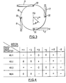
- Figure 3 shows the wafer 15 in plan view, coupled to four piezoelectric transducers 17, in pairs at opposite ends of two diameters of the wafer 15, and acting perpendicular to these diameters. This arrangement allows translation along the x, y axes and rotation about the z axis.
- Figure 4 is a table showing how the transducers need to be energised for the various modes of translation and rotation.
- the potential difference applied to the transducer determines the displacement of the wafer support 22, and therefore that of the wafer, provided the potential difference is below the breakdown voltage of the transducer.
- a displacement of about 1 pm per 100 volts is typical.
- wafer-mask adjustments of ⁇ 0.1 ym are required, and this accuracy is easily obtainable.
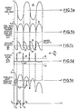
- Figure 5a shows a sine wave voltage 30 supplied to the voltage source means 21 of Figure 2, and converted by a full-wave rectifier 28 into the full-wave rectified voltage 31 of Figure 5b.
- the peak potential difference of Figure 5b is less than the transducer's breakdown voltage.
- the displacement AX is proportional to the applied potential difference and accordingly, the waveform of Figure 5b is proportional to, and also represents, the displacement of transducer 17 and support 22.
- the full-wave rectified wave form 31 ( Figure 5b) provides a driving signal which causes a jogging motion of the wafer in accordance with this invention as it provides an asymmetrical acceleration, as will be described with reference to Figure 6.
- the velocity 32 of the support 22 is proportional to the slope of the displacement ⁇ X of Figure 5b as shown.
- This velocity waveform 32 is periodic and smoothly continuous from maximum positive to maximum negative, but nearly discontinuous from maximum negative to maximum positive as shown at 33.
- the derivative of this velocity acceleration 34 shown in Figure 5d includes a "spike" 35 at each near-discontinuity 33 in the velocity waveform 32, and intervening portions 36 of relatively small amplitude during the smoothly continuous portions of the velocity curve 32.
- the displacement of the transducer is proportional to the voltage, but net motion of the wafer 15 occurs because at the time of the near-discontinuity 33 the inertial force of the wafer opposing the driving force of the transducer exceeds the frictional shear force coupling the wafer 15 to the transducer 17 at the wafer support 22. That is, the critical acceleration (a c ) of the wafer is exceeded by the sharp spike 35 of the asymmetrical accelera - tion 34 of the transducer.
- the critical acceleration of the wafer (a c ) corresponds to the frictional coupling threshold, which may be calculated knowing the coefficient of static friction n s between the wafer 15 and the support 22, the normal coupling force F e and the mass of the wafer M W .
- the critical acceleration may be expressed as:
- the critical acceleration a c is indicated in Figure 5d where it is easily seen that the sharp acceleration spikes 35 exceed the critical acceleration of the wafer, whereas the remaining portions 36 of the acceleration curve 34 do not exceed the critical acceleration.
- the wafer 15 follows the transducer 17.
- slip takes place between the wafer and its support. The inertial force of the wafer moves the wafer, at this time, without regard for the motion of the transducer.
- Figure 6 indicates motion of one transducer 17 (for clarity purposes) and associated wafer 15 portion at six successive time intervals.
- Figures 5b and 6a indicate that the transducer 17 is at its maximum deflection, ⁇ X m , indicated as point X 1 in Figure 6a, and a movement in the negative direction is desired. Also, at time t 1 the transducer velocity (Figure 5c) is zero and increasing negatively, and the transducer acceleration (Figure 5d) is at its maximum for the portion 36 of the acceleration curve.
- the transducer displacement (curve 31 of Figure 5b) is decreasing, the velocity (curve 32 of Figure 5c) increases to its maximum in the negative direction, and because the critical acceleration a c has not been exceeded and the voltage potential is not greater than the breakdown voltage the wafer displacement decreases lineraly (in the analogue mode fashion).
- the minimum deflection of the transducer is reached at the point X 2 ( Figure 6b) corresponding to a change of ⁇ X m , and with the start of the next periodic wave the transducer's velocity 32 changes from maximum negative to maximum positive at the near-discontinuity 33, resulting in the acceleration spike 35.
- the wafer 15 has moved to point X 3 , a distance ⁇ 1 X, negatively, equal to the wafer's negative velocity at the moment the transducer breaks free times the time interval, (t 3 ⁇ t 2 ), while the support 22 has moved in the positive direction from the initial attachment point Y 1 a distance equal to the transducer's positive decreasing velocity 32 ( Figure 5b) times the time interval (t 3 ⁇ t 2 ) to the new attachment point Y Z .
- the maximum voltage of waveform 31 is reached corresponding to the maximum deflection of the transducer 17 and the support 22, back to the point X 1 , point Y 2 of the wafer having moved to the initial point X 1 .
- the critical acceleration is exceeded, the wafer-transducer support frictional coupling is overcome, the wafer continues negatively at its negative velocity times the time interval (t 5 ⁇ t 6 ) for a distance equal to EI X again, and the wafer support moves positively in accordance with the velocity curve 32 a distance equal to E2 X to a new attachment point Y 3 , as shown in Figure 5e and 6f.
- the positive value full wave rectified voltage 31 displaces the wafer 15 in the negative direction in a "jogging" fashion, i.e., increasing then decreasing, such that the net displacement for a given time period or set of pulses exceeds the maximum displacement obtainable by the transducer 17 in the analogue mode of operation.
- motion of the wafer 15 along the x and y axes or rotation about the z axis may be obtained by positive or negative full wave rectified voltage inputs to suitably chosen transducers.
- transducers #1 and #3 are not activated, as represented by a "0”
- transducers #2 and #4 are activated as represented by a "+”, positively and "-", negatively, respectively.
- the wafer critical acceleration a e is a function of the normal coupling force F c , or the frictional coupling. Therefore, the tubular support 25 of Figure 1 may be coupled to a vacuum or low pressure, relative to the local wafer atmospheric pressure, via the valve 26, which may be an electrically controlled valve, in order to adjust the coupling force.
- the invention enables an object such as a wafer 15 to be moved through a distance greater than the maximum movement of a transducer attached to it.
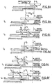
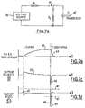
- FIG. 7a A further embodiment of this invention is shown in Figure 7a, and will be described with reference to the waveforms in Figures 7b to 7d.
- the jogging action is performed by means of one or more single pulses.
- the apparatus of Figure 7a includes a reversible D.C. voltage source 40 coupled to a transducer 42 of capacitance C by a switch 41, which may be an electronic switch , through a first resistor R1, through which the transducer is charged.
- the switch 41 than disconnects the voltage source 40 and resistor Rl from the transducer 42 and discharges the transducer through a second resistor R2.
- the charging voltage curve 43 of the RC circuit is chosen to be significantly different from the voltage curve 44 during discharge of the transducer 42 by appropriately choosing the values of R, and R 2 .
- Figures 7c and 7d respectively show the velocity and acceleration curves; the voltage waveforms 43 and 44 result in an asymmetrical velocity 45, 46 and, more importantly, an asymmetrical acceleration 47, 48 wherein a sharp "spike" 49 significantly greater than the critical acceleration Be is obtainable.
- the wafer moves as explained above, and follows the single pulse charging voltage 45.
- Use of piezoelectric transducers in this invention serves to provide precise electromechanical control of the wafer 15, thereby eliminating the need for applying extraneous torques to the wafer as in the prior art. Piezoelectric transducers are advantageous in providing electrical control of the position of the wafer 15 by means of direct coupling thereto without intervening means such as motors, gears or levers.
Landscapes
- Exposure And Positioning Against Photoresist Photosensitive Materials (AREA)
- Container, Conveyance, Adherence, Positioning, Of Wafer (AREA)
- Exposure Of Semiconductors, Excluding Electron Or Ion Beam Exposure (AREA)
- General Electrical Machinery Utilizing Piezoelectricity, Electrostriction Or Magnetostriction (AREA)
Claims (6)
Applications Claiming Priority (2)
| Application Number | Priority Date | Filing Date | Title |
|---|---|---|---|
| US05/958,273 US4195243A (en) | 1978-11-06 | 1978-11-06 | Piezoelectric wafer mover |
| US958273 | 1978-11-06 |
Publications (2)
| Publication Number | Publication Date |
|---|---|
| EP0010983A1 EP0010983A1 (de) | 1980-05-14 |
| EP0010983B1 true EP0010983B1 (de) | 1983-07-13 |
Family
ID=25500804
Family Applications (1)
| Application Number | Title | Priority Date | Filing Date |
|---|---|---|---|
| EP79302438A Expired EP0010983B1 (de) | 1978-11-06 | 1979-11-05 | Stellgerät |
Country Status (5)
| Country | Link |
|---|---|
| US (1) | US4195243A (de) |
| EP (1) | EP0010983B1 (de) |
| JP (1) | JPS5574138A (de) |
| CA (1) | CA1115813A (de) |
| DE (1) | DE2965869D1 (de) |
Families Citing this family (48)
| Publication number | Priority date | Publication date | Assignee | Title |
|---|---|---|---|---|
| DE3009975C2 (de) * | 1980-03-14 | 1983-01-27 | Siemens AG, 1000 Berlin und 8000 München | Verfahren zur Impulsanregung eines piezoelektrischen Schall-Sendewandlers |
| DE3040563A1 (de) * | 1980-10-28 | 1982-05-27 | Siemens AG, 1000 Berlin und 8000 München | Elektrisch zu betaetigendes stellglied |
| EP0071666B1 (de) * | 1981-08-10 | 1985-02-06 | International Business Machines Corporation | Elektrische bewegbare Träger |
| DE3610540A1 (de) * | 1986-03-27 | 1987-10-01 | Kernforschungsanlage Juelich | Bewegungseinrichtung zur mikrobewegung von objekten |
| DE3614996C1 (de) * | 1986-05-02 | 1987-07-30 | Leitz Ernst Gmbh | Elektrisch steuerbare Antriebsvorrichtung |
| DE3733783A1 (de) * | 1986-10-06 | 1988-04-14 | Canon Kk | Vibrations-antriebsvorrichtung |
| US4723086A (en) * | 1986-10-07 | 1988-02-02 | Micronix Corporation | Coarse and fine motion positioning mechanism |
| JPS63299785A (ja) * | 1987-05-29 | 1988-12-07 | Res Dev Corp Of Japan | 圧電・電歪素子を用いた衝撃力による微小移動装置 |
| DE3844821C2 (en) * | 1988-07-03 | 1993-07-22 | Kfa Juelich Gmbh, 5170 Juelich, De | Micromanipulator for raster tunnel microscope |
| US5043621A (en) * | 1988-09-30 | 1991-08-27 | Rockwell International Corporation | Piezoelectric actuator |
| US4928030A (en) * | 1988-09-30 | 1990-05-22 | Rockwell International Corporation | Piezoelectric actuator |
| US5039899A (en) * | 1989-02-28 | 1991-08-13 | Brother Kogyo Kabushiki Kaisha | Piezoelectric transducer |
| JPH0688680B2 (ja) * | 1989-03-20 | 1994-11-09 | 輝 林 | 記録媒体搬送装置及びこの装置に用いられる圧電素子付枠体 |
| US5969464A (en) * | 1989-04-18 | 1999-10-19 | Minolta Co., Ltd. | Drive device using electromechanical transducer and an apparatus employing the drive device |
| WO1991004584A1 (en) * | 1989-09-08 | 1991-04-04 | Massachusetts Institute Of Technology | Miniature actuator |
| JPH0487253U (de) * | 1990-11-30 | 1992-07-29 | ||
| JP2905643B2 (ja) * | 1992-05-29 | 1999-06-14 | 住友重機械工業株式会社 | 圧電リニアアクチュエータ |
| JPH0741207B2 (ja) * | 1993-02-18 | 1995-05-10 | インターナショナル・ビジネス・マシーンズ・コーポレイション | マイクロアクチュエータ |
| US5616980A (en) * | 1993-07-09 | 1997-04-01 | Nanomotion Ltd. | Ceramic motor |
| IL106296A0 (en) * | 1993-07-09 | 1993-12-28 | Nanomotion Ltd | Ceramic motor |
| US5432395A (en) * | 1993-08-02 | 1995-07-11 | Bonneville Scientific Incorporated | Direct-drive field actuator motors |
| US5682076A (en) * | 1993-08-03 | 1997-10-28 | Nanomotion Ltd. | Ceramic disc-drive actuator |
| US5589723A (en) * | 1994-03-29 | 1996-12-31 | Minolta Co., Ltd. | Driving apparatus using transducer |
| JPH0821946A (ja) * | 1994-07-08 | 1996-01-23 | Minolta Co Ltd | 電気−機械変換素子を使用したレンズ装置駆動機構 |
| US5629577A (en) | 1994-07-15 | 1997-05-13 | Micro Medical Devices | Miniature linear motion actuator |
| US5587846A (en) * | 1994-07-15 | 1996-12-24 | Minolta Co., Ltd. | Lens moving apparatus |
| JPH0843872A (ja) * | 1994-08-03 | 1996-02-16 | Minolta Co Ltd | 電気−機械変換素子を使用したレンズ駆動装置 |
| US5668432A (en) * | 1995-03-24 | 1997-09-16 | Nippondenso Co., Ltd. | Articulation device |
| US5786654A (en) * | 1995-06-08 | 1998-07-28 | Minolta Co., Ltd. | Movable stage utilizing electromechanical transducer |
| US5675444A (en) * | 1995-07-27 | 1997-10-07 | Minolta Co., Ltd. | Lens barrel having a piezoelectric actuator for moving optical elements |
| JPH09191665A (ja) * | 1996-01-04 | 1997-07-22 | Minolta Co Ltd | 電気−機械変換素子を使用した直線駆動機構 |
| JP3358418B2 (ja) * | 1996-01-04 | 2002-12-16 | ミノルタ株式会社 | 電気−機械変換素子を使用した駆動機構 |
| JPH09247967A (ja) * | 1996-03-06 | 1997-09-19 | Minolta Co Ltd | 電気機械変換素子を使用した駆動装置 |
| GB2316221A (en) * | 1996-08-05 | 1998-02-18 | Karrai Haines Gbr | Positioner using piezoelectric actuator |
| GB2316222B (en) * | 1996-08-05 | 1998-07-01 | Karrai Haines Gbr | Inertial positioner |
| US5986826A (en) * | 1996-12-17 | 1999-11-16 | Minolta Co., Ltd. | Drive device using electromechanical conversion element |
| US6051909A (en) * | 1996-12-27 | 2000-04-18 | Minolta Co., Ltd. | Drive device using electromechanical transducer |
| US6084363A (en) * | 1997-01-17 | 2000-07-04 | Minolta Co., Ltd. | Drive pulse generating apparatus for drive device using electromechanical transducer |
| US6114799A (en) * | 1997-02-10 | 2000-09-05 | Minolta Co., Ltd. | Driving mechanism |
| JP4277384B2 (ja) * | 1999-09-30 | 2009-06-10 | コニカミノルタホールディングス株式会社 | 圧電アクチュエータ |
| GB2369489B (en) * | 2000-11-23 | 2004-03-10 | Khaled Karrai | Inertial rotation device |
| SE520097C2 (sv) * | 2000-12-05 | 2003-05-27 | Nanofactory Instruments Ab | Mikropositioneringsanordning |
| US7053527B2 (en) * | 2003-12-18 | 2006-05-30 | Piezomotor Uppsala Ab | Electromechanical motor and assembling method therefore |
| US20080014720A1 (en) * | 2006-03-16 | 2008-01-17 | Dynatex International | Street smart wafer breaking mechanism |
| US8059346B2 (en) | 2007-03-19 | 2011-11-15 | New Scale Technologies | Linear drive systems and methods thereof |
| KR20130088479A (ko) * | 2012-01-31 | 2013-08-08 | 삼성전자주식회사 | 슬립-스틱방식 압전 구동 장치 |
| JP6401021B2 (ja) * | 2014-11-18 | 2018-10-03 | 株式会社荏原製作所 | 基板洗浄装置、基板処理装置、および基板洗浄方法 |
| US10187037B2 (en) | 2015-08-21 | 2019-01-22 | New Scale Technologies, Inc. | Stick-slip stage device and methods of use thereof |
Family Cites Families (7)
| Publication number | Priority date | Publication date | Assignee | Title |
|---|---|---|---|---|
| US3217218A (en) * | 1962-07-23 | 1965-11-09 | Floyd G Steele | Alternating energy control system |
| US3684904A (en) * | 1969-04-24 | 1972-08-15 | Gennady Vasilievich Galutva | Device for precision displacement of a solid body |
| DE2306232A1 (de) * | 1972-02-09 | 1973-08-23 | Decca Ltd | Antriebseinrichtung |
| US3808488A (en) * | 1972-07-14 | 1974-04-30 | Dynamics Corp Massa Div | Means for making precision microadjustments in the position of a movable element |
| US3902084A (en) * | 1974-05-30 | 1975-08-26 | Burleigh Instr | Piezoelectric electromechanical translation apparatus |
| SE436675B (sv) * | 1975-08-12 | 1985-01-14 | Ki Politekhnichsky I Im 50 Let | Elektrisk motor driven genom piezoelektriska krafter |
| JPS5315060A (en) * | 1976-07-28 | 1978-02-10 | Hitachi Ltd | Inching device |
-
1978
- 1978-11-06 US US05/958,273 patent/US4195243A/en not_active Expired - Lifetime
-
1979
- 1979-10-30 CA CA338,738A patent/CA1115813A/en not_active Expired
- 1979-11-05 EP EP79302438A patent/EP0010983B1/de not_active Expired
- 1979-11-05 DE DE7979302438T patent/DE2965869D1/de not_active Expired
- 1979-11-06 JP JP14429379A patent/JPS5574138A/ja active Granted
Also Published As
| Publication number | Publication date |
|---|---|
| JPS5574138A (en) | 1980-06-04 |
| CA1115813A (en) | 1982-01-05 |
| JPS5738023B2 (de) | 1982-08-13 |
| DE2965869D1 (en) | 1983-08-18 |
| EP0010983A1 (de) | 1980-05-14 |
| US4195243A (en) | 1980-03-25 |
Similar Documents
| Publication | Publication Date | Title |
|---|---|---|
| EP0010983B1 (de) | Stellgerät | |
| Merry et al. | Using a walking piezo actuator to drive and control a high-precision stage | |
| EP0188045A1 (de) | Verformbares Spannfutter | |
| US5877579A (en) | Ceramic motor | |
| KR970705188A (ko) | 소형 선형운동 액튜에이터(Miniature linear motion actuator) | |
| US5418418A (en) | Micro-actuator | |
| EP0166499B1 (de) | Präzisionsbewegungsmechanismus | |
| US7592737B2 (en) | MEMS device comprising an actuator generating a hysteresis driving motion | |
| WO2004008621A1 (en) | Fine control of electromechanical motors | |
| EP0160707B1 (de) | Piezoelektrischer Rotationsschrittantrieb | |
| CA2295819C (en) | Piezoelectric motor | |
| GB2088645A (en) | High speed, high response drive | |
| EP0085745A2 (de) | Feinrotationsmechanismus | |
| Simu et al. | Analysis of quasi-static and dynamic motion mechanisms for piezoelectric miniature robots | |
| CN110661445A (zh) | 一种并联式三自由度压电谐振自致动机构及其激励方法 | |
| Merry et al. | Control of a high precision stage using a walking piezo actuator | |
| JPS6331480A (ja) | 超音波モ−タ | |
| JPS6044838B2 (ja) | 回転微動機構 | |
| JPS6123676B2 (de) | ||
| JP2749682B2 (ja) | 移動テーブル | |
| JP2001147193A (ja) | 接着力測定装置 | |
| JPH05185383A (ja) | 多自由度アクチュエータ | |
| JPS59101834A (ja) | 精密平面移動装置 | |
| JPH0894780A (ja) | x−y−θ微動ステージ | |
| RU2040107C1 (ru) | Пьезокерамический зажим |
Legal Events
| Date | Code | Title | Description |
|---|---|---|---|
| PUAI | Public reference made under article 153(3) epc to a published international application that has entered the european phase |
Free format text: ORIGINAL CODE: 0009012 |
|
| AK | Designated contracting states |
Designated state(s): CH DE FR GB IT NL SE |
|
| 17P | Request for examination filed | ||
| ITF | It: translation for a ep patent filed | ||
| GRAA | (expected) grant |
Free format text: ORIGINAL CODE: 0009210 |
|
| AK | Designated contracting states |
Designated state(s): CH DE FR GB IT NL SE |
|
| REF | Corresponds to: |
Ref document number: 2965869 Country of ref document: DE Date of ref document: 19830818 |
|
| ET | Fr: translation filed | ||
| PLBE | No opposition filed within time limit |
Free format text: ORIGINAL CODE: 0009261 |
|
| STAA | Information on the status of an ep patent application or granted ep patent |
Free format text: STATUS: NO OPPOSITION FILED WITHIN TIME LIMIT |
|
| 26N | No opposition filed | ||
| PGFP | Annual fee paid to national office [announced via postgrant information from national office to epo] |
Ref country code: SE Payment date: 19911022 Year of fee payment: 13 |
|
| PGFP | Annual fee paid to national office [announced via postgrant information from national office to epo] |
Ref country code: DE Payment date: 19911128 Year of fee payment: 13 |
|
| ITTA | It: last paid annual fee | ||
| PGFP | Annual fee paid to national office [announced via postgrant information from national office to epo] |
Ref country code: CH Payment date: 19911219 Year of fee payment: 13 |
|
| PG25 | Lapsed in a contracting state [announced via postgrant information from national office to epo] |
Ref country code: SE Effective date: 19921106 |
|
| PG25 | Lapsed in a contracting state [announced via postgrant information from national office to epo] |
Ref country code: CH Effective date: 19921130 |
|
| REG | Reference to a national code |
Ref country code: CH Ref legal event code: PL |
|
| PG25 | Lapsed in a contracting state [announced via postgrant information from national office to epo] |
Ref country code: DE Effective date: 19930803 |
|
| PGFP | Annual fee paid to national office [announced via postgrant information from national office to epo] |
Ref country code: GB Payment date: 19931011 Year of fee payment: 15 |
|
| PGFP | Annual fee paid to national office [announced via postgrant information from national office to epo] |
Ref country code: FR Payment date: 19931110 Year of fee payment: 15 |
|
| PGFP | Annual fee paid to national office [announced via postgrant information from national office to epo] |
Ref country code: NL Payment date: 19931130 Year of fee payment: 15 |
|
| PG25 | Lapsed in a contracting state [announced via postgrant information from national office to epo] |
Ref country code: GB Effective date: 19941105 |
|
| EUG | Se: european patent has lapsed |
Ref document number: 79302438.1 Effective date: 19930610 |
|
| PG25 | Lapsed in a contracting state [announced via postgrant information from national office to epo] |
Ref country code: NL Effective date: 19950601 |
|
| GBPC | Gb: european patent ceased through non-payment of renewal fee |
Effective date: 19941105 |
|
| NLV4 | Nl: lapsed or anulled due to non-payment of the annual fee | ||
| PG25 | Lapsed in a contracting state [announced via postgrant information from national office to epo] |
Ref country code: FR Effective date: 19950731 |
|
| REG | Reference to a national code |
Ref country code: FR Ref legal event code: ST |