EP0009592B1 - Verfahren und Schaltungsanordnung zur Prüfung einer Nachrichtenstation - Google Patents
Verfahren und Schaltungsanordnung zur Prüfung einer Nachrichtenstation Download PDFInfo
- Publication number
- EP0009592B1 EP0009592B1 EP79103055A EP79103055A EP0009592B1 EP 0009592 B1 EP0009592 B1 EP 0009592B1 EP 79103055 A EP79103055 A EP 79103055A EP 79103055 A EP79103055 A EP 79103055A EP 0009592 B1 EP0009592 B1 EP 0009592B1
- Authority
- EP
- European Patent Office
- Prior art keywords
- signal
- discriminator
- input
- simulated
- dis
- Prior art date
- Legal status (The legal status is an assumption and is not a legal conclusion. Google has not performed a legal analysis and makes no representation as to the accuracy of the status listed.)
- Expired
Links
- 238000012360 testing method Methods 0.000 title claims abstract description 33
- 238000000034 method Methods 0.000 title claims abstract description 14
- 230000001105 regulatory effect Effects 0.000 claims abstract 5
- 238000004088 simulation Methods 0.000 claims description 11
- 230000005540 biological transmission Effects 0.000 claims 1
- 238000010586 diagram Methods 0.000 description 4
- 239000004065 semiconductor Substances 0.000 description 2
- 230000006978 adaptation Effects 0.000 description 1
- 230000003321 amplification Effects 0.000 description 1
- 230000007547 defect Effects 0.000 description 1
- 238000003199 nucleic acid amplification method Methods 0.000 description 1
- 230000010076 replication Effects 0.000 description 1
- 238000010998 test method Methods 0.000 description 1
Images


Classifications
-
- H—ELECTRICITY
- H04—ELECTRIC COMMUNICATION TECHNIQUE
- H04B—TRANSMISSION
- H04B3/00—Line transmission systems
- H04B3/02—Details
- H04B3/20—Reducing echo effects or singing; Opening or closing transmitting path; Conditioning for transmission in one direction or the other
- H04B3/23—Reducing echo effects or singing; Opening or closing transmitting path; Conditioning for transmission in one direction or the other using a replica of transmitted signal in the time domain, e.g. echo cancellers
-
- H—ELECTRICITY
- H04—ELECTRIC COMMUNICATION TECHNIQUE
- H04L—TRANSMISSION OF DIGITAL INFORMATION, e.g. TELEGRAPHIC COMMUNICATION
- H04L1/00—Arrangements for detecting or preventing errors in the information received
- H04L1/24—Testing correct operation
Definitions
- the invention relates to a method for testing a message station, which can optionally be placed in a test state or in an operating state, according to which, in the operating state, a message is fed in duplex mode over a two-wire line to another message station, after which a simulated signal is obtained. compared with the received signal and thus a comparison signal is obtained and fed to the receiver, and then the comparison signal is compared with a constant reference signal and thus a control signal is obtained, with the aid of which the simulated signal is automatically adjusted such that the transmitted message is not disruptive affects the recipient of the own news station.
- Checking a news station - for example by inserting a test loop in the area of this news station - is particularly useful if as many components of this news station are checked. The greater the proportion of those parts of the message station that are not detected during the test, the greater the probability that a defect will not be recognized.
- the invention is based on the object of specifying a method which enables as many parts of a message station as possible to be checked.
- the object is achieved in that the simulated signal is compared with the message in the test state and the simulated signal is automatically set with the control signal obtained in such a way that the message emitted by the own station is received with the receiver of the own station
- the method according to the invention is characterized in that it enables the testing of all essential parts of the message station, in particular the testing of those parts with the aid of which the simulated signal is obtained and readjusted.
- the method is also distinguished by the fact that it can be implemented with a practically negligible little technical outlay.
- the difference between the simulated signal and the received signal is signaled with the comparison signal, then it is expedient that the supply of the received signal is prevented in the test state, so that the simulated signal is equal to the comparison signal. In this way, the function of a comparator, with the aid of which the comparison signal is obtained, is also checked.
- a replication circuit arrangement is provided, to which the message is fed and which emits the simulated signal, that a comparator is provided, which in the operating state depends on the simulated signal and on the received signal the comparison signal generates that a discriminator is provided, which outputs the control signal via its output, which signals the difference between those signals which are present at its first input or at its second input, that a first switch is provided, which in the operating state is a first Takes switch position, in which the constant reference signal is fed to the first input of the discriminator, and in the test state assumes a second switch position, in which the message is fed to the first input of the discriminator that a second switch is provided, which in the operating state has a first switch assumes the position via which the comparison signal is fed to the second input of the discriminator and which in the test state assumes a second switch position in which the simulated signal is fed to the second input of the discriminator.
- the message source NQ emits the message n to be transmitted.
- the simulated signal ns is obtained with the aid of the simulation circuit arrangement NA.
- the simulated signal ns and the received signal are compared with one another in the comparator VGL and the comparison signal vs is obtained. In particular, the difference between the simulated signal ns and the received signal it can be formed with the aid of the comparator VGL.
- the comparison signal vs and a constant reference signal rf compared with one another and a control signal rs is derived, with the aid of which the simulated signal ns is automatically set such that the transmitted message n does not have a disruptive effect in the receiver EM of the message station shown in FIG. 1.
- the message n can be digital and in particular binary. However, it can also be an analog message, for example a voice signal.
- Fig. 2 shows the test state of the message station.
- the simulated signal ns is thus compared with the message n instead of the comparison signal vs shown in FIG. 1 in the discriminator DIS.
- the control signal rs obtained in this way, the simulated signal ns is automatically set such that the message n sent by this own station is received with the receiver EM of the own station.
- the message sent by another station, not shown is received by the receiver EM
- the message n is received by the own station during the test state according to FIG. 2.
- the transmitter SE consists of the voltage source SP and the internal resistance Ri. With the aid of the transmitter SE, both amplification and line adaptation can be carried out.
- the replica circuit arrangement NA can emit either a digital or an analog simulated signal ns on a case-by-case basis.
- the control signal rs is generally digital if the simulation circuit arrangement NA also works digitally. If the simulation circuit arrangement NA operates in an analog manner, the control signal rs can be either analog or digital.
- the discriminator DIS is used to determine the difference between those signals which are present at inputs a and b.
- a summator is generally provided as the comparator VGL, with the aid of which the difference between the simulated signal ns and the received signal is determined.
- VGL the comparator
- the sum of the simulated signal ns and the received signal it should be zero in terms of data signals. If this is the case, then the transmitted message n has no disruptive effect in the receiver EM of the own message station shown in FIG. 3.
- the two switches SW 1 and SW 2 assume the fully drawn switch positions, which are designated by reference numerals 1, during the duration of the normal operating state. During the duration of the test state, the two switches are brought into their second switch positions, shown in dashed lines and designated by the reference symbol 0.
- a constant reference signal rf is fed to the input a of the discriminator DIS via the circuit point P 1.
- the input b of the discriminator receives the comparison signal vs.
- the control signal rs signals the difference between the signals initially input to the discriminator and automatically adjusts the simulation circuit arrangement NA in such a way that the cheapest simulated signal ns results. This simulated signal ns is only effective in the comparator VGL during the duration of the operating state.
- the message a is fed to the input a of the discriminator DIS via the circuit points P 3, P 2 and via the switch SW 1.
- the input b of the discriminator receives the simulated signal ns via the switch SW 2.
- the difference between the message signal n and the simulated signal ns is now determined and the corresponding control signal rs is supplied to the simulation circuit arrangement NA. If the message source NQ, the transmitter SE, the simulation circuit arrangement NA, the discriminator DIS, the receiver EM and the associated connecting lines are in order, then the message n is received in the receiver EM during the test state.
- the receiver EM is thus used in addition to its other function during the test state to test the message station.
- the circuit point P 2 is connected to the connection point P 3 of the voltage source SP and the internal resistance Ri.
- further networks can be arranged between the message source NQ and the point P 3.
- the connection shown between the two points P 2 and P 3 has the advantage that the function of the transmitter SE is also checked.
- the circuit arrangement shown in FIG. 4 differs from the circuit arrangement shown in FIG. 3 only in the somewhat different arrangement of the switch SW 2. It is assumed that a summator is provided as the comparator VGL, with the aid of which the difference between the signals supplied at the beginning ns and it is determined. If the switch SW 2 shown in FIG. 4 assumes its switch position shown in dashed lines in the test state, the supply of the received signal to the comparator VGL is prevented. If the received signal is not supplied, the comparison signal vs the simulated signal ns supplied at the beginning is the same. 3, the simulated signal ns is thus described in the test state fed to the input b of the discriminator DIS.
- the circuit arrangement shown in FIG. 4 is characterized in that the function of the comparator VGL is also checked, in addition to the functions of the other parts of the message station.
- a summator is provided as a comparator, then this can either cause an addition or a subtraction of the two signals ns supplied at the beginning or it can effect it. Depending on the polarity of these signals, the difference between the two signals should be determined in each case. 3 and 4 can work either digitally or analogously, depending on whether they are supplied with digital or analog signals.
- the switches SW 1 and SW 2 can be implemented with the aid of relays, with the aid of push buttons or with the aid of semiconductor switches, in particular with the aid of FET semiconductor components. In general, it is expedient to operate these two switches in a coupled manner so that they act like a double switch and, when actuated, either both assume the switch position shown in full or both assume the switch position shown in broken lines.
- 5 and 6 show block diagrams of news stations, the components of which work predominantly digitally. It can therefore be assumed that the message source NQ emits a digital signal to a digitally operating simulation circuit arrangement NA. This simulation circuit arrangement emits a digital simulated signal ns / d and is controlled with a digital control signal rs / d. The discriminator DIS and the receiver EM also receive digital signals at the beginning.
- an analog signal is derived from the message n.
- the digital / analog converter D / A is therefore required. In this case, it would be easier to interrupt the conductive connection of the points P 2 and P 3 via the digital / analog converter and to connect the points P 2 and P 4 directly to one another.
- the analog / digital converter A / D is required to generate the digital received signal es / d.
- the circuit arrangement shown in FIG. 6 differs from that shown in FIG. 5 only in the different arrangement of the switches SW 2.
- a digital message n is again required, but this is converted into an analog signal using the pulse shaper IF.
- the simulation circuit arrangement NA works analogously and emits the analog simulated signal ns / a.
- the received signal is fed to the receiving amplifier EV, via the output of which an analog signal is again emitted.
- Two analog signals are thus present at the two inputs of the comparator VGL and an analog comparator VGL is required.
- Analog signals are also supplied to the receiver EM and the discriminator DIS.
- the control signal rs emitted by the discriminator could in principle either be a digital signal or an analog signal. It would be conceivable for a further discriminator DIS 2, which responds to two or more threshold values, to be connected between the comparator VGL and the receiver EM, whereas the discriminator DIS responds only to a single threshold value.
- FIGS. 9 and 10 show block diagrams of news stations, the components of which partly work digitally and partly analog. These two circuit arrangements are characterized by particularly low technical complexity.
- a digital message n is again required and a digitally operating replica circuit arrangement NA.
- the digital simulated signal ns / d is converted into an analog simulated signal ns / a with the aid of the digital / analog converter D / A. Since the received signal is again an analog signal and an analog signal is also output via the output of the receiving amplifier ev, two analog signals are compared with one another in the comparator VGL and an analog comparison signal is output at the input b of the discriminator DIS.
Landscapes
- Computer Networks & Wireless Communication (AREA)
- Signal Processing (AREA)
- Engineering & Computer Science (AREA)
- Monitoring And Testing Of Transmission In General (AREA)
- Communication Control (AREA)
- Coupling Device And Connection With Printed Circuit (AREA)
- Monitoring And Testing Of Exchanges (AREA)
- Small-Scale Networks (AREA)
- Data Exchanges In Wide-Area Networks (AREA)
- Dc Digital Transmission (AREA)
- Mobile Radio Communication Systems (AREA)
- Financial Or Insurance-Related Operations Such As Payment And Settlement (AREA)
- Transition And Organic Metals Composition Catalysts For Addition Polymerization (AREA)
- Maintenance And Management Of Digital Transmission (AREA)
- Circuits Of Receivers In General (AREA)
Description
- Die Erfindung bezieht sich auf ein Verfahren zur Prüfung einer Nachrichtenstation, die wahlweise in einen Prüfzustand oder in einen Betriebszustand versetzbar ist, wonach im Betriebszustand eine Nachricht im Duplex-Betrieb über eine Zweidraht-Leitung einer anderen Nachrichtenstation zugleitet wird, wonach ein nachgebildetes Signal gewonnen, mit dem empfangenen Signal verglichen und so ein Vergleichssignal gewonnen und dem Empfänger zugeführt wird, und wonach das Vergleichssignal mit einem konstanten Referenzsignal verglichen und so ein Regelsignal gewonnen wird, mit dessen Hilfe das nachgebildete Signal automatisch derart eingestellt wird, daß sich die gesendete Nachricht nicht störend auswirkt im Empfänger der eigenen Nachrichtenstation.
- Die Überprüfung einer Nachrichtenstation - beispielsweise durch Einlegen einer Prüfschleife im Bereich dieser Nachrichtenstation - ist speziell dann sinnvoll, wenn möglichst viele Bestandteile dieser Nachrichtenstation geprüft werden. Je größer der Anteil jener Teile der Nachrichtenstation ist, die bei der Prüfung nicht erfaßt werden, desto größer ist die Wahrscheinlichkeit, daß ein Defekt nicht erkannt wird.
- Der Erfindung liegt die Aufgabe zugrunde, ein Verfahren anzugeben, das eine Prüfung möglichst vieler Teile einer Nachrichtenstation ermöglicht.
- Erfindungsgemäß wird die Aufgabe dadurch gelöst, daß im Prüfzustand das nachgebildete Signal mit der Nachricht verglichen wird und mit dem dabei gewonnenen Regelsignal das nachgebildete Signal automatisch derart eingestellt wird, daß mit dem Empfänger der eigenen Station die von der eigenen Station abgegebene Nachricht empfangen wird
- Das erfindungsgemäße Verfahren zeichnet sich dadurch aus, daß es die Prüfung aller wesentlichen Teile der Nachrichtenstation ermöglicht, insbesondere die Prüfung jener Teile, mit Hilfe der das nachgebildete Signal gewonnen und nachgeregelt wird. Das Verfahren zeichnet sich ferner dadurch aus, daß es mit einem praktisch vernachlässigbaren geringen technischen Aufwand realisierbar ist.
- Falls mit dem Vergleichssignal die Differenz des nachgebildeten Signals und des empfangenen Signals signalisiert wird, dann ist es zweckmäßig, daß im Prüfzustand die Zufuhr des empfangenen Signals unterbunden wird, so daß das nachgebildete Signal dem Vergleichssignal gleicht. Auf diese Weise wird also auch die Funktion eines Vergleichers, mit dessen Hilfe das Vergleichssignal gewonnen wird, überprüft.
- Um das Verfahren auf besonders rationelle Weise durchzuführen ist es zweckmäßig, daß eine Nachbildungsschaltungsanordnung vorgesehen ist, der die Nachricht zugeführt wird und die das nachgebildete Signal abgibt, daß ein Vergleicher vorgesehen ist, der im Betriebszustand in Abhängigkeit vom nachgebildeten Signal und in Abhängigkeit vom empfangenen Signal das Vergleichssignal erzeugt, daß ein Diskriminator vorgesehen ist, der über seinen Ausgang das Regelsignal abgibt, das die Differenz jener Signale signalisiert, die an seinem ersten Eingang bzw. an seinem zweiten Eingang anliegen, daß ein erster Schalter vorgesehen ist, der im Betriebszustand eine erste Schalterstellung einnimmt, bei der das konstante Referenzsignal dem ersten Eingang des Diskriminators zugeführt wird, und der im Prüfzustand eine zweite Schalterstellung einnimmt, bei der die Nachricht dem ersten Eingang des Diskriminators zugeführt wird, daß ein zweiter Schalter vorgesehen ist, der im Betriebszustand eine erste Schalterstellung einnimmt, über die das Vergleichssignal dem zweiten Eingang des Diskriminators zugeführt wird und der im Prüfzustand eine zweite Schalterstellung einnimmt, bei der das nachgebildete Signal dem zweiten Eingang des Diskriminators zugeführt wird.
- Im folgenden werden Ausführungsbeispiele der Erfindung an Hand der Fig. 1 bis 10 erläutert, wobei in mehreren Figuren dargestellte gleiche Gegenstände mit gleichen Bezugszeichen bezeichnet sind. Es zeigt
- Fig. 1 ein Blockschaltbild, an Hand dessen der Betriebszustand einer Nachrichtenstation erläutert wird,
- Fig. 2 ein Blockschaltbild, an Hand dessen der Prüfzustand der Nachrichtenstation erläutert wird,
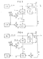
- Fig. 3 und 4 mehrere Schaltungsanordnungen zur Realisierung des Verfahrens in prinzipeller Darstellung,
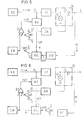
- Fig.5 und 6 mehrere Ausführungsbeispiele von Schaltungsanordnungen zur Realisierung des Verfahrens bei vorwiegend digitaler Verarbeitung der auftretenden Signale,
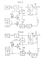
- Fig. 7 und 8 mehrere Schaltungsanordnungen zur Realisierung des Verfahrens bei vorwiegend analoger Verarbeitung der Signale,
- Fig. 9 uf.d 10 besonders bewährte Ausführungsbeispiele zur Realisierung des Verfahrens.
- Fig. 1 zeigt den Betriebszustand einer Nachrichtenstation, die über die Zweidrahtleitung L im Duplexbetrieb mit einer anderen nicht dargestellten Nachrichtenstation verbunden ist. Die Nachrichtenquelle NQ gibt die zu übertragende Nachricht n ab. Mit Hilfe der Nachbildungsschaltungsanordnung NA wird das nachgebildete Signal ns gewonnen. Im Vergleicher VGL werden das nachgebildete Signal ns und das empfangene Signal es miteinander verglichen und es wird das Vergleichssignal vs gewonnen. Insbesondere kann mit Hilfe des Vergleichers VGL die Differenz des nachgebildeten Signals ns und des empfangenen Signals es gebildet werden. Mit Hilfe des Diskriminators DIS werden das Vergleichssignal vs und ein konstantes Referenzsignal rf miteinander verglichen und es wird ein Regelsignal rs abgeleitet, mit Hilfe dessen das nachgebildete Signal ns automatisch derart eingestellt wird, daß sich die gesendete Nachricht n nicht störend auswirkt im Empfänger EM der in Fig. 1 dargestellten Nachrichtenstation.
- Die Nachricht n kann digital und insbesondere binär sein. Es kann sich aber auch um eine analoge Nachricht handeln, beispielsweise um ein Sprachsignal.
- Fig. 2 zeigt den Prüfzustand der Nachrichtenstation. Im Prüfzustand wird somit das nachgebildete Signal ns an Stelle des in Fig. 1 eingezeichneten Vergleichssignals vs im Diskriminator DIS mit der Nachricht n verglichen. Mit dem dabei gewonnenen Regelsignal rs wird das nachgebildete Signal ns automatisch derart eingestellt, daß mit dem Empfänger EM der eigenen Station die von dieser eigenen Station gesendete Nachricht n empfangen wird. Wogegen bei dem in Fig. 1 dargestellten normalen Betriebszustand mit dem Empfänger EM die von einer anderen nicht dargestellten Station gesendete Nachricht empfangen wird, wird gemäß Fig. 2 während der Dauer des Prüfzustandes die Nachricht n von der eigenen Station empfangen.
- Die Fig. 3 und 4 zeigen Schaltungsanordnungen zur Realisierung des Prüfverfahrens in prinzipieller Darstellung. Der Sender SE besteht im Prinzip aus der Spannungsquelle SP und aus dem Innenwiderstand Ri. Mit Hilfe des Senders SE kann sowohl eine Verstärkung als auch eine Leitungsanpassung durchgeführt werden. Die Nachbildungsschaltungsanordnung NA kann grundsätzlich fallweise entweder ein digitales oder ein analoges nachgebildetes Signal ns abgeben. Das Regelsignal rs ist im allgemeinen digital, falls die Nachbildungsschaltungsanordnung NA ebenfalls digital arbeitet. Falls die Nachbildungsschaltungsanordnung NA analog arbeitet, kann das Regelsignal rs entweder analog oder digital sein. Mit Hilfe des Diskriminators DIS wird die Differenz jener Signale ermittelt, die an den Eingängen a und b anliegen. Als Vergleicher VGL ist im allgemeinen ein Summierer vorgesehen, mit Hilfe dessen die Differenz des nachgebildeten Signals ns und des empfangenen Signals es ermittelt wird. Bei ordnungsgemäßem Betrieb soll die Summe des nachgebildeten Signals ns und des empfangenen Signals es datensignalmäßig gleich null sein. Wenn dies der Fall ist, dann wirkt sich die gesendete Nachricht n nicht störend aus im Empfänger EM der eigenen in Fig. 3 dargestellten Nachrichtenstation.
- Die beiden Schalter SW 1 und SW 2 nehmen während der Dauer des normalen Betriebszustandes die voll eingezeichneten Schalterstellungen ein, die mit den Bezugszeichen 1 bezeichnet sind. Während der Dauer des Prüfzustandes werden die beiden Schalter in ihre zweiten gestrichelt dargestellten und mit dem Bezugszeichen 0 bezeichneten Schalterstellungen gebracht. Während der Dauer des Betriebszustandes wird dem Eingang a des Diskriminator DIS über den Schaltungspunkt P 1 ein konstantes Referenzsignal rf zugeführt. Der Eingang b des Diskriminators erhält das Vergleichssignal vs. Das Regelsignal rs signalisiert die Differenz der dem Diskriminator eingangs zugeführten Signale und stellt die Nachbildungsschaltungsanordnung NA automatisch derart ein, daß sich das günstigste nachgebildete Signal ns ergibt. Dieses nachgebildete Signal ns ist während der Dauer des Betriebszustandes jedoch nur im Vergleicher VGL wirksam.
- Im Prüfzustand wird dem Eingang a des Diskriminators DIS über die Schaltungspunkte P 3, P 2 und über den Schalter SW 1 die Nachricht n zugeführt. Der Eingang b des Diskriminators erhält über den Schalter SW 2 das nachgebildete Signal ns. Mit Hilfe des Diskriminators DIS wird nun die Differenz des Nachrichtensignals n und des nachgebildeten Signals ns ermittelt und das entsprechende Regelsignal rs wird der Nachbildungsschaltungsanordnung NA zugeführt. Falls die Nachrichtenquelle NQ, der Sender SE, die Nachbildungsschaltungsanordnung NA, der Diskriminator DIS, der Empfänger EM und die zugehörigen Verbindungsleitungen in Ordnung sind, dann wird während des Prüfzustandes im Empfänger EM die Nachricht n empfangen. Der Empfänger EM wird somit zusätzlich zu seiner sonstigen Funktion während des Prüfzustandes zur Prüfung der Nachrichtenstation herangezogen.
- Im Fall der Fig. 3 ist der Schaltungspunkt P 2 mit dem Verbindungspunkt P 3 der Spannungsquelle SP und des Innenwiderstandes Ri verbunden. Bei praktisch ausgeführten Schaltungsanordnungen können zwischen der Nachrichtenquelle NQ und dem Punkt P 3 weitere in Fig. 3 nicht dargestellte Netzwerke angeordnet sein. Grundsätzlich wäre es denkbar, den Punkt P 2 an irgendeinen anderen Punkt anzuschließen, der zwischen der Nachrichtenquelle NQ und dem Verbindungspunkt P 3 gelegen ist. Die dargestellte Verbindung der beiden Punkte P 2 und P 3 hat aber den Vorteil, daß dabei auch die Funktion des Senders SE mit überprüft wird.
- Die in Fig.4 dargestellte Schaltungsanordnung unterscheidet sich von der in Fig. 3 dargestellten Schaltungsanordnung lediglich durch die etwas andere Anordnung des Schalters SW 2. Dabei wird vorausgesetzt, daß als Vergleicher VGL ein Summierer vorgesehen ist, mit Hilfe dessen die Differenz der eingangs zugeführten Signale ns und es ermittelt wird. Wenn im Prüfzustand der in Fig. 4 dargestellte Schalter SW 2 seine gestrichelt dargestellte Schalterstellung einnimmt, dann wird die Zufuhr des Empfangssignals es zum Vergleicher VGL unterbunden. Ohne Zufuhr des empfangenen Signals es gleicht aber das Vergleichssignal vs dem eingangs zugeführten, nachgebildeten Signal ns. Im Prüfzustand wird somit gemäß Fig. 3 beschrieben, das nachgebildete Signal ns dem Eingang b des Diskriminators DIS zugeführt. Die in Fig. 4 dargestellte Schaltungsanordnung zeichnet sich dadurch aus, daß auch die Funktion des Vergleichers VGL überprüft wird, zusätzlich zu den Funktionen der übrigen Teile der Nachrichtenstation.
- Falls als Vergleicher ein Summierer vorgesehen ist, dann kann dieser entweder eine Addition oder eine Subtraktion der beiden eingangs zugeführten Signale ns bzw. es bewirken. In Abhängigkeit von der Polarität dieser Signale soll jedoch in jedem Fall die Differenz der beiden Signale ermittelt werden. Die in den Fig. 3 und 4 dargestellten Empfänger EM können entweder digital oder analog arbeiten, je nach dem, ob ihnen Digital- oder Analogsignale zugeführt werden.
- Die Schalter SW 1 und SW 2 können mit Hilfe von Relais, mit Hilfe von Drucktasten oder mit Hilfe von Halbleiterschaltern, insbesondere mit Hilfe von FET-Halbleiterbauteilen realisiert werden. Im allgemeinen ist es zweckmäßig, diese beiden Schalter gekoppelt zu betreiben, so daß sie wie ein Doppelschalter wirken und bei Betätigung entweder beide die voll eingezeichnete Schalterstellung oder beide die gestrichelt dargestellte Schalterstellung annehmen.
- Die Fig. 5 und 6 zeigen Blockschaltbilder von Nachrichtenstationen, deren Bauteile vorwiegend digital arbeiten. Es ist also anzunehmen, daß die Nachrichtenquelle NQ ein digitales Signal abgibt, an eine digital arbeitende Nachbildungsschaltungsanordnung NA. Diese Nachbildungsschaltungsanordnung gibt ein digitales nachgebildetes Signal ns/d ab und wird mit einem digitalen Regelsignal rs/d geregelt. Der Diskriminator DIS und der Empfänger EM erhalten eingangs ebenfalls digitale Signale.
- Mit Hilfe des Impulsformers IF wird aus der Nachricht n ein Analogsignal abgeleitet. Um im Schaltungspunkt P 2 ein Digitalsignal zur Verfügung zu haben ist daher der Digital/Analog-Wandler D/A erforderlich. In diesem Fall wäre es einfacher, die leitende Verbindung der Punkte P 2 und P 3 über den Digital/Analog-Wandler zu unterbrechen und die Punkte P 2 und P 4 direkt miteinander leitend zu verbinden. Da es sich beim empfangenen Signal es aber um ein Analogsignal handelt, ist der Analog/Digital-Wandler A/D erforderlich, um das digitale, empfangene Signal es/d zu erzeugen.
- Die in Fig. 6 dargestellte Schaltungsanordnung unterscheidet sich von der Fig. 5 dargestellten nur durch die verschiedene Anordnung der Schalter SW 2.
- Die Fig. 7 und 8 beziehen sich auf Schaltungsanordnungen, die vorwiegend analog arbeiten. Es wird wieder eine digitale Nachricht n vorausgesetzt, die jedoch mit Hilfe des Impulsformers IF in ein Analogsignal umgewandelt wird. Die Nachbildungsschaltungsanordnung NA arbeitet analog und gibt das analoge nachgebildete Signal ns/a ab. Das empfangene Signal es wird dem Empfangsverstärker EV zugeführt, über dessen Ausgang wieder ein Analogsignal abgegeben wird. An den beiden Eingängen des Vergleichers VGL liegen somit zwei Analogsignale an und es wird ein analog arbeitender Vergleicher VGL vorausgesetzt. Auch dem Empfänger EM und dem Diskriminator DIS werden Analogsignale zugeführt. Das vom Diskriminator abgegebene Regelsignal rs könnte grundsätzlich entweder ein Digitalsignal oder aber ein Analogsignal sein. Es wäre denkbar, daß zwischen dem Vergleicher VGL und dem Empfänger EM ein weiterer Diskriminator DIS 2 eingeschaltet ist, der auf zwei oder mehrere Schwellwerte anspricht, wogegen der Diskriminator DIS nur auf einen einzigen Schwellwert anspricht.
- Die Fig. 7 und 8 unterscheiden sich nur durch die verschiedene Anordnung der Schalter SW 2.
- Die Fig. 9 und 10 zeigen Blockschaltbilder von Nachrichtenstationen, deren Bauteile teils digital und teils analog arbeiten. Diese beiden Schaltungsanordnungen zeichnen sich durch besonders geringen technischen Aufwand aus. Es wird wieder eine digitale Nachricht n vorausgesetzt und eine digital arbeitende Nachbildungsschaltungsanordnung NA. Das digitale nachgebildete Signal ns/d wird mit Hilfe des Digital/Analog-Wandlers D/A in ein analoges nachgebildetes Signal ns/a umgewandelt. Da es sich beim empfangenen Signal es wieder um ein Analogsignal handelt und auch über den Ausgang des Empfangsverstärkers ev ein Analogsignal abgegeben wird, werden im Vergleicher VGL zwei Analogsignale mit einander verglichen und es wird ein analoges Vergleichssignal an den Eingang b des Diskriminators DIS abgegeben. Dem Eingang a des Diskriminators wird während des Prüfzustandes ebenfalls ein analoges Signal zugeführt, aber über den Ausgang des Diskriminators DIS wird nunmehr ein digitales Regelsignal rs abgegeben. Ähnlich wie im Fall der Fig.7 kann zwischen dem Vergleicher VGL und dem Empfänger EM eiln weiterer Diskriminator dazwischengeschaltet sein. Die Schaltungen gemäß den Fig.9 und 10 unterschiedliche Anordnung der Schalter SW 2.
Claims (6)
Priority Applications (1)
| Application Number | Priority Date | Filing Date | Title |
|---|---|---|---|
| AT79103055T ATE119T1 (de) | 1978-09-13 | 1979-08-20 | Verfahren und schaltungsanordnung zur pruefung einer nachrichtenstation. |
Applications Claiming Priority (2)
| Application Number | Priority Date | Filing Date | Title |
|---|---|---|---|
| DE2839875 | 1978-09-13 | ||
| DE2839875A DE2839875C2 (de) | 1978-09-13 | 1978-09-13 | Verfahren zur Prüfung einer Nachrichtenstation |
Publications (2)
| Publication Number | Publication Date |
|---|---|
| EP0009592A1 EP0009592A1 (de) | 1980-04-16 |
| EP0009592B1 true EP0009592B1 (de) | 1981-07-22 |
Family
ID=6049363
Family Applications (1)
| Application Number | Title | Priority Date | Filing Date |
|---|---|---|---|
| EP79103055A Expired EP0009592B1 (de) | 1978-09-13 | 1979-08-20 | Verfahren und Schaltungsanordnung zur Prüfung einer Nachrichtenstation |
Country Status (6)
| Country | Link |
|---|---|
| EP (1) | EP0009592B1 (de) |
| AT (1) | ATE119T1 (de) |
| BR (1) | BR7905845A (de) |
| DE (1) | DE2839875C2 (de) |
| DK (1) | DK151998C (de) |
| NO (1) | NO148014C (de) |
Families Citing this family (5)
| Publication number | Priority date | Publication date | Assignee | Title |
|---|---|---|---|---|
| US4520476A (en) * | 1982-12-13 | 1985-05-28 | Rockwell International Corporation | Apparatus for enabling the duplex operation of a transmitter and receiver |
| SE434789B (sv) * | 1982-12-21 | 1984-08-13 | Ellemtel Utvecklings Ab | Forfarande for detektering av farliga linjespenningar over en tvatradig linje |
| FR2674082B1 (fr) * | 1991-03-14 | 1994-11-25 | Bull Sa | Procedes de test pour transmissions serie bidirectionnelles et circuits pour leur mise en óoeuvre. |
| FR2674083B1 (fr) * | 1991-03-14 | 1994-01-07 | Bull Sa | Emetteur-recepteur pour liaison bidirectionnelle, circuit integre l'incorporant et application a la communication entre unites d'un systeme informatique. |
| DE4423333C1 (de) * | 1994-06-21 | 1995-08-31 | Siemens Ag | Meßeinrichtung für die U-Schnittstelle einer ISDN(Integrated Services Digital Network)-Übertragungsstrecke |
-
1978
- 1978-09-13 DE DE2839875A patent/DE2839875C2/de not_active Expired
-
1979
- 1979-08-20 AT AT79103055T patent/ATE119T1/de not_active IP Right Cessation
- 1979-08-20 EP EP79103055A patent/EP0009592B1/de not_active Expired
- 1979-09-07 NO NO792909A patent/NO148014C/no unknown
- 1979-09-12 BR BR7905845A patent/BR7905845A/pt unknown
- 1979-09-12 DK DK380979A patent/DK151998C/da not_active IP Right Cessation
Also Published As
| Publication number | Publication date |
|---|---|
| DK151998C (da) | 1988-06-20 |
| ATE119T1 (de) | 1981-08-15 |
| DE2839875C2 (de) | 1984-03-29 |
| NO148014B (no) | 1983-04-11 |
| DE2839875A1 (de) | 1980-03-20 |
| BR7905845A (pt) | 1980-05-27 |
| DK151998B (da) | 1988-01-18 |
| DK380979A (da) | 1980-03-14 |
| NO792909L (no) | 1980-03-14 |
| NO148014C (no) | 1983-07-20 |
| EP0009592A1 (de) | 1980-04-16 |
Similar Documents
| Publication | Publication Date | Title |
|---|---|---|
| DE69029606T2 (de) | Leistungsschnittstellenschaltung und Verfahren zur Prüfung einer solchen Schaltung | |
| DE1154831B (de) | Anordnung zur Regenerierung einer ein Taktsignal enthaltenden bipolaren Impulsfolge unter Verwendung von Impulsuebertragungsverfahren nach Art der Pulskodemodulation | |
| DE2248234C2 (de) | Verfahren zum Prüfen eines Modems und hierfür eingerichteter Modem | |
| DE2221368C3 (de) | Tonfrequenzsignalempfänger | |
| DE2242550C3 (de) | Elektrische Codier- und Decodiervorrichtung zur Optimierung der Übertragung von impulscodierten Daten | |
| DE2826017A1 (de) | Datenfernverarbeitungsgeraet | |
| DE1158560B (de) | UEbertragungssystem fuer Signaluebertragung durch Impulskodemodulation und dabei anzuwendende Sender und Empfaenger | |
| EP0009592A1 (de) | Verfahren und Schaltungsanordnung zur Prüfung einer Nachrichtenstation | |
| DE2903860C2 (de) | Einrichtung zur Gleichstromversorgung eines Verbrauchers und zur gleichzeitigen Informationsübertragung über ein Aderpaar | |
| DE2308634C3 (de) | Tonkodiertes Rufsystem | |
| DE815356C (de) | Sprechanlage | |
| DE3830321C2 (de) | ||
| DE3015827C2 (de) | Übertragungssystem für digitale Signale mit einer Einrichtung zur Fehlerortung | |
| DE1487254B2 (de) | Schaltung zur Echounterdrückung in Signalübertragungssystemen | |
| EP0156315A2 (de) | Schaltungsanordnung zum Prüfen der Funktionsfähigkeit einer Datenübertragunseinrichtung | |
| EP0005808A1 (de) | Anordnung zur Erzeugung 2n-stufiger digitaler Signale aus n binären Signalen | |
| EP0092215B1 (de) | Regenerator für digitale Signale im AMI-Code mit einem Coderegelverletzungsprüfer | |
| EP0443117A2 (de) | Analoge Leitungsanschaltung | |
| DE1047272B (de) | Richtfunkverbindung mit mindestens drei Radiofrequenzkanaelen und einem Ersatzkanal | |
| DE2832621C3 (de) | Verfahren zur Entzerrung des Laufzeitverlaufs einer Übertragungsstrecke | |
| DE1001356B (de) | System zur drahtlosen UEbertragung von Telegrammen | |
| DE2739305A1 (de) | Verfahren und schaltungsanordnung zur automatischen adressierung mobiler unterstationen von einer zentrale aus | |
| DE3942757A1 (de) | Summierverstaerker mit einem komplexen gewichtungsfaktor und schnittstelle mit einem solchen summierverstaerker | |
| DE3117927A1 (de) | Anordnung zur erkennung der laengsten von in digitalen signalen periodisch enthaltenen folgen von nullzeichen | |
| DE2251608A1 (de) | Sende- und empfangseinrichtung mit einem gemeinsamen sende-empfangsfilter |
Legal Events
| Date | Code | Title | Description |
|---|---|---|---|
| PUAI | Public reference made under article 153(3) epc to a published international application that has entered the european phase |
Free format text: ORIGINAL CODE: 0009012 |
|
| AK | Designated contracting states |
Designated state(s): AT BE CH IT NL SE |
|
| 17P | Request for examination filed | ||
| ITF | It: translation for a ep patent filed | ||
| GRAA | (expected) grant |
Free format text: ORIGINAL CODE: 0009210 |
|
| AK | Designated contracting states |
Designated state(s): AT BE CH IT NL SE |
|
| REF | Corresponds to: |
Ref document number: 119 Country of ref document: AT Date of ref document: 19810815 Kind code of ref document: T |
|
| PGFP | Annual fee paid to national office [announced via postgrant information from national office to epo] |
Ref country code: BE Payment date: 19830930 Year of fee payment: 5 |
|
| PGFP | Annual fee paid to national office [announced via postgrant information from national office to epo] |
Ref country code: SE Payment date: 19840930 Year of fee payment: 6 |
|
| BERE | Be: lapsed |
Owner name: SIEMENS A.G. BERLIN UND MUNCHEN Effective date: 19840820 |
|
| PGFP | Annual fee paid to national office [announced via postgrant information from national office to epo] |
Ref country code: NL Payment date: 19870831 Year of fee payment: 9 |
|
| PG25 | Lapsed in a contracting state [announced via postgrant information from national office to epo] |
Ref country code: SE Effective date: 19880821 |
|
| PG25 | Lapsed in a contracting state [announced via postgrant information from national office to epo] |
Ref country code: NL Effective date: 19890301 |
|
| NLV4 | Nl: lapsed or anulled due to non-payment of the annual fee | ||
| PG25 | Lapsed in a contracting state [announced via postgrant information from national office to epo] |
Ref country code: BE Effective date: 19890831 |
|
| PGFP | Annual fee paid to national office [announced via postgrant information from national office to epo] |
Ref country code: AT Payment date: 19900727 Year of fee payment: 12 |
|
| PG25 | Lapsed in a contracting state [announced via postgrant information from national office to epo] |
Ref country code: AT Effective date: 19910820 |
|
| PGFP | Annual fee paid to national office [announced via postgrant information from national office to epo] |
Ref country code: CH Payment date: 19911122 Year of fee payment: 13 |
|
| PG25 | Lapsed in a contracting state [announced via postgrant information from national office to epo] |
Ref country code: CH Effective date: 19920831 |
|
| REG | Reference to a national code |
Ref country code: CH Ref legal event code: PL |
|
| EUG | Se: european patent has lapsed |
Ref document number: 79103055.4 Effective date: 19890510 |
|
| PLBE | No opposition filed within time limit |
Free format text: ORIGINAL CODE: 0009261 |
|
| STAA | Information on the status of an ep patent application or granted ep patent |
Free format text: STATUS: NO OPPOSITION FILED WITHIN TIME LIMIT |