EP0007108B1 - Méthode de fabrication d'une structure de réseaux de diffraction - Google Patents
Méthode de fabrication d'une structure de réseaux de diffraction Download PDFInfo
- Publication number
- EP0007108B1 EP0007108B1 EP79102442A EP79102442A EP0007108B1 EP 0007108 B1 EP0007108 B1 EP 0007108B1 EP 79102442 A EP79102442 A EP 79102442A EP 79102442 A EP79102442 A EP 79102442A EP 0007108 B1 EP0007108 B1 EP 0007108B1
- Authority
- EP
- European Patent Office
- Prior art keywords
- etching
- crystalline silicon
- single crystalline
- diffraction grating
- etching solution
- Prior art date
- Legal status (The legal status is an assumption and is not a legal conclusion. Google has not performed a legal analysis and makes no representation as to the accuracy of the status listed.)
- Expired
Links
- 238000004519 manufacturing process Methods 0.000 title claims description 12
- 238000005530 etching Methods 0.000 claims description 96
- 238000000034 method Methods 0.000 claims description 29
- 229910021419 crystalline silicon Inorganic materials 0.000 claims description 24
- 239000000758 substrate Substances 0.000 claims description 12
- 229910052751 metal Inorganic materials 0.000 claims description 8
- 239000002184 metal Substances 0.000 claims description 8
- KRHYYFGTRYWZRS-UHFFFAOYSA-N Fluorane Chemical compound F KRHYYFGTRYWZRS-UHFFFAOYSA-N 0.000 claims description 6
- 150000001412 amines Chemical class 0.000 claims description 4
- YCIMNLLNPGFGHC-UHFFFAOYSA-N catechol Chemical compound OC1=CC=CC=C1O YCIMNLLNPGFGHC-UHFFFAOYSA-N 0.000 claims description 4
- XLYOFNOQVPJJNP-UHFFFAOYSA-N water Substances O XLYOFNOQVPJJNP-UHFFFAOYSA-N 0.000 claims description 2
- GRYLNZFGIOXLOG-UHFFFAOYSA-N Nitric acid Chemical compound O[N+]([O-])=O GRYLNZFGIOXLOG-UHFFFAOYSA-N 0.000 claims 1
- 229910017604 nitric acid Inorganic materials 0.000 claims 1
- 239000010408 film Substances 0.000 description 20
- 230000001681 protective effect Effects 0.000 description 16
- 235000012431 wafers Nutrition 0.000 description 16
- XUIMIQQOPSSXEZ-UHFFFAOYSA-N Silicon Chemical compound [Si] XUIMIQQOPSSXEZ-UHFFFAOYSA-N 0.000 description 12
- 229910052710 silicon Inorganic materials 0.000 description 12
- 239000010703 silicon Substances 0.000 description 12
- 239000000243 solution Substances 0.000 description 8
- PCHJSUWPFVWCPO-UHFFFAOYSA-N gold Chemical compound [Au] PCHJSUWPFVWCPO-UHFFFAOYSA-N 0.000 description 7
- 239000010931 gold Substances 0.000 description 7
- 229910052737 gold Inorganic materials 0.000 description 7
- 239000000835 fiber Substances 0.000 description 5
- 230000000977 initiatory effect Effects 0.000 description 5
- 229910001120 nichrome Inorganic materials 0.000 description 5
- 239000011295 pitch Substances 0.000 description 5
- 230000005540 biological transmission Effects 0.000 description 4
- 230000000694 effects Effects 0.000 description 4
- 229910001218 Gallium arsenide Inorganic materials 0.000 description 3
- 229910052581 Si3N4 Inorganic materials 0.000 description 3
- HEMHJVSKTPXQMS-UHFFFAOYSA-M Sodium hydroxide Chemical compound [OH-].[Na+] HEMHJVSKTPXQMS-UHFFFAOYSA-M 0.000 description 3
- 238000010276 construction Methods 0.000 description 3
- 239000013078 crystal Substances 0.000 description 3
- 230000007423 decrease Effects 0.000 description 3
- 239000006185 dispersion Substances 0.000 description 3
- 238000004299 exfoliation Methods 0.000 description 3
- 238000002474 experimental method Methods 0.000 description 3
- 238000005259 measurement Methods 0.000 description 3
- 239000013307 optical fiber Substances 0.000 description 3
- 229920002120 photoresistant polymer Polymers 0.000 description 3
- OAKJQQAXSVQMHS-UHFFFAOYSA-N Hydrazine Chemical compound NN OAKJQQAXSVQMHS-UHFFFAOYSA-N 0.000 description 2
- PXHVJJICTQNCMI-UHFFFAOYSA-N Nickel Chemical compound [Ni] PXHVJJICTQNCMI-UHFFFAOYSA-N 0.000 description 2
- 239000007864 aqueous solution Substances 0.000 description 2
- 238000003486 chemical etching Methods 0.000 description 2
- 230000003247 decreasing effect Effects 0.000 description 2
- 238000010586 diagram Methods 0.000 description 2
- 230000005496 eutectics Effects 0.000 description 2
- 239000010409 thin film Substances 0.000 description 2
- VYZAMTAEIAYCRO-UHFFFAOYSA-N Chromium Chemical compound [Cr] VYZAMTAEIAYCRO-UHFFFAOYSA-N 0.000 description 1
- PIICEJLVQHRZGT-UHFFFAOYSA-N Ethylenediamine Chemical compound NCCN PIICEJLVQHRZGT-UHFFFAOYSA-N 0.000 description 1
- XWROUVVQGRRRMF-UHFFFAOYSA-N F.O[N+]([O-])=O Chemical compound F.O[N+]([O-])=O XWROUVVQGRRRMF-UHFFFAOYSA-N 0.000 description 1
- RTAQQCXQSZGOHL-UHFFFAOYSA-N Titanium Chemical compound [Ti] RTAQQCXQSZGOHL-UHFFFAOYSA-N 0.000 description 1
- 230000002411 adverse Effects 0.000 description 1
- 230000004075 alteration Effects 0.000 description 1
- 239000004411 aluminium Substances 0.000 description 1
- 229910052782 aluminium Inorganic materials 0.000 description 1
- XAGFODPZIPBFFR-UHFFFAOYSA-N aluminium Chemical compound [Al] XAGFODPZIPBFFR-UHFFFAOYSA-N 0.000 description 1
- 239000011651 chromium Substances 0.000 description 1
- 229910052804 chromium Inorganic materials 0.000 description 1
- 239000011248 coating agent Substances 0.000 description 1
- 238000000576 coating method Methods 0.000 description 1
- 230000002950 deficient Effects 0.000 description 1
- 238000003780 insertion Methods 0.000 description 1
- 230000037431 insertion Effects 0.000 description 1
- 150000002739 metals Chemical class 0.000 description 1
- 229910052759 nickel Inorganic materials 0.000 description 1
- 238000001020 plasma etching Methods 0.000 description 1
- 239000010936 titanium Substances 0.000 description 1
- 229910052719 titanium Inorganic materials 0.000 description 1
Images


Classifications
-
- G—PHYSICS
- G02—OPTICS
- G02B—OPTICAL ELEMENTS, SYSTEMS OR APPARATUS
- G02B5/00—Optical elements other than lenses
- G02B5/18—Diffraction gratings
- G02B5/1847—Manufacturing methods
- G02B5/1857—Manufacturing methods using exposure or etching means, e.g. holography, photolithography, exposure to electron or ion beams
-
- G—PHYSICS
- G02—OPTICS
- G02B—OPTICAL ELEMENTS, SYSTEMS OR APPARATUS
- G02B5/00—Optical elements other than lenses
- G02B5/18—Diffraction gratings
- G02B5/1861—Reflection gratings characterised by their structure, e.g. step profile, contours of substrate or grooves, pitch variations, materials
-
- H—ELECTRICITY
- H01—ELECTRIC ELEMENTS
- H01L—SEMICONDUCTOR DEVICES NOT COVERED BY CLASS H10
- H01L21/00—Processes or apparatus adapted for the manufacture or treatment of semiconductor or solid state devices or of parts thereof
- H01L21/02—Manufacture or treatment of semiconductor devices or of parts thereof
- H01L21/04—Manufacture or treatment of semiconductor devices or of parts thereof the devices having potential barriers, e.g. a PN junction, depletion layer or carrier concentration layer
- H01L21/18—Manufacture or treatment of semiconductor devices or of parts thereof the devices having potential barriers, e.g. a PN junction, depletion layer or carrier concentration layer the devices having semiconductor bodies comprising elements of Group IV of the Periodic Table or AIIIBV compounds with or without impurities, e.g. doping materials
- H01L21/30—Treatment of semiconductor bodies using processes or apparatus not provided for in groups H01L21/20 - H01L21/26
- H01L21/302—Treatment of semiconductor bodies using processes or apparatus not provided for in groups H01L21/20 - H01L21/26 to change their surface-physical characteristics or shape, e.g. etching, polishing, cutting
- H01L21/306—Chemical or electrical treatment, e.g. electrolytic etching
- H01L21/30604—Chemical etching
- H01L21/30608—Anisotropic liquid etching
-
- Y—GENERAL TAGGING OF NEW TECHNOLOGICAL DEVELOPMENTS; GENERAL TAGGING OF CROSS-SECTIONAL TECHNOLOGIES SPANNING OVER SEVERAL SECTIONS OF THE IPC; TECHNICAL SUBJECTS COVERED BY FORMER USPC CROSS-REFERENCE ART COLLECTIONS [XRACs] AND DIGESTS
- Y10—TECHNICAL SUBJECTS COVERED BY FORMER USPC
- Y10S—TECHNICAL SUBJECTS COVERED BY FORMER USPC CROSS-REFERENCE ART COLLECTIONS [XRACs] AND DIGESTS
- Y10S438/00—Semiconductor device manufacturing: process
- Y10S438/978—Semiconductor device manufacturing: process forming tapered edges on substrate or adjacent layers
-
- Y—GENERAL TAGGING OF NEW TECHNOLOGICAL DEVELOPMENTS; GENERAL TAGGING OF CROSS-SECTIONAL TECHNOLOGIES SPANNING OVER SEVERAL SECTIONS OF THE IPC; TECHNICAL SUBJECTS COVERED BY FORMER USPC CROSS-REFERENCE ART COLLECTIONS [XRACs] AND DIGESTS
- Y10—TECHNICAL SUBJECTS COVERED BY FORMER USPC
- Y10T—TECHNICAL SUBJECTS COVERED BY FORMER US CLASSIFICATION
- Y10T156/00—Adhesive bonding and miscellaneous chemical manufacture
- Y10T156/10—Methods of surface bonding and/or assembly therefor
- Y10T156/1002—Methods of surface bonding and/or assembly therefor with permanent bending or reshaping or surface deformation of self sustaining lamina
- Y10T156/1028—Methods of surface bonding and/or assembly therefor with permanent bending or reshaping or surface deformation of self sustaining lamina by bending, drawing or stretch forming sheet to assume shape of configured lamina while in contact therewith
Definitions
- the invention relates to a method of manufacturing a planar diffraction grating structure in which a major surface of a single crystalline silicon is provided with a plurality of triangular grooves having a predetermined grating constant, the method comprising forming an etching mask on the major surface, which mask includes a plurality of spaced apart parallel stripes each having a width substantially smaller than the grating constant; anisotropic-etching the single crystalline silicon through the etching mask with a first etching solution having different etching speeds for different crystallographic directions of the single crystalline silicon; after etching removing the etching mask from the single crystalline silicon thus obtaining the planar diffraction grating on the single crystalline silicon substrate; and applying a metal coat of uniform thickness onto the walls of each triangular groove of the planar diffraction grating upon which light is incident.
- Such diffraction grating structure is used, for example, as a demultiplexer for a wavelength- division-multiplexing optical fibre transmission system.
- a ruling machine has been used to prepare a master with a plurality of ribs corresponding to the grooves of the diffraction grating, the master being used for production of replicas.
- the etching speed in the ⁇ 111 > direction is slower than that in any other directions, whereas in a GaAs substrate, the etching speed R hkl of the crystal surface ⁇ hkl ⁇ has a relation R ⁇ 110 ⁇ ⁇ R ⁇ 111 ⁇ B ⁇ R ⁇ 100 ⁇ »R ⁇ 111 ⁇ A . thus having two etching speeds of R ⁇ 111 ⁇ B and R ⁇ 111 ⁇ A with reference to the ⁇ 111 ⁇ plane.
- the principal problem of the present invention is to provide a method according to the introductory paragraph, by which method the etching time neessary to sharpen the tops of the hills between the grooves of the diffraction grating may be reduced.
- the etching time will not only be reduced considerably, but at the same time, the appearance of defective hills can be prevented effectively due to the fact that any affecting by any occurring exfoliation of the etching protective film is greatly reduced.
- the diffraction grating structure of this invention is especially suitable for use as a spectroscopic means, for example, an echelette type diffraction grating, the principle of such type of diffraction grating will be described before describing preferred embodiments of this invention.
- the blaze wavelength ⁇ B is equal to 8500A
- the grating constant P is an important parameter for determining the angle dispersion of the diffraction grating and determined by the following equation
- A represents the wavelength of the incident light, and ⁇ an angle between a normal to the surface of the diffraction grating and diffracted light.
- the constant P is so determined as to obtain the desired ⁇ when the incident light of wavelengths ⁇ 1 and ⁇ 2 is present.
- Symbol ⁇ is an angle necessary to most efficiently diffract light having a specific diffraction order m and a specific wavelength ⁇ ⁇ and determined by equation (1).
- it is essential to set any combination of the grating constant P and the blaze angle 0 that can simultaneously satisfy equations (1) and (2).
- Fig. 3 there is shown a manner of producing a diffraction grating having a groove shape that satisfies equation (1) according to the principle of this invention, that is, by anisotropic-etching a single crystalline silicon substrate with a specific etching solution.
- a mask 11 is formed on the ⁇ 100 ⁇ plane, for example, the (001) plane of a single crystalline silicon substrate 10.
- an APW etching solution amine pyrocatechol water
- the etching speed of the ⁇ 111 ⁇ plane is smaller than that of any other surface ⁇ hkl ⁇ , that is, the etching speed R hki in the direction of ⁇ hkl> so that the single crystalline silicon substrate 10 will be anisotropically etched according to the order of dotted line 1 through 3 at the larger etching speed R 100 and the smaller etching speed R 111 , thus forming a symmetrical V-shaped groove having an equilateral sectional configuration defined by the planes (111) and (111) shown by solid lines.
- the angle ⁇ is equal to 70.53°
- the sheet of Fig. 3 corresponds to the ⁇ 110 ⁇ plane, more particularly (110) plane.
- One may refer to, for example, "Thin Film Processes", Chapter V-1, Chemical Etching, pp. 401 to 496, edited by John L. Vossen and Werner Kern and published by Academic Press, New York, 1978, which discloses that the aforementioned various etchants are effective to the anisotropic etching of single crystalline silicon.
- Won-Tien Tsang and Shyh Wang paper entitled "Preferentially Etched Diffraction Gratings in Silicon".
- the description will be made with reference to a figure viewed in the direction of [110], but it should be understood that the description is also applicable to a figure viewed in the direction of ⁇ 110> which is equivalent to [110].
- Fig. 5 is a view of the V-shaped grooves viewed in the direction normal to the (110) plane or the sheet of drawing, that is, in the direction of [110], so that the planes (111) and (111) are shown in straight lines.
- the etching plane (hkl) according to this invention which intersects the ( 11 1) plane or (111) plane at the angle 0 will be seen as a straight line when viewed in the direction of [110].
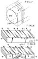
- Silicon wafers used in this invention can be prepared by slicing an ingot shown in Fig. 7 along the dash-dotted lines in accordance with the angle 0 calculated by equation (1).
- a single crystalline silicon wafer is prepared in which a surface inclined by 0 with respect to the (111) plane comprises the major surface 13 and the side surface 14 comprises the (110) plane of the crystal. Then, a plurality of parallel mask stripes 16 having a small width d are formed on the major surface 13 with a constant P as shown in Fig. 8. Thereupon, the wafer is selectively etched with the etching solution described above by using the mask stripes.
- the portions of the silicon crystal 15 between adjacent mask stripes are etched, whereupon a plurality of inverted triangular asymmetrical grooves 18 are formed, as shown in Fig. 9, each having one inner surface 17L or (111) plane inclined by 0 with respect to the major surface 13 and the other inner surface 17R or the (111) plane, the length of the base of the inverted triangular groove being substantially equal to the spacing or constant P between adjacent mask stripes 16.
- the etching process of the single crystalline silicon 15 is terminated.
- the mask stripes 16 are removed to obtain a desired planar diffraction grating provided with the plurality of inverted triangular grooves 18 in the major surface.
- a metal coat 19 comprising, for example, a nichrome layer 19a vapour deposited or sputtered and a gold layer 19b deposited on the nichrome layer by the same method.
- a gold layer is preferred because it is possible to readily obtain a percentage of reflection of higher than 95% with respect to wavelength between 7000A and 1.6 microns, especially when the diffraction grating of this invention is used as a demultiplexer for a wavelength-division-multiplexing optical fibre transmission system. If deposited directly on the grooves 18, the gold layer 19b will react with silicon to form a eutectic state.
- the lower layer 19a of nichrome which hardly reacts with gold to form a eutectic state.
- the upper layer of the coat 19 is made of such metals having the highest percentage of reflection such as gold, aluminium, etc., whereas the lower layer acts as a buffer when the upper layer is deposited thereon. It should be understood that nickel, chromium or titanium may be substituted for nichrome.
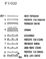
- the diffraction grating of this invention can be prepared in a manner described above. A typical example of the steps of manufacturing the diffraction grating will now be described with reference to Fig. 12.
- an etching protection film consisting of Sio 2 or Si 3 N 4 is formed on a predetermined silicon wafer (whose major surface is inclined by 0 with respect to the (111) plane) as shown in steps 1 and 2 of Fig. 12.
- a photoresist is coated on the surface of the wafer.
- a mask pattern is formed on the etching protective film by using a mask having a constant P and a stripe width of d, and exposing and developing the exposed photoresist as shown in steps 4 to 6. Windows are formed through the protective film with buffer hydrofluoric acid for the Si0 2 film and plasma etching for the Si 3 N 4 film.
- the photoresist is removed.
- the wafer formed with windows is anisotropically etched in a KOH solution to form grooves having asymmetric triangular cross-sectional configuration in the surface of the wafer.
- the etching protective film is removed.
- the percentage reflection of the silicon wafer is about 35% in a 0.8 micron wavelength region.
- a metal layer consisting of gold on nichrome, for example, is vapour deposited, at step 10.
- Another feature of this invention lies in the provision of a novel method that makes the flat portions EF, GH, IJ ... shown in Fig. 4b to become sufficiently smaller than the constant P while maintaining the stripe width d of the etching protective film at a relatively large value.
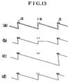
- the grooves bounded by the ⁇ 111 ⁇ planes are formed by the anisotropic etching. Thereafter, when the wafer is subjected to isotropic etching with a nitric acid-hydrofluoric acid etching solution without removing the protective film, the flat portions can be reduced sufficiently. Instead of using the isotropic etching, where the anisotropic etching is performed for a sufficiently long time, the portions can be reduced because R 111 ⁇ 0.
- the isotropic etching is more advantageous than the anisotropic etching over a long time in that the required etching time can be reduced because it is possible to make the etching speed R'111 in the direction of ⁇ 111 > at the time of the isotropic etching much larger than the etching speed Rill in the direction of ⁇ 111 > at the time of the anisotropic etching, thereby greatly reducing the required etching time. This reduces exfoliation of the protective film during etching. Moreover, in the event that the etching protective film happens to peel off, the isotropic etching is superior as evidenced by Figs. 13a to 13d. More particularly, assume now that under a state shown in Fig.
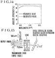
- Fig. 14 shows the result of measurement of a planar diffraction grating prepared by the method described above and having a pitch of 4 microns, and a blaze angle of 6.2°, the measurement being made for a 0.8 micron wavelength region with incident light normal to the surface of the diffraction grating.
- Fig. 14 shows the result of measurement performed on a diffraction grating prepared by using a protective film consisting of Si 3 N 4 , but substantially the same characteristic was obtained when the protective film was made of Si0 2 .
- the absolute diffraction efficiency of a commercially available diffraction grating (manufactured by Bausch & Lomb and having a 0.86 micron blaze, 300 grooves/mm, and coated with gold) was measured to be about 85% (0.7 dB in terms of loss) at a wavelength of 0.85 micron.
- This diffraction grating is said to have higher diffraction efficiency than any other commercially available diffraction gratings. Comparison of these data shows that the diffraction grating obtained by this invention has a higher efficiency than any of the prior art diffraction gratings.
- the diffraction grating structure obtained by this invention is suitable to be used as a demultiplexer for a wavelength-division-multiplexing optical fibre transmission system.
- Fig. 15 shows the construction of a Littrow mounting demultiplexer which was used in the experiment.
- Transmission fibre (input fibre) and output fibres are densely arrayed on the focal plane of a lens by using the fact that these fibres have high accuracies of their outer diameters.
- the diffraction grating used in the experiment had characteristics similar to those shown in Fig. 14.
- the focal length f of the lens can be determined by the following equation where P represents the period or constant of the diffraction grating, f3 the angle between a normal to the plane of the diffraction grating and diffracted light, and d ⁇ /dl the wavelength dispersion on the focal plane.
- P 4 microns
- dA/di can be calculated as 250A/150 microns based on the wavelength spacing (the spacing was set to be 250A in the experiment) of the channels, and the centre-to-centre distance between adjacent output fibres each having an outer diameter of 150 microns.
Landscapes
- Physics & Mathematics (AREA)
- Engineering & Computer Science (AREA)
- General Physics & Mathematics (AREA)
- Optics & Photonics (AREA)
- Manufacturing & Machinery (AREA)
- Chemical & Material Sciences (AREA)
- General Chemical & Material Sciences (AREA)
- Condensed Matter Physics & Semiconductors (AREA)
- Chemical Kinetics & Catalysis (AREA)
- Computer Hardware Design (AREA)
- Microelectronics & Electronic Packaging (AREA)
- Power Engineering (AREA)
- Diffracting Gratings Or Hologram Optical Elements (AREA)
Claims (6)
Priority Applications (1)
| Application Number | Priority Date | Filing Date | Title |
|---|---|---|---|
| DE8282100228T DE2967536D1 (en) | 1978-07-18 | 1979-07-16 | A method of manufacturing a curved diffraction grating structure |
Applications Claiming Priority (6)
| Application Number | Priority Date | Filing Date | Title |
|---|---|---|---|
| JP8734478A JPS5515133A (en) | 1978-07-18 | 1978-07-18 | Production of plane diffraction grating |
| JP87344/78 | 1978-07-18 | ||
| JP40517/79 | 1979-04-04 | ||
| JP4051779A JPS55133004A (en) | 1979-04-04 | 1979-04-04 | Production of nonplane diffraction grating |
| JP4166979A JPS5946363B2 (ja) | 1979-04-06 | 1979-04-06 | 平面回折格子の製法 |
| JP41669/79 | 1979-04-06 |
Related Child Applications (1)
| Application Number | Title | Priority Date | Filing Date |
|---|---|---|---|
| EP82100228.4 Division-Into | 1979-07-16 |
Publications (2)
| Publication Number | Publication Date |
|---|---|
| EP0007108A1 EP0007108A1 (fr) | 1980-01-23 |
| EP0007108B1 true EP0007108B1 (fr) | 1983-04-13 |
Family
ID=27290502
Family Applications (2)
| Application Number | Title | Priority Date | Filing Date |
|---|---|---|---|
| EP82100228A Expired EP0059304B1 (fr) | 1978-07-18 | 1979-07-16 | Procédé pour la réalisation d'une structure de réseau de diffraction courbe |
| EP79102442A Expired EP0007108B1 (fr) | 1978-07-18 | 1979-07-16 | Méthode de fabrication d'une structure de réseaux de diffraction |
Family Applications Before (1)
| Application Number | Title | Priority Date | Filing Date |
|---|---|---|---|
| EP82100228A Expired EP0059304B1 (fr) | 1978-07-18 | 1979-07-16 | Procédé pour la réalisation d'une structure de réseau de diffraction courbe |
Country Status (3)
| Country | Link |
|---|---|
| US (2) | US4330175A (fr) |
| EP (2) | EP0059304B1 (fr) |
| CA (1) | CA1113752A (fr) |
Families Citing this family (82)
| Publication number | Priority date | Publication date | Assignee | Title |
|---|---|---|---|---|
| US4401367A (en) * | 1980-11-03 | 1983-08-30 | United Technologies Corporation | Method for pattern masking objects and the products thereof |
| EP0058214B1 (fr) * | 1981-02-16 | 1985-06-19 | International Business Machines Corporation | Méthode pour augmenter la résistance de la surface d'un matériau solide à la gravure |
| US4357204A (en) * | 1981-06-01 | 1982-11-02 | Honeywell Inc. | Chemically machined spectral grating |
| NL8304311A (nl) * | 1983-12-15 | 1985-07-01 | Philips Nv | Reflectieraster. |
| JPS60230601A (ja) * | 1984-05-01 | 1985-11-16 | Masayasu Negishi | 膜処理方法 |
| US4729640A (en) * | 1984-10-03 | 1988-03-08 | Canon Kabushiki Kaisha | Liquid crystal light modulation device |
| DE3610333A1 (de) * | 1985-04-19 | 1986-11-27 | Siemens AG, 1000 Berlin und 8000 München | Verfahren zur herstellung eines oberflaechengitters mit einer bestimmten gitterkonstanten auf einem tieferliegenden oberflaechenbereich einer mesastruktur |
| US4758090A (en) * | 1986-09-25 | 1988-07-19 | Allied-Signal Inc. | Optical wavelength monitor using blazed diffraction grating |
| EP0286855A1 (fr) * | 1987-04-15 | 1988-10-19 | BBC Brown Boveri AG | Procédé pour creuser des sillons dans un substrat de silicium |
| US5004673A (en) * | 1987-04-20 | 1991-04-02 | Environmental Research Institute Of Michigan | Method of manufacturing surface relief patterns of variable cross-sectional geometry |
| DE3852296T2 (de) * | 1988-03-18 | 1995-04-13 | Instruments Sa | Beugungsgitter und Herstellungsverfahren dafür. |
| JPH0833527B2 (ja) * | 1988-07-18 | 1996-03-29 | キヤノン株式会社 | 光学的ローパスフィルターを有した撮影系 |
| EP0387407B1 (fr) * | 1989-02-23 | 1993-09-08 | Landis & Gyr Business Support AG | Réseau de diffraction |
| US5283690A (en) * | 1989-04-04 | 1994-02-01 | Sharp Kabushiki Kaisha | Optical diffraction grating element |
| US5035770A (en) * | 1989-05-01 | 1991-07-30 | Hewlett-Packard Company | Methods of making surface relief gratings |
| GB8919220D0 (en) * | 1989-08-24 | 1989-10-04 | British Telecomm | Diffraction grating assembly |
| DE4111783C1 (fr) * | 1991-04-11 | 1992-05-27 | Ant Nachrichtentechnik Gmbh, 7150 Backnang, De | |
| US5116461A (en) * | 1991-04-22 | 1992-05-26 | Motorola, Inc. | Method for fabricating an angled diffraction grating |
| JP2524568B2 (ja) * | 1991-09-18 | 1996-08-14 | キヤノン株式会社 | カラ―画像読取装置 |
| DE4206677C1 (fr) * | 1992-02-28 | 1993-09-02 | Siemens Ag, 80333 Muenchen, De | |
| US6776094B1 (en) * | 1993-10-04 | 2004-08-17 | President & Fellows Of Harvard College | Kit For Microcontact Printing |
| US6180239B1 (en) | 1993-10-04 | 2001-01-30 | President And Fellows Of Harvard College | Microcontact printing on surfaces and derivative articles |
| US5776748A (en) | 1993-10-04 | 1998-07-07 | President And Fellows Of Harvard College | Method of formation of microstamped patterns on plates for adhesion of cells and other biological materials, devices and uses therefor |
| US5900160A (en) * | 1993-10-04 | 1999-05-04 | President And Fellows Of Harvard College | Methods of etching articles via microcontact printing |
| EP0676614B1 (fr) * | 1994-04-11 | 2001-06-20 | International Business Machines Corporation | Calibrages standards pour profilomètre et méthode de sa production |
| US5907436A (en) * | 1995-09-29 | 1999-05-25 | The Regents Of The University Of California | Multilayer dielectric diffraction gratings |
| JP3270814B2 (ja) * | 1996-08-27 | 2002-04-02 | 日本板硝子株式会社 | 回折型光学素子の製造方法 |
| US6020047A (en) * | 1996-09-04 | 2000-02-01 | Kimberly-Clark Worldwide, Inc. | Polymer films having a printed self-assembling monolayer |
| US6048623A (en) * | 1996-12-18 | 2000-04-11 | Kimberly-Clark Worldwide, Inc. | Method of contact printing on gold coated films |
| US6480333B1 (en) * | 1997-11-19 | 2002-11-12 | California Institute Of Technology | Diffractive optical elements on non-flat substrates using electron beam lithography |
| JP3559710B2 (ja) * | 1998-05-25 | 2004-09-02 | キヤノン株式会社 | 回折光学素子及びそれを用いた走査光学装置 |
| AU3763800A (en) * | 1999-03-22 | 2000-10-09 | Mems Optical, Inc. | Diffractive selectively polarizing beam splitter and beam routing prisms produced thereby |
| DE19937023A1 (de) * | 1999-08-05 | 2001-02-08 | Heidenhain Gmbh Dr Johannes | Reflexions-Maßverkörperung und Verfahren zur Herstellung einer Reflexions-Maßverkörperung |
| EP1203243A1 (fr) * | 1999-08-11 | 2002-05-08 | IMOS Gubela GmbH | Dispositif de barriere lumineuse a separateur de faisceau |
| AU1926601A (en) * | 1999-11-22 | 2001-06-04 | California Institute Of Technology | Micro photonic particle sensor |
| US6400509B1 (en) * | 2000-04-07 | 2002-06-04 | Zolo Technologies, Inc. | Apparatus and method for the reduction of polarization sensitivity in diffraction gratings used in fiber optic communications devices |
| US6517734B1 (en) * | 2000-07-13 | 2003-02-11 | Network Photonics, Inc. | Grating fabrication process using combined crystalline-dependent and crystalline-independent etching |
| US6449096B1 (en) * | 2000-07-13 | 2002-09-10 | Network Photonics, Inc. | Diffraction grating with reduced polarization-dependent loss |
| JP2002098820A (ja) | 2000-09-21 | 2002-04-05 | Nippon Sheet Glass Co Ltd | 反射型回折格子 |
| FR2815933B1 (fr) * | 2000-10-26 | 2003-01-24 | Eads Airbus Sa | Organe et dispositif de transmission d'efforts radiaux entre des regions centrale et d'extremite de cet organe |
| US6657723B2 (en) * | 2000-12-13 | 2003-12-02 | International Business Machines Corporation | Multimode planar spectrographs for wavelength demultiplexing and methods of fabrication |
| WO2002071119A1 (fr) * | 2001-03-01 | 2002-09-12 | Zolo Technologies, Inc. | Multiplexeur/demultiplexeur presentant une configuration a quatre f' et lentille hybride |
| US6608712B2 (en) | 2001-05-15 | 2003-08-19 | Network Photonics, Inc. | Hidden flexure ultra planar optical routing element |
| US6583933B2 (en) | 2001-05-16 | 2003-06-24 | The Regents Of The University Of California | Reflective diffraction grating |
| US6614581B2 (en) | 2001-07-03 | 2003-09-02 | Network Photonics, Inc. | Methods and apparatus for providing a multi-stop micromirror |
| US6625342B2 (en) * | 2001-07-03 | 2003-09-23 | Network Photonics, Inc. | Systems and methods for overcoming stiction using a lever |
| US7223368B2 (en) * | 2002-05-03 | 2007-05-29 | Kimberly-Clark Worldwide, Inc. | Diffraction-based diagnostic devices |
| US7223534B2 (en) * | 2002-05-03 | 2007-05-29 | Kimberly-Clark Worldwide, Inc. | Diffraction-based diagnostic devices |
| US7485453B2 (en) | 2002-05-03 | 2009-02-03 | Kimberly-Clark Worldwide, Inc. | Diffraction-based diagnostic devices |
| US7771922B2 (en) * | 2002-05-03 | 2010-08-10 | Kimberly-Clark Worldwide, Inc. | Biomolecule diagnostic device |
| US7118855B2 (en) | 2002-05-03 | 2006-10-10 | Kimberly-Clark Worldwide, Inc. | Diffraction-based diagnostic devices |
| US7214530B2 (en) | 2002-05-03 | 2007-05-08 | Kimberly-Clark Worldwide, Inc. | Biomolecule diagnostic devices and method for producing biomolecule diagnostic devices |
| US6785039B2 (en) | 2002-06-03 | 2004-08-31 | Pts Corporation | Optical routing elements |
| US7091049B2 (en) * | 2002-06-26 | 2006-08-15 | Kimberly-Clark Worldwide, Inc. | Enhanced diffraction-based biosensor devices |
| JP2004045672A (ja) * | 2002-07-11 | 2004-02-12 | Canon Inc | 偏光分離素子およびそれを用いた光学系 |
| US7169550B2 (en) | 2002-09-26 | 2007-01-30 | Kimberly-Clark Worldwide, Inc. | Diffraction-based diagnostic devices |
| US20060204185A1 (en) * | 2005-03-09 | 2006-09-14 | Konica Minolta Holdings, Inc. | Diffractive optical element and bidirectional optical communication module using the same |
| RU2009108311A (ru) * | 2006-08-09 | 2010-09-20 | Конинклейке Филипс Электроникс Н.В. (Nl) | Светоизлучающее устройство, в частности, для измерения потока |
| DE102007011560A1 (de) * | 2007-03-02 | 2008-09-04 | Seereal Technologies S.A. | Vorrichtung zur Minimierung der verbeugungsbedingten Dispersion in Lichtmodulatoren |
| US8958070B2 (en) * | 2007-05-29 | 2015-02-17 | OptoTrace (SuZhou) Technologies, Inc. | Multi-layer variable micro structure for sensing substance |
| AU2010240706B2 (en) * | 2009-04-20 | 2013-07-25 | Snap Inc. | Improvements in optical waveguides |
| US10642039B2 (en) * | 2009-04-20 | 2020-05-05 | Bae Systems Plc | Surface relief grating in an optical waveguide having a reflecting surface and dielectric layer conforming to the surface |
| CN101900844B (zh) * | 2010-05-07 | 2012-01-04 | 上海理工大学 | 闪耀凸面光栅的反应离子束蚀刻方法 |
| US20120021555A1 (en) * | 2010-07-23 | 2012-01-26 | Taiwan Semiconductor Manufacturing Company, Ltd. | Photovoltaic cell texturization |
| CN102667317B (zh) * | 2010-07-30 | 2014-11-26 | 索尼公司 | 照明单元和显示装置 |
| US11079543B1 (en) * | 2010-09-23 | 2021-08-03 | Lawrence Livermore National Security, Llc | Isotropic etchback method of linewidth tailoring multilayer dielectric diffraction gratings for improvement of laser damage resistance and diffraction efficiency |
| JP5864920B2 (ja) * | 2010-12-20 | 2016-02-17 | キヤノン株式会社 | 回折格子の製造方法 |
| US8970956B2 (en) * | 2011-03-30 | 2015-03-03 | Intel Corporation | On-chip diffraction grating prepared by crystallographic wet-etch |
| EP2533077A1 (fr) * | 2011-06-08 | 2012-12-12 | Nederlandse Organisatie voor toegepast -natuurwetenschappelijk onderzoek TNO | Réseau de diffraction et son procédé de production |
| TWI458122B (zh) * | 2011-11-23 | 2014-10-21 | Toshiba Kk | 半導體發光元件 |
| TWI440833B (zh) * | 2011-12-30 | 2014-06-11 | Oto Photonics Inc | 混合式繞射光柵、模具及繞射光柵及其模具的製造方法 |
| JP6058402B2 (ja) * | 2012-06-08 | 2017-01-11 | 株式会社日立ハイテクノロジーズ | 曲面回折格子の製造方法、および曲面回折格子の型 |
| JP6049320B2 (ja) * | 2012-06-20 | 2016-12-21 | キヤノン株式会社 | 回折格子および回折格子の製造方法 |
| JP6029502B2 (ja) | 2013-03-19 | 2016-11-24 | 株式会社日立ハイテクノロジーズ | 曲面回折格子の製造方法 |
| WO2016059928A1 (fr) * | 2014-10-16 | 2016-04-21 | 株式会社 日立ハイテクノロジーズ | Procédé de fabrication de moule pour réseau de diffraction incurvé, procédé de fabrication de réseau de diffraction incurvé, réseau de diffraction incurvé, et dispositif optique |
| US10900832B2 (en) * | 2016-06-06 | 2021-01-26 | Shimadzu Corporation | Diffraction grating and spectral device |
| TWI715599B (zh) | 2016-07-12 | 2021-01-11 | 台灣超微光學股份有限公司 | 光譜儀模組及其製作方法 |
| US11391871B2 (en) * | 2017-12-27 | 2022-07-19 | Hitachi High-Tech Corporation | Manufacturing method of concave diffraction grating, concave diffraction grating, and analyzer using the same |
| US10302826B1 (en) | 2018-05-30 | 2019-05-28 | Applied Materials, Inc. | Controlling etch angles by substrate rotation in angled etch tools |
| CN113039627A (zh) | 2018-11-07 | 2021-06-25 | 应用材料公司 | 呈角度的光栅的形成 |
| JP7417611B2 (ja) | 2018-12-17 | 2024-01-18 | アプライド マテリアルズ インコーポレイテッド | 傾斜回折格子のローリングkベクトルの調整 |
| CN109932769B (zh) * | 2019-03-29 | 2022-07-05 | 北京至格科技有限公司 | 光栅的刻蚀控制方法及装置 |
Family Cites Families (9)
| Publication number | Priority date | Publication date | Assignee | Title |
|---|---|---|---|---|
| DE810414C (de) * | 1948-10-02 | 1951-08-09 | Doris Dr Kuhlmann | Verfahren zur Herstellung von Roentgenreflektoren |
| US3334959A (en) * | 1963-10-17 | 1967-08-08 | Bell Telephone Labor Inc | Adjustable optical device |
| US3697369A (en) * | 1964-12-04 | 1972-10-10 | Owens Illinois Inc | Plastic lined receptacle or the like |
| US3443243A (en) * | 1965-06-23 | 1969-05-06 | Bell Telephone Labor Inc | Frequency selective laser |
| US3521943A (en) * | 1966-09-30 | 1970-07-28 | Herman F Kelderman | Apparatus for generating aspheric reflecting surfaces useful for correcting spherical aberration |
| US3530010A (en) * | 1968-07-22 | 1970-09-22 | Research Corp | Method of making blazed optical diffraction gratings |
| US3654012A (en) * | 1970-02-04 | 1972-04-04 | Uniroyal Inc | Method of making a composite plastic article of manufacture |
| US3777156A (en) * | 1972-02-14 | 1973-12-04 | Hewlett Packard Co | Bent diffraction crystal with geometrical aberration compensation |
| US4357204A (en) * | 1981-06-01 | 1982-11-02 | Honeywell Inc. | Chemically machined spectral grating |
-
1979
- 1979-07-16 EP EP82100228A patent/EP0059304B1/fr not_active Expired
- 1979-07-16 EP EP79102442A patent/EP0007108B1/fr not_active Expired
- 1979-07-17 CA CA331,934A patent/CA1113752A/fr not_active Expired
- 1979-07-17 US US06/058,382 patent/US4330175A/en not_active Expired - Lifetime
-
1981
- 1981-11-30 US US06/325,721 patent/US4405405A/en not_active Expired - Lifetime
Also Published As
| Publication number | Publication date |
|---|---|
| EP0007108A1 (fr) | 1980-01-23 |
| US4405405A (en) | 1983-09-20 |
| US4330175A (en) | 1982-05-18 |
| EP0059304A2 (fr) | 1982-09-08 |
| EP0059304A3 (en) | 1982-11-10 |
| CA1113752A (fr) | 1981-12-08 |
| EP0059304B1 (fr) | 1985-10-23 |
Similar Documents
| Publication | Publication Date | Title |
|---|---|---|
| EP0007108B1 (fr) | Méthode de fabrication d'une structure de réseaux de diffraction | |
| US4512638A (en) | Wire grid polarizer | |
| US4524127A (en) | Method of fabricating a silicon lens array | |
| US7534636B2 (en) | Lids for wafer-scale optoelectronic packages | |
| JP4349104B2 (ja) | ブレーズド・ホログラフィック・グレーティング、その製造方法、及びレプリカグレーティング | |
| US11747529B2 (en) | Wafer level microstructures for an optical lens | |
| JP2565094B2 (ja) | 光結合構造 | |
| US4885055A (en) | Layered devices having surface curvature and method of constructing same | |
| US6517734B1 (en) | Grating fabrication process using combined crystalline-dependent and crystalline-independent etching | |
| US7267781B2 (en) | Method of fabricating optical filters | |
| US20080038660A1 (en) | Method Of Making Grating Structures Having High Aspect Ratio | |
| EP1219991B1 (fr) | Terminaison de ruban de fibres optiques conservant la polarisation | |
| US7267780B1 (en) | Formation of facets on optical components | |
| GB2099373A (en) | Manufacture of diffraction gratings | |
| JPS62145208A (ja) | 導波路回折格子の製造方法 | |
| JPS5946363B2 (ja) | 平面回折格子の製法 | |
| von Lingelsheim et al. | Fabrication of micro-optical wavelength division multiplexer (WDM) gratings on glass using an ion etching technique | |
| JP2663841B2 (ja) | 光結合構造の製造方法 | |
| JPS6314321B2 (fr) | ||
| EP0490320A2 (fr) | Méthode pour la production d'un réseau de diffraction | |
| JPS5891407A (ja) | シリコン回折格子の製造方法 | |
| KR100291555B1 (ko) | 기판 식각 장치 및 이를 이용한 실리콘 맴브레인 제조 방법 | |
| JPS6242103A (ja) | ブレ−ズ格子の製造方法 | |
| JPS58117511A (ja) | 回折格子 | |
| JPH11218635A (ja) | 光ファイバアレイ用v溝基板 |
Legal Events
| Date | Code | Title | Description |
|---|---|---|---|
| PUAI | Public reference made under article 153(3) epc to a published international application that has entered the european phase |
Free format text: ORIGINAL CODE: 0009012 |
|
| AK | Designated contracting states |
Designated state(s): DE FR GB IT NL |
|
| 17P | Request for examination filed | ||
| ITF | It: translation for a ep patent filed | ||
| GRAA | (expected) grant |
Free format text: ORIGINAL CODE: 0009210 |
|
| AK | Designated contracting states |
Designated state(s): DE FR GB IT NL |
|
| REF | Corresponds to: |
Ref document number: 2965192 Country of ref document: DE Date of ref document: 19830519 |
|
| ET | Fr: translation filed | ||
| ITPR | It: changes in ownership of a european patent |
Owner name: CESSIONE;NIPPON TELEGRAPH AND TELEPHONE CORPORATIO |
|
| REG | Reference to a national code |
Ref country code: FR Ref legal event code: TP |
|
| NLS | Nl: assignments of ep-patents |
Owner name: NIPPON TELEGRAPH AND TELEPHONE CORPORATION TE TOKI |
|
| ITTA | It: last paid annual fee | ||
| REG | Reference to a national code |
Ref country code: FR Ref legal event code: CA |
|
| PGFP | Annual fee paid to national office [announced via postgrant information from national office to epo] |
Ref country code: GB Payment date: 19980624 Year of fee payment: 20 |
|
| PGFP | Annual fee paid to national office [announced via postgrant information from national office to epo] |
Ref country code: FR Payment date: 19980708 Year of fee payment: 20 |
|
| PGFP | Annual fee paid to national office [announced via postgrant information from national office to epo] |
Ref country code: NL Payment date: 19980730 Year of fee payment: 20 |
|
| PGFP | Annual fee paid to national office [announced via postgrant information from national office to epo] |
Ref country code: DE Payment date: 19980929 Year of fee payment: 20 |
|
| PG25 | Lapsed in a contracting state [announced via postgrant information from national office to epo] |
Ref country code: GB Free format text: LAPSE BECAUSE OF NON-PAYMENT OF DUE FEES Effective date: 19990715 |
|
| PG25 | Lapsed in a contracting state [announced via postgrant information from national office to epo] |
Ref country code: NL Free format text: LAPSE BECAUSE OF EXPIRATION OF PROTECTION Effective date: 19990716 |
|
| REG | Reference to a national code |
Ref country code: GB Ref legal event code: PE20 Effective date: 19990715 |
|
| NLV7 | Nl: ceased due to reaching the maximum lifetime of a patent |
Effective date: 19990716 |
|
| PLBE | No opposition filed within time limit |
Free format text: ORIGINAL CODE: 0009261 |
|
| STAA | Information on the status of an ep patent application or granted ep patent |
Free format text: STATUS: NO OPPOSITION FILED WITHIN TIME LIMIT |