EP0002102B1 - Xerographische Druck-/Kopiervorrichtung mit Mitteln zum Umwandeln der in einem latenten Bild eines Dokuments enthaltenen Information in elektrische Signale - Google Patents
Xerographische Druck-/Kopiervorrichtung mit Mitteln zum Umwandeln der in einem latenten Bild eines Dokuments enthaltenen Information in elektrische Signale Download PDFInfo
- Publication number
- EP0002102B1 EP0002102B1 EP78300439A EP78300439A EP0002102B1 EP 0002102 B1 EP0002102 B1 EP 0002102B1 EP 78300439 A EP78300439 A EP 78300439A EP 78300439 A EP78300439 A EP 78300439A EP 0002102 B1 EP0002102 B1 EP 0002102B1
- Authority
- EP
- European Patent Office
- Prior art keywords
- latent image
- electrode
- copier
- xerographic printer
- electrical signals
- Prior art date
- Legal status (The legal status is an assumption and is not a legal conclusion. Google has not performed a legal analysis and makes no representation as to the accuracy of the status listed.)
- Expired
Links
- 238000003384 imaging method Methods 0.000 claims description 5
- 238000001514 detection method Methods 0.000 description 6
- 238000000034 method Methods 0.000 description 6
- 239000002800 charge carrier Substances 0.000 description 3
- 230000000694 effects Effects 0.000 description 3
- 238000010894 electron beam technology Methods 0.000 description 3
- 238000013459 approach Methods 0.000 description 2
- 230000015572 biosynthetic process Effects 0.000 description 2
- 239000003990 capacitor Substances 0.000 description 2
- 238000003860 storage Methods 0.000 description 2
- 230000002745 absorbent Effects 0.000 description 1
- 239000002250 absorbent Substances 0.000 description 1
- 238000007792 addition Methods 0.000 description 1
- 230000005540 biological transmission Effects 0.000 description 1
- 238000013016 damping Methods 0.000 description 1
- 230000005284 excitation Effects 0.000 description 1
- 231100000206 health hazard Toxicity 0.000 description 1
- 238000004519 manufacturing process Methods 0.000 description 1
- 230000003287 optical effect Effects 0.000 description 1
- 239000002245 particle Substances 0.000 description 1
- 230000000007 visual effect Effects 0.000 description 1
Images


Classifications
-
- G—PHYSICS
- G03—PHOTOGRAPHY; CINEMATOGRAPHY; ANALOGOUS TECHNIQUES USING WAVES OTHER THAN OPTICAL WAVES; ELECTROGRAPHY; HOLOGRAPHY
- G03G—ELECTROGRAPHY; ELECTROPHOTOGRAPHY; MAGNETOGRAPHY
- G03G15/00—Apparatus for electrographic processes using a charge pattern
- G03G15/22—Apparatus for electrographic processes using a charge pattern involving the combination of more than one step according to groups G03G13/02 - G03G13/20
- G03G15/221—Machines other than electrographic copiers, e.g. electrophotographic cameras, electrostatic typewriters
-
- G—PHYSICS
- G03—PHOTOGRAPHY; CINEMATOGRAPHY; ANALOGOUS TECHNIQUES USING WAVES OTHER THAN OPTICAL WAVES; ELECTROGRAPHY; HOLOGRAPHY
- G03G—ELECTROGRAPHY; ELECTROPHOTOGRAPHY; MAGNETOGRAPHY
- G03G15/00—Apparatus for electrographic processes using a charge pattern
- G03G15/04—Apparatus for electrographic processes using a charge pattern for exposing, i.e. imagewise exposure by optically projecting the original image on a photoconductive recording material
- G03G15/04036—Details of illuminating systems, e.g. lamps, reflectors
- G03G15/04045—Details of illuminating systems, e.g. lamps, reflectors for exposing image information provided otherwise than by directly projecting the original image onto the photoconductive recording material, e.g. digital copiers
- G03G15/04072—Details of illuminating systems, e.g. lamps, reflectors for exposing image information provided otherwise than by directly projecting the original image onto the photoconductive recording material, e.g. digital copiers by laser
-
- H—ELECTRICITY
- H04—ELECTRIC COMMUNICATION TECHNIQUE
- H04N—PICTORIAL COMMUNICATION, e.g. TELEVISION
- H04N1/00—Scanning, transmission or reproduction of documents or the like, e.g. facsimile transmission; Details thereof
- H04N1/024—Details of scanning heads ; Means for illuminating the original
- H04N1/028—Details of scanning heads ; Means for illuminating the original for picture information pick-up
Definitions
- the present invention relates to xerographic printer/copier devices and is in particular directed to such a device when adapted to sense latent xerographic images of original documents to produce coded electrical signals.
- German Auslegeschrift No. 2209598 also shows an arrangement for providing signals representing the content of a latent image in a copying machine.
- This arrangement employs a copy station, a print station and an electrometer pick up device which registers the charges on the imaging element. It has the disadvantage that the generated signals are of low amplitude and are, therefore, subject to error, especially in the electrically noisy environment of a copier.
- a xerographic printer/copier device including a converter for converting information from a latent image of an original document into electrical signals comprising a photoconductive imaging element having a surface movable along a closed path past a plurality of processing stations including a charging station, a copying station operable to expose the surface, when charged, to an image of an original document to form a latent image thereon, and a printing station operable to expose the surface, when charged, to a modulated light beam scanned across the surface along a fixed line position orthogonal to the direction of movement thereof to form a latent image on the surface corresponding to modulation of the beam, characterised by a sense electrode positioned at the printing station and extending across the surface adjacent said line position and spaced from the surface such as to sense changes of charge on the surface whereby, when a latent image produced by the copying station is discharged by scanning by the light beam, when unmodulated, electrical signals corresponding to the content of the latent image are induced in the electrode,
- Fig. 1 there is shown a simplified schematic representation of a xerographic printer/copier.
- a document 2 from which an image is projected onto a photoconductor surface 4 via reflected light at an exposure station 6.
- a corona cloud from a wire maintained at high voltage at charging station 22.
- the resulting image is in the form of a charge pattern on the photoconductor surface 4 which is contiguous with rotating drum 8.
- Drum 8 rotates in the direction of arrow 10.
- the charge pattern corresponding to the document image is developed with toner at station 12.
- the toned image is then transferred to the surface of a recording medium such as paper 14 at image transfer station 16 and is fused onto the paper 14 by rollers 18.
- the scanning laser 24 and its optical system is added.
- a scanned and modulated laser beam 26 is scanned on the photoconductor surface 4 adjacent to toner station 12 in order to discharge the photoconductor surface, previously uniformly charged at station 22, and thereby form a charged image thereon.
- the image is toned and transferred to a recording surface such as paper.
- a charge pattern image is formed from a document 2 on the photoconductor 4 as indicated above.
- the image is scanned by laser beam 26.
- Laser beam 26 is generated from laser 24, is passed through modulator 25 and is scanned across drum 8 by rotating mirror segments 28 via lens 27.
- the current discharged from the photoconductor 4 induces a current on a sense electrode 30, which is amplified.
- the amplified current is modified by the compensation circuit 32 then converted to a coded signal at codifier 34.
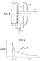
- Fig. 3 depicts the present system in detail. There is shown sense electrode 30 together with compensation circuit 32. Adjacent to electrode 30 is shield 35 which is used to minimize noise that is present in the environment of the drum.
- a cross section of photoconductor 4 shows that the photoconductor 4 has both a charge generation layer 3 and a charge transport layer 5, as is common with photocopiers employing organic photoconductors.
- the photoconductor surface 4 is charged at 22 by a corona wire maintained at a high voltage.
- the charged photoconductor 4 is exposed, as in a conventional photocopier (see Fig. 1), to light reflected from an image of the object to be copied.
- the result is a surface charge or potential image on the photoconductor 4 which corresponds to an image of the object.
- This surface charge is detected and stored electronically in the following manner.
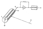
- a laser beam 26 (6328 A, for example) is scanned across the surface of the photmconductor 4 as the photoconductor 4 is moved slowly in a direction perpendicular to the direction of scan.
- This laser scan system is represented schematically in Fig. 2.
- the small spot of laser light which is scanned impinging on the surface of the photoconductor causes the surface charge to be neutralized.
- the surface potential at the scanned spot changes from the initial charged value to zero.
- the change in surface potential is detected by a sense electrode 30 near the photoconductor surface along the path of the scanned light spot, and converted into a coded electronic signal suitable for facsimile transmission or for storage in a computer memory/storage.
- Fig. 3 displays schematically a cross- section of the photoconductor and the detection electrode.
- the peak of the current pulse produced by the discharge of one picture element of dimension 1 2 is i P , where and where
- the induced current is high enough to permit detection by a conventional low impedance video amplifier.
- the signal current measured in practice may vary considerably from the above.
- Noise in the image detection system can be classified into a few dominant categories: microphonic noise due to vibration of the electrode, noise in the laser light source, and leakage electromagnetic interference (EMI) from the corona wire used in the photocopier.
- the microphonic noise can be minimized by standard vibration damping techniques.
- EMI noise, particularly that generated by the corona wire, can be minimized by shielding the detector electrode 30 with shield 35 and input circuitry.
- Laser noise depends upon the type and age of the laser and its power supply.
- a difficulty with the laser discharge method of detection arises because of the complex time response of the photoconductor.
- the instantaneous excitation of charge results in an induced current which extends over a finite period of time.
- the two components of the time response, fast and slow, are determined by the transit time and the trapping and re-release of charge, respectively, for charge carriers in the charge transport layer 3.
- the induced current produced by scanning the laser across a negligibly small spot of charge is represented in Fig. 4.
- Each spot of charge which is discharged by the scanned laser induces a similar component of current, all of which add up to the total measured current.
- the induced current in the ideal case represented in Fig. 4 rises rapidly to a maximum value and then decays exponentially with the fast time constant T , which is due to the finite transit time of the charge carriers.
- T fast time constant
- a large background current due to the straggling of charge carriers decays more slowly, with a time constant Tl .
- Tl time constant
- the transit time T is comparable to the time required to scan one picture element, while the time Tl , is much longer.
- the effect of the finite decay times T and TI is to blur the images detected by this technique.
- a technique for improving the detected image by removing the blurring of the image involves the use of an electronic compensation circuit.
- One example of such a circuit is shown in Fig. 5.
- the operation of the circuit in Fig. 5 is outlined by the sequence of signals shown in Figs. 6, 7 and 8.
- a pulse of light is applied to a charged area of the photoconductor, as is represented in Fig. 6.
- the discharge of the photoconductor surface induces a current in the sense electrode 30, which is detected as a voltage V, (Fig. 7).
- the voltage V I which decays with both a fast component T and a slow component T ,, is equal to the induced current multiplied by R 1 .
- the amplifiers A 1 , A 2 and A 3 are high gain, wide band operational amplifiers.
- the voltage V I is typically where A and B are determined by characteristics of the photoconductor, and t is time.
- the output voltage V 2 (Fig. 8) from the compensation circuit is where S represents the transfer function of the amplifiers.
- resistors and capacitors are adjusted so that, and
- the resistors may all be chosen to be a common value such as 10 K ⁇ so that the capacitors C,, C 2 , and C 3 are determined from the equations supra.
- the output of the compensation circuit is V 2 , which shows no effect of the blurring due to the finite decay times T and T1' as is illustrated in Fig. 8.
- Fig. 9 An alternative scheme for eliminating the effect of the finite response time of the photoconductor is outlined in Fig. 9.
- the scanned laser light beam 26 is chopped at a fixed frequency, and the resulting current measured on the sense electrode 30 is amplified and filtered to detect signals at the chopping frequency.
- the output of the electrode does not exhibit the blurring of the detected image which is normally caused by the finite response time of the photoconductor.
- it is important that the chopping frequency is higher than the highest frequency in the detected signal.
- One scheme for accomplishing the chopping of the scanned laser light involves passing the scanning laser beam through a slotted aperture 36 which is in proximity to the sense electrode structure, as is illustrated in Fig. 9.
Landscapes
- Physics & Mathematics (AREA)
- General Physics & Mathematics (AREA)
- Engineering & Computer Science (AREA)
- Multimedia (AREA)
- Signal Processing (AREA)
- Optics & Photonics (AREA)
- Exposure Or Original Feeding In Electrophotography (AREA)
- Dot-Matrix Printers And Others (AREA)
- Laser Beam Printer (AREA)
- Mechanical Optical Scanning Systems (AREA)
Claims (5)
Applications Claiming Priority (2)
| Application Number | Priority Date | Filing Date | Title |
|---|---|---|---|
| US852394 | 1977-11-17 | ||
| US05/852,394 US4204725A (en) | 1977-11-17 | 1977-11-17 | Apparatus for detecting information stored on photocopying media, transmitting and storing the same |
Publications (2)
| Publication Number | Publication Date |
|---|---|
| EP0002102A1 EP0002102A1 (de) | 1979-05-30 |
| EP0002102B1 true EP0002102B1 (de) | 1982-09-08 |
Family
ID=25313193
Family Applications (1)
| Application Number | Title | Priority Date | Filing Date |
|---|---|---|---|
| EP78300439A Expired EP0002102B1 (de) | 1977-11-17 | 1978-10-02 | Xerographische Druck-/Kopiervorrichtung mit Mitteln zum Umwandeln der in einem latenten Bild eines Dokuments enthaltenen Information in elektrische Signale |
Country Status (8)
| Country | Link |
|---|---|
| US (1) | US4204725A (de) |
| EP (1) | EP0002102B1 (de) |
| JP (1) | JPS54105552A (de) |
| AR (1) | AR223825A1 (de) |
| BR (1) | BR7807553A (de) |
| CA (1) | CA1114006A (de) |
| DE (1) | DE2862025D1 (de) |
| IT (1) | IT1160060B (de) |
Families Citing this family (29)
| Publication number | Priority date | Publication date | Assignee | Title |
|---|---|---|---|---|
| US4777102A (en) * | 1976-08-27 | 1988-10-11 | Levine Alfred B | Method and apparatus for electronic development of color photographic film |
| US4745040A (en) * | 1976-08-27 | 1988-05-17 | Levine Alfred B | Method for destructive electronic development of photo film |
| JPS5598719A (en) * | 1979-01-20 | 1980-07-28 | Canon Inc | High speed scanner |
| JPS5664354A (en) * | 1979-10-30 | 1981-06-01 | Canon Inc | Copying method and device |
| US4326796A (en) * | 1979-12-13 | 1982-04-27 | International Business Machines Corporation | Apparatus and method for measuring and maintaining copy quality in an electrophotographic copier |
| US4294534A (en) * | 1980-01-14 | 1981-10-13 | Xerox Corporation | Multiple function reproduction apparatus |
| US4345835A (en) * | 1980-01-14 | 1982-08-24 | Xerox Corporation | Multiple function reproduction apparatus |
| DE3173408D1 (en) * | 1980-01-14 | 1986-02-20 | Xerox Corp | Copying apparatus |
| JPS56100563A (en) * | 1980-01-14 | 1981-08-12 | Konishiroku Photo Ind Co Ltd | Information composite recording device |
| US4332463A (en) * | 1980-06-20 | 1982-06-01 | Eastman Kodak Company | Non-synchronous operation of an electronic copier |
| US4348100A (en) * | 1980-09-02 | 1982-09-07 | Xerox Corporation | Control for xerographic system |
| US4371897A (en) * | 1980-09-02 | 1983-02-01 | Xerox Corporation | Fluorescent activated, spatially quantitative light detector |
| JPS57154973A (en) * | 1981-03-19 | 1982-09-24 | Minolta Camera Co Ltd | Controller of electrostatic recorder |
| US4624543A (en) * | 1981-08-26 | 1986-11-25 | Savin Corporation | Method and apparatus for electrophotographically processing information |
| JPS5842068A (ja) * | 1981-09-07 | 1983-03-11 | Hitachi Ltd | 画像読取装置 |
| US4632538A (en) * | 1984-10-25 | 1986-12-30 | Lemelson Jerome H | Video terminal and printer |
| GB2184315A (en) * | 1985-12-17 | 1987-06-17 | Spence Bate | Reading electric charge images |
| JPS62201470A (ja) * | 1986-02-28 | 1987-09-05 | Minolta Camera Co Ltd | 電子写真複写機制御方法 |
| GB8610494D0 (en) * | 1986-04-29 | 1986-06-04 | Univ Manchester | Images |
| US4693593A (en) * | 1986-06-24 | 1987-09-15 | Eastman Kodak Company | Electrographic process control |
| DE3783984T2 (de) * | 1986-09-16 | 1993-05-19 | Matsushita Electric Ind Co Ltd | Kopierer mit positionskontrollierbarer subabtasteinrichtung. |
| US4884857A (en) * | 1987-11-09 | 1989-12-05 | International Business Machines Corporation | Scanner for use in multiple spot laser electrophotographic printer |
| CA1276320C (en) * | 1987-12-01 | 1990-11-13 | John Allan Rowlands | System for measuring the charge distribution on a photoreceptor surface |
| US4967238A (en) * | 1988-12-22 | 1990-10-30 | Xerox Corporation | Cleaning performance monitor |
| US5097350A (en) * | 1990-06-06 | 1992-03-17 | Interfax, Inc. | Method and apparatus for adapting an electrostatic copier machine to a plain paper facsimile transceiver |
| US5113082A (en) * | 1990-09-11 | 1992-05-12 | Moshe Golberstein | Electro-optical instrument with self-contained photometer |
| US5125013A (en) * | 1991-08-08 | 1992-06-23 | Eastman Kodak Company | Method of scanning of toned image in a liquid gate |
| EP1680911A1 (de) * | 2003-11-05 | 2006-07-19 | Siemens Aktiengesellschaft | Scanner/kopierer basierend auf organischen materialien |
| US7403214B2 (en) * | 2006-02-21 | 2008-07-22 | Lexmark International, Inc. | Systems and methods for adjusting the dynamic range of a scanning laser beam |
Family Cites Families (11)
| Publication number | Priority date | Publication date | Assignee | Title |
|---|---|---|---|---|
| US3050580A (en) * | 1957-02-04 | 1962-08-21 | Xerox Corp | Electrostatic techniques |
| GB964882A (en) * | 1960-05-17 | 1964-07-22 | Gevaert Photo Prod Nv | Improvements in or relating to electrostatic recording |
| US3681527A (en) * | 1968-03-15 | 1972-08-01 | Hitachi Ltd | Facsimile reading and recording device |
| US3660818A (en) * | 1970-05-04 | 1972-05-02 | Rca Corp | Electro-optical memory |
| US4042962A (en) * | 1971-03-01 | 1977-08-16 | Canon Kabushiki Kaisha | Composite information operating method and apparatus |
| US3898001A (en) * | 1973-08-14 | 1975-08-05 | Xerox Corp | Electrometer system for non-contact detection of electrostatic charge on a moving electrostatographic imaging surface |
| GB1520281A (en) * | 1974-07-10 | 1978-08-02 | Canon Kk | Electrophotographic recording apparatus |
| FR2281687A1 (fr) * | 1974-08-09 | 1976-03-05 | Cit Alcatel | Copieur-telecopieur |
| US4059443A (en) * | 1975-01-09 | 1977-11-22 | Xerox Corporation | Electrical information storage system |
| US4046471A (en) * | 1975-11-03 | 1977-09-06 | International Business Machines Corporation | Dual mode electrophotographic apparatus having dual function printing beam |
| US4014030A (en) * | 1976-02-23 | 1977-03-22 | Xerox Corporation | Half-tone imaging with flying spot scanner system |
-
1977
- 1977-11-17 US US05/852,394 patent/US4204725A/en not_active Expired - Lifetime
-
1978
- 1978-07-13 CA CA307,331A patent/CA1114006A/en not_active Expired
- 1978-10-02 EP EP78300439A patent/EP0002102B1/de not_active Expired
- 1978-10-02 DE DE7878300439T patent/DE2862025D1/de not_active Expired
- 1978-10-30 JP JP13273878A patent/JPS54105552A/ja active Pending
- 1978-11-10 IT IT29673/78A patent/IT1160060B/it active
- 1978-11-14 AR AR274438A patent/AR223825A1/es active
- 1978-11-17 BR BR7807553A patent/BR7807553A/pt unknown
Also Published As
| Publication number | Publication date |
|---|---|
| EP0002102A1 (de) | 1979-05-30 |
| AR223825A1 (es) | 1981-09-30 |
| JPS54105552A (en) | 1979-08-18 |
| US4204725A (en) | 1980-05-27 |
| IT1160060B (it) | 1987-03-04 |
| IT7829673A0 (it) | 1978-11-10 |
| DE2862025D1 (en) | 1982-10-28 |
| BR7807553A (pt) | 1979-07-24 |
| CA1114006A (en) | 1981-12-08 |
Similar Documents
| Publication | Publication Date | Title |
|---|---|---|
| EP0002102B1 (de) | Xerographische Druck-/Kopiervorrichtung mit Mitteln zum Umwandeln der in einem latenten Bild eines Dokuments enthaltenen Information in elektrische Signale | |
| US4346982A (en) | Electrophotographic recording device | |
| JPH0614212B2 (ja) | 電子写真式複写機 | |
| US3536483A (en) | Method of making electrographs wherein the resultant electrostatic image is not effected by further light exposure | |
| US4106869A (en) | Distance compensated electrostatic voltmeter | |
| US3321307A (en) | Exposure control in xerographic printing | |
| US4063154A (en) | D. C. electrometer | |
| JPS58115453A (ja) | 電子写真装置 | |
| US5023666A (en) | Image forming apparatus using an image carrier with multiple layers | |
| JPH0451825B2 (de) | ||
| JP3223983B2 (ja) | トナー像の磁気の強さを検出する装置 | |
| US5065250A (en) | Image pick-up apparatus | |
| US4397537A (en) | Image forming method and apparatus | |
| US4544263A (en) | Copying machine having an image density control device | |
| JP2005003511A (ja) | 静電潜像読取装置 | |
| JPS61289368A (ja) | 電子写真印刷機 | |
| JP2611335B2 (ja) | 電子装置筐体の電磁波遮蔽構造 | |
| CA1080804A (en) | D. c. electrometer | |
| JPS63210978A (ja) | 画像形成装置 | |
| JPS59210455A (ja) | 電子写真印刷装置用制御システム | |
| JPH0338593B2 (de) | ||
| JPH02251877A (ja) | 静電潜像の転写装置 | |
| JPS61153699A (ja) | 画像形成装置 | |
| JPH0352265B2 (de) | ||
| JPH03158867A (ja) | 電荷保持媒体を用いた集版システム |
Legal Events
| Date | Code | Title | Description |
|---|---|---|---|
| PUAI | Public reference made under article 153(3) epc to a published international application that has entered the european phase |
Free format text: ORIGINAL CODE: 0009012 |
|
| AK | Designated contracting states |
Designated state(s): DE FR GB NL SE |
|
| 17P | Request for examination filed | ||
| GRAA | (expected) grant |
Free format text: ORIGINAL CODE: 0009210 |
|
| AK | Designated contracting states |
Designated state(s): DE FR GB NL SE |
|
| REF | Corresponds to: |
Ref document number: 2862025 Country of ref document: DE Date of ref document: 19821028 |
|
| PGFP | Annual fee paid to national office [announced via postgrant information from national office to epo] |
Ref country code: NL Payment date: 19821031 Year of fee payment: 5 |
|
| PGFP | Annual fee paid to national office [announced via postgrant information from national office to epo] |
Ref country code: DE Payment date: 19821231 Year of fee payment: 5 |
|
| PGFP | Annual fee paid to national office [announced via postgrant information from national office to epo] |
Ref country code: SE Payment date: 19830930 Year of fee payment: 6 |
|
| PGFP | Annual fee paid to national office [announced via postgrant information from national office to epo] |
Ref country code: FR Payment date: 19831006 Year of fee payment: 6 |
|
| PG25 | Lapsed in a contracting state [announced via postgrant information from national office to epo] |
Ref country code: NL Effective date: 19840501 |
|
| NLV4 | Nl: lapsed or anulled due to non-payment of the annual fee | ||
| PG25 | Lapsed in a contracting state [announced via postgrant information from national office to epo] |
Ref country code: DE Effective date: 19840703 |
|
| PG25 | Lapsed in a contracting state [announced via postgrant information from national office to epo] |
Ref country code: SE Effective date: 19841003 |
|
| GBPC | Gb: european patent ceased through non-payment of renewal fee | ||
| PG25 | Lapsed in a contracting state [announced via postgrant information from national office to epo] |
Ref country code: FR Free format text: LAPSE BECAUSE OF NON-PAYMENT OF DUE FEES Effective date: 19850628 |
|
| REG | Reference to a national code |
Ref country code: FR Ref legal event code: ST |
|
| PG25 | Lapsed in a contracting state [announced via postgrant information from national office to epo] |
Ref country code: GB Effective date: 19881117 |
|
| EUG | Se: european patent has lapsed |
Ref document number: 78300439.3 Effective date: 19851007 |
|
| PLBE | No opposition filed within time limit |
Free format text: ORIGINAL CODE: 0009261 |
|
| STAA | Information on the status of an ep patent application or granted ep patent |
Free format text: STATUS: NO OPPOSITION FILED WITHIN TIME LIMIT |