Technisches GebietTechnical area
Die vorliegende Erfindung bezieht sich auf eine Halbleitervorrichtung, eine Licht emittierende Vorrichtung oder eine Anzeigevorrichtung. Alternativ bezieht sich die vorliegende Erfindung auf ein Verfahren zum Ansteuern oder Fertigen der Vorrichtung. Ein Beispiel für die Halbleitervorrichtung ist eine Halbleitervorrichtung, die zum Beispiel ein aktives Element wie etwa einen Transistor beinhaltet. Ein Beispiel für die Licht emittierende Vorrichtung ist eine Licht emittierende Vorrichtung, die ein Licht emittierendes Element wie etwa ein Elektrolumineszenzelement (im Folgenden auch als EL-Element bezeichnet) beinhaltet. Ein Beispiel für die Anzeigevorrichtung ist eine Anzeigevorrichtung, die ein Licht emittierendes Element wie etwa ein EL-Element oder ein Anzeigeelement beinhaltet. Die vorliegende Erfindung bezieht sich insbesondere auf die Halbleitervorrichtung, die Licht emittierende Vorrichtung oder die Anzeigevorrichtung, bei der der Einfluss von Schwankungen in den Kennlinien zwischen Transistoren vermindert ist, oder auf ein Verfahren zum Ansteuern der Vorrichtung.The present invention relates to a semiconductor device, a light-emitting device or a display device. Alternatively, the present invention relates to a method of driving or manufacturing the device. An example of the semiconductor device is a semiconductor device including, for example, an active element such as a transistor. An example of the light-emitting device is a light-emitting device including a light-emitting element such as an electroluminescent element (hereinafter also referred to as an EL element). An example of the display device is a display device that includes a light-emitting element such as an EL element or a display element. More particularly, the present invention relates to the semiconductor device, the light-emitting device or the display device in which the influence of variations in the characteristics between transistors is reduced, or to a method for driving the device.
Hintergrund der TechnikBackground of the technique
Da Anzeigevorrichtungen, die Licht emittierende Elemente verwenden, eine hohe Sichtbarkeit aufweisen, sich für eine Verringerung der Dicke eignen und keine Beschränkungen der Blickwinkel aufweisen, haben sie Aufmerksamkeit als Anzeigevorrichtungen erregt, die an die Stelle von CRTs (cathode ray tubes, Kathodenstrahlröhren) oder Flüssigkristall-Anzeigevorrichtungen treten können. Je nach Hersteller unterscheiden sich speziell vorgeschlagene Strukturen von Aktivmatrix-Anzeigevorrichtungen, die Licht emittierende Elemente verwenden. Im Allgemeinen werden jedoch zumindest ein Licht emittierendes Element, ein Transistor (ein Schalttransistor), der eine Eingabe von Videosignalen an Bildpunkte steuert, und ein Transistor (ein Treibertransistor), der einen Wert eines Stroms steuert, der den Licht emittierenden Elementen zugeführt wird, für jeden Bildpunkt bereitgestellt.Since display devices using light-emitting elements have high visibility, are suitable for a reduction in thickness, and have no limitations on viewing angles, they have attracted attention as display devices replacing CRTs (cathode ray tubes) or liquid crystal Display devices can occur. Depending on the manufacturer, specially proposed structures differ from active matrix display devices that use light-emitting elements. In general, however, at least one light-emitting element, a transistor (a switching transistor) that controls input of video signals to pixels, and a transistor (a driver transistor) that controls a value of a current supplied to the light-emitting elements become provided every pixel.
Wenn zum Beispiel alle Transistoren in Bildpunkten denselben Leitfähigkeitstyp aufweisen, ist es möglich, einige Schritte zum Fertigen der Transistoren wegzulassen, beispielsweise einen Schritt zum Hinzufügen eines Verunreinigungselements, das einer Halbleiter-Dünnschicht einen Leitfähigkeitstyp verleiht. Die Patentveröffentlichung 1 legt eine Anzeigevorrichtung offen, in der es sich bei Transistoren, die in Bildpunkten enthalten sind, sämtlich um n-Kanal-Transistoren handelt.For example, if all the transistors in pixels have the same conductivity type, it is possible to omit some steps to fabricate the transistors, for example, a step of adding an impurity element which gives a conductivity type to a semiconductor thin film. Patent publication 1 discloses a display device in which transistors included in pixels are all n-channel transistors.
Anführungenciting
[Patentveröffentlichung 1][Patent Publication 1]
-
Veröffentlichte japanische Patentanmeldung Nr. 2003-195.810 Published Japanese Patent Application No. 2003-195,810
Offenlegung der ErfindungDisclosure of the invention
Bei einer Halbleitervorrichtung wie zum Beispiel einer Licht emittierenden Vorrichtung oder einer Anzeigevorrichtung wird ein Drain-Strom eines Transistors einem Licht emittierenden Element zugeführt; wenn Kennlinien und dergleichen von Transistoren bei Bildpunkten schwanken, schwankt folglich auch die Leuchtdichte von Anzeigeelementen wie zum Beispiel Licht emittierenden Elementen entsprechend. Um die Qualität einer Halbleitervorrichtung zu verbessern, ist es folglich wichtig, eine Bildpunktstruktur vorzuschlagen, bei der die Menge des Drain-Stroms eines Transistors in Erwartung beispielsweise von Schwankungen in der Schwellenspannung korrigiert werden kann.In a semiconductor device such as a light-emitting device or a display device, a drain current of a transistor is supplied to a light-emitting element; Consequently, when characteristics and the like of transistors fluctuate at pixels, the luminance of display elements such as light-emitting elements also varies accordingly. Consequently, in order to improve the quality of a semiconductor device, it is important to propose a pixel structure in which the amount of drain current of a transistor can be corrected in anticipation of, for example, variations in the threshold voltage.
Angesichts des obigen Problems besteht ein Ziel eines Aspekts der vorliegenden Erfindung darin, eine Halbleitervorrichtung, eine Licht emittierende Vorrichtung oder eine Anzeigevorrichtung bereitzustellen, die in geringerem Maße durch Schwankungen in Kennlinien von Transistoren beeinflusst wird. Ein Ziel eines Aspekts der vorliegenden Erfindung besteht darin, eine Halbleitervorrichtung, eine Licht emittierende Vorrichtung oder eine Anzeigevorrichtung bereitzustellen, die in geringerem Maße durch eine Verschlechterung von Kennlinien eines Transistors beeinflusst wird. Ein Ziel eines Aspekts der vorliegenden Erfindung besteht darin, eine Halbleitervorrichtung, eine Licht emittierende Vorrichtung oder eine Anzeigevorrichtung bereitzustellen, bei der Schwankungen in der Leuchtdichte aufgrund von Schwankungen in der Schwellenspannung von Transistoren verringert sind. Ein Ziel eines Aspekts der vorliegenden Erfindung besteht darin, eine Halbleitervorrichtung, eine Licht emittierende Vorrichtung oder eine Anzeigevorrichtung bereitzustellen, bei der Schwankungen in der Leuchtdichte aufgrund von Schwankungen in der Beweglichkeit von Transistoren verringert sind. Ein Ziel eines Aspekts der vorliegenden Erfindung besteht darin, eine Halbleitervorrichtung, eine Licht emittierende Vorrichtung oder eine Anzeigevorrichtung bereitzustellen, die selbst dann korrekt funktioniert, wenn ein selbstsperrender Transistor verwendet wird. Ein Ziel eines Aspekts der vorliegenden Erfindung besteht darin, eine Halbleitervorrichtung, eine Licht emittierende Vorrichtung oder eine Anzeigevorrichtung bereitzustellen, bei der selbst dann eine Schwellenspannung eines Transistors erzielt werden kann, wenn ein selbstsperrender Transistor verwendet wird. Ein Ziel eines Aspekts der vorliegenden Erfindung besteht darin, eine Halbleitervorrichtung, eine Licht emittierende Vorrichtung oder eine Anzeigevorrichtung bereitzustellen, die Bilder mit hoher Qualität anzeigt. Ein Ziel eines Aspekts der vorliegenden Erfindung besteht darin, eine Halbleitervorrichtung, eine Licht emittierende Vorrichtung oder eine Anzeigevorrichtung bereitzustellen, die Bilder mit geringer Ungleichmäßigkeit anzeigt. Ein Ziel eines Aspekts der vorliegenden Erfindung besteht darin, eine Halbleitervorrichtung, eine Licht emittierende Vorrichtung oder eine Anzeigevorrichtung bereitzustellen, bei der eine gewünschte Schaltung mit einer geringen Anzahl von Transistoren ausgebildet werden kann. Ein Ziel eines Aspekts der vorliegenden Erfindung besteht darin, eine Halbleitervorrichtung, eine Licht emittierende Vorrichtung oder eine Anzeigevorrichtung bereitzustellen, bei der eine gewünschte Schaltung mit einer geringen Anzahl von Leitungen ausgebildet werden kann. Ein Ziel eines Aspekts der vorliegenden Erfindung besteht darin, eine Halbleitervorrichtung, eine Licht emittierende Vorrichtung oder eine Anzeigevorrichtung bereitzustellen, die in geringerem Maße durch eine Verschlechterung eines Licht emittierenden Elements beeinflusst wird. Ein Ziel eines Aspekts der vorliegenden Erfindung besteht darin, eine Halbleitervorrichtung, eine Licht emittierende Vorrichtung oder eine Anzeigevorrichtung bereitzustellen, die in einer geringen Anzahl von Schritten gefertigt wird.In view of the above problem, an object of one aspect of the present invention is to provide a semiconductor device, a light-emitting device, or a display device, which is less affected by variations in characteristics of transistors. An object of one aspect of the present invention is to provide a semiconductor device, a light-emitting device, or a display device, which is less affected by deterioration of characteristics of a transistor. An object of one aspect of the present invention is to provide a semiconductor device, a light-emitting device or a display device in which variations in the Luminance due to variations in the threshold voltage of transistors are reduced. An object of one aspect of the present invention is to provide a semiconductor device, a light-emitting device, or a display device in which variations in luminance due to variations in the mobility of transistors are reduced. An object of one aspect of the present invention is to provide a semiconductor device, a light-emitting device or a display device which functions properly even when a normally-off transistor is used. An object of one aspect of the present invention is to provide a semiconductor device, a light-emitting device, or a display device in which a threshold voltage of a transistor can be obtained even when a normally-off transistor is used. An object of one aspect of the present invention is to provide a semiconductor device, a light emitting device, or a display device that displays high quality images. An object of one aspect of the present invention is to provide a semiconductor device, a light-emitting device, or a display device that displays images with little unevenness. An object of one aspect of the present invention is to provide a semiconductor device, a light-emitting device, or a display device in which a desired circuit having a small number of transistors can be formed. An object of one aspect of the present invention is to provide a semiconductor device, a light-emitting device or a display device in which a desired circuit having a small number of lines can be formed. An object of one aspect of the present invention is to provide a semiconductor device, a light-emitting device, or a display device that is less affected by deterioration of a light-emitting element. An object of one aspect of the present invention is to provide a semiconductor device, a light-emitting device, or a display device manufactured in a small number of steps.
Es ist zu beachten, dass die Beschreibung dieser Ziele das Vorhandensein sonstiger Ziele nicht verhindert. In einem Aspekt der vorliegenden Erfindung ist es nicht erforderlich, alle diese Ziele zu erreichen. Sonstige Ziele werden ersichtlich und können aus der Beschreibung der Patentschrift, den Zeichnungen, den Ansprüchen und dergleichen abgeleitet werden.It should be noted that the description of these goals does not prevent the presence of other objectives. In one aspect of the present invention, it is not necessary to achieve all of these goals. Other objects will become apparent and may be derived from the specification of the specification, the drawings, the claims and the like.
Eine Halbleitervorrichtung gemäß einem Aspekt der vorliegenden Erfindung beinhaltet zumindest einen Transistor, eine erste Leitung, eine zweite Leitung, einen ersten Schalter, einen zweiten Schalter, einen dritten Schalter, einen ersten Kondensator und einen zweiten Kondensator. Der erste Schalter hat eine Funktion, Leiten oder Nichtleiten zwischen der ersten Leitung und einer Elektrode eines Paares von Elektroden des ersten Kondensators auszuwählen. Die eine Elektrode des Paares von Elektroden des ersten Kondensators ist mit einer Elektrode eines Paares von Elektroden des zweiten Kondensators elektrisch verbunden. Die andere Elektrode des Paares von Elektroden des ersten Kondensators ist mit einem Gate des Transistors elektrisch verbunden. Die andere Elektrode des Paares von Elektroden des zweiten Kondensators ist entweder mit einer Source oder einem Drain des Transistors elektrisch verbunden. Der zweite Schalter hat eine Funktion, Leiten oder Nichtleiten zwischen der zweiten Leitung und dem Gate des Transistors auszuwählen. Der dritte Schalter hat eine Funktion, Leiten oder Nichtleiten zwischen der einen Elektrode des Paares von Elektroden des ersten Kondensators und entweder der Source oder dem Drain des Transistors auszuwählen.A semiconductor device according to an aspect of the present invention includes at least a transistor, a first line, a second line, a first switch, a second switch, a third switch, a first capacitor, and a second capacitor. The first switch has a function of selecting conduction or non-conduction between the first line and an electrode of a pair of electrodes of the first capacitor. The one electrode of the pair of electrodes of the first capacitor is electrically connected to one electrode of a pair of electrodes of the second capacitor. The other electrode of the pair of electrodes of the first capacitor is electrically connected to a gate of the transistor. The other electrode of the pair of electrodes of the second capacitor is electrically connected to either a source or a drain of the transistor. The second switch has a function of selecting conduction or non-conduction between the second line and the gate of the transistor. The third switch has a function of selecting conduction or non-conduction between the one electrode of the pair of electrodes of the first capacitor and either the source or the drain of the transistor.
Bei der Halbleitervorrichtung mit der obigen Struktur kann eine Spannung, die zwischen der Source und dem Gate des Transistors (im Folgenden auch als Treibertransistor bezeichnet) angelegt wird, in Erwartung von Schwankungen in der Schwellenspannung korrigiert werden. Auf diese Weise kann der Drain-Strom des Transistors korrigiert werden. Des Weiteren kann der Drain-Strom der Last zugeführt werden.In the semiconductor device having the above structure, a voltage applied between the source and the gate of the transistor (hereinafter also referred to as a drive transistor) can be corrected in expectation of variations in the threshold voltage. In this way, the drain current of the transistor can be corrected. Furthermore, the drain current can be supplied to the load.
Eine Halbleitervorrichtung gemäß einem Aspekt der vorliegenden Erfindung beinhaltet zumindest einen Transistor, eine Last, eine erste Leitung, eine zweite Leitung, einen ersten Schalter, einen zweiten Schalter, einen dritten Schalter, einen ersten Kondensator und einen zweiten Kondensator. Der erste Schalter hat eine Funktion, Leiten oder Nichtleiten zwischen der ersten Leitung und einer Elektrode eines Paares von Elektroden des ersten Kondensators auszuwählen. Die eine Elektrode des Paares von Elektroden des ersten Kondensators ist mit einer Elektrode eines Paares von Elektroden des zweiten Kondensators elektrisch verbunden. Die andere Elektrode des Paares von Elektroden des ersten Kondensators ist mit einem Gate des Transistors elektrisch verbunden. Die andere Elektrode des Paares von Elektroden des zweiten Kondensators ist mit der Last und entweder mit einer Source oder einem Drain des Transistors elektrisch verbunden. Der zweite Schalter hat eine Funktion, Leiten oder Nichtleiten zwischen der zweiten Leitung und dem Gate des Transistors auszuwählen. Der dritte Schalter hat eine Funktion, Leiten oder Nichtleiten zwischen der einen Elektrode des Paares von Elektroden des ersten Kondensators und entweder der Source oder dem Drain des Transistors auszuwählen.A semiconductor device according to an aspect of the present invention includes at least a transistor, a load, a first line, a second line, a first switch, a second switch, a third switch, a first capacitor, and a second capacitor. The first switch has a function of selecting conduction or non-conduction between the first line and an electrode of a pair of electrodes of the first capacitor. The one electrode of the pair of electrodes of the first capacitor is electrically connected to one electrode of a pair of electrodes of the second capacitor. The other electrode of the pair of electrodes of the first capacitor is electrically connected to a gate of the transistor. The other electrode of the pair of electrodes of the second capacitor is electrically connected to the load and either to a source or a drain of the transistor. The second switch has a function of selecting conduction or non-conduction between the second line and the gate of the transistor. The third switch has a function of selecting conduction or non-conduction between the one electrode of the pair of electrodes of the first capacitor and either the source or the drain of the transistor.
Bei der Halbleitervorrichtung mit der obigen Struktur kann eine Spannung, die zwischen der Source und dem Gate des Transistors (im Folgenden auch als Treibertransistor bezeichnet) angelegt wird, in Erwartung von Schwankungen in der Schwellenspannung korrigiert werden. Auf diese Weise kann der Drain-Strom des Transistors korrigiert werden. Des Weiteren kann der Drain-Strom der Last zugeführt werden.In the semiconductor device having the above structure, a voltage applied between the source and the gate of the transistor (hereinafter also referred to as a drive transistor) can be expected be corrected by fluctuations in the threshold voltage. In this way, the drain current of the transistor can be corrected. Furthermore, the drain current can be supplied to the load.
Ein bestimmtes Element oder eine bestimmte Schaltung kann als Last verwendet werden. Beispielsweise kann ein Licht emittierendes Element wie zum Beispiel ein EL-Element als Last verwendet werden. Ein Licht emittierendes Element wie zum Beispiel ein EL-Element emittiert Licht mit einer Leuchtdichte, die proportional zu der Menge des Stroms ist, der zwischen einer Anode und einer Kathode des Licht emittierenden Elements fließt.A particular element or circuit can be used as a load. For example, a light-emitting element such as an EL element may be used as a load. A light-emitting element such as an EL element emits light having a luminance proportional to the amount of current flowing between an anode and a cathode of the light-emitting element.
In dem Fall, in dem ein Licht emittierendes Element als Last verwendet wird, kann zum Beispiel eine Struktur eines Typs A oder eines Typs B eingesetzt werden.In the case where a light-emitting element is used as a load, for example, a structure of a type A or a type B may be employed.
(Typ A)(Type A)
Bei der Halbleitervorrichtung gemäß einem Aspekt der vorliegenden Erfindung kann entweder die Source oder der Drain des Transistors (des Treibertransistors) mit der Anode des Licht emittierenden Elements elektrisch verbunden sein. In diesem Fall handelt es sich bei dem Transistor um einen n-Kanal-Transistor. Bei der Halbleitervorrichtung gemäß einem Aspekt der vorliegenden Erfindung beinhaltet die Halbleitervorrichtung eine Einheit (z. B. eine Treiberschaltung), die eine Funktion hat, das Potential der ersten Leitung zu steuern. Die Einheit (die Treiberschaltung) steuert das Potential der ersten Leitung so, dass eine Periode bereitgestellt wird, während der das Potential der ersten Leitung gleich wie oder kleiner als das Potential der Kathode des Licht emittierenden Elements ist.In the semiconductor device according to one aspect of the present invention, either the source or the drain of the transistor (the driver transistor) may be electrically connected to the anode of the light-emitting element. In this case, the transistor is an n-channel transistor. In the semiconductor device according to one aspect of the present invention, the semiconductor device includes a unit (eg, a driver circuit) that has a function of controlling the potential of the first line. The unit (the driver circuit) controls the potential of the first line to provide a period during which the potential of the first line is equal to or smaller than the potential of the cathode of the light-emitting element.
(Typ B)(Type B)
Bei der Halbleitervorrichtung gemäß einem Aspekt der vorliegenden Erfindung kann entweder die Source oder der Drain des Transistors (des Treibertransistors) mit der Kathode des Licht emittierenden Elements elektrisch verbunden sein. In diesem Fall handelt es sich bei dem Transistor um einen p-Kanal-Transistor. Bei der Halbleitervorrichtung gemäß einem Aspekt der vorliegenden Erfindung beinhaltet die Halbleitervorrichtung eine Einheit (z. B. eine Treiberschaltung), die eine Funktion hat, das Potential der ersten Leitung zu steuern. Die Einheit (die Treiberschaltung) steuert das Potential der ersten Leitung so, dass eine Periode bereitgestellt wird, während der das Potential der ersten Leitung gleich wie oder größer als das Potential der Anode des Licht emittierenden Elements ist.In the semiconductor device according to one aspect of the present invention, either the source or the drain of the transistor (the driver transistor) may be electrically connected to the cathode of the light-emitting element. In this case, the transistor is a p-channel transistor. In the semiconductor device according to one aspect of the present invention, the semiconductor device includes a unit (eg, a driver circuit) that has a function of controlling the potential of the first line. The unit (the driver circuit) controls the potential of the first line to provide a period during which the potential of the first line is equal to or greater than the potential of the anode of the light-emitting element.
Bei jedem der ersten bis dritten Schalter kann es sich um einen Transistor handeln. Der Transistor kann denselben Leitfähigkeitstyp wie der Treibertransistor aufweisen.Each of the first to third switches may be a transistor. The transistor may have the same conductivity type as the driver transistor.
Die Halbleitervorrichtung gemäß einem Aspekt der vorliegenden Erfindung kann mithilfe eines Transistors ausgebildet sein, dessen Kanalausbildungsbereich eine Oxidhalbleiterschicht beinhaltet. Alternativ kann die Halbleitervorrichtung auch mithilfe eines Transistors ausgebildet sein, dessen Kanalausbildungsbereich einkristallines Silicium beinhaltet. Alternativ kann die Halbleitervorrichtung auch mithilfe eines Transistors ausgebildet sein, dessen Kanalausbildungsbereich polykristallines Silicium beinhaltet. Alternativ kann die Halbleitervorrichtung auch mithilfe eines Transistors ausgebildet sein, dessen Kanalausbildungsbereich amorphes Silicium beinhaltet.The semiconductor device according to one aspect of the present invention may be formed by a transistor whose channel formation region includes an oxide semiconductor layer. Alternatively, the semiconductor device may be formed by using a transistor whose channel formation region includes single-crystal silicon. Alternatively, the semiconductor device may also be formed by means of a transistor whose channel formation region includes polycrystalline silicon. Alternatively, the semiconductor device may also be formed by means of a transistor whose channel formation region includes amorphous silicon.
Mit anderen Worten, Transistoren mit einer Vielfalt von Strukturen können ohne Beschränkung auf einen bestimmten Typ als Transistor verwendet werden. Beispielsweise kann ein Transistor, der einkristallines Silicium beinhaltet, oder ein Dünnschichttransistor (thin film transistor, TFT), der eine Dünnschicht eines nicht-einkristallinen Halbleiters beinhaltet, gekennzeichnet durch amorphes Silicium, polykristallines Silicium, mikrokristallines (auch bezeichnet als Mikrokristall-, Nanokristall- oder semi-amorphes) Silicium oder dergleichen als Transistor verwendet werden.In other words, transistors having a variety of structures can be used as a transistor without being limited to a specific type. For example, a transistor including single crystal silicon or a thin film transistor (TFT) including a thin film of a non-single crystalline semiconductor may be characterized by amorphous silicon, polycrystalline silicon, microcrystalline (also referred to as microcrystal, nano crystal, or semi-amorphous) silicon or the like may be used as a transistor.
Es ist zu beachten, dass zum Beispiel ein Transistor, der einen Verbindungshalbleiter (z. B. SiGe, GaAs und dergleichen), einen Oxidhalbleiter (z. B. ZnO, InGaZnO, Indium-Zink-Oxid, ITO (Indium-Zinn-Oxid), SnO, TiO und AlZnSnO (AZTO) und InSnZnO) oder dergleichen beinhaltet; ein Dünnschichttransistor, der durch Vermindern der Dicke eines solchen Verbindungshalbleiters oder eines solchen Oxidhalbleiters erzielt wird; oder dergleichen als Transistor verwendet werden kann. Auf diese Weise kann eine Fertigungstemperatur gesenkt werden, und ein solcher Transistor kann zum Beispiel bei Raumtemperatur ausgebildet werden. Dementsprechend kann der Transistor direkt auf einem Substrat ausgebildet werden, das eine geringe Wärmebeständigkeit aufweist, wie zum Beispiel ein Kunststoffsubstrat oder ein Dünnschichtsubstrat. Es ist zu beachten, dass ein solcher Verbindungshalbleiter oder ein solcher Oxidhalbleiter nicht nur für einen Kanalabschnitt des Transistors, sondern auch für sonstige Anwendungen verwendet werden kann. Beispielsweise kann ein solcher Verbindungshalbleiter oder ein solcher Oxidhalbleiter für eine Leitung, einen Widerstand, eine Bildpunktelektrode, eine lichtdurchlässige Elektrode oder dergleichen verwendet werden. Da ein solches Element gleichzeitig mit dem Transistor ausgebildet werden kann, können Kosten gesenkt werden.It should be noted that, for example, a transistor including a compound semiconductor (eg, SiGe, GaAs, and the like), an oxide semiconductor (eg, ZnO, InGaZnO, indium-zinc oxide, ITO (indium-tin oxide ), SnO, TiO and AlZnSnO (AZTO) and InSnZnO) or the like; a thin film transistor obtained by reducing the thickness of such a compound semiconductor or such an oxide semiconductor; or the like can be used as a transistor. In this way, a production temperature can be lowered, and such a transistor can be formed, for example, at room temperature. Accordingly, the transistor can be formed directly on a substrate having low heat resistance, such as a plastic substrate or a thin film substrate. It's closed Note that such a compound semiconductor or such an oxide semiconductor can be used not only for a channel portion of the transistor but also for other applications. For example, such a compound semiconductor or oxide semiconductor may be used for a line, a resistor, a pixel electrode, a transparent electrode, or the like. Since such an element can be formed simultaneously with the transistor, costs can be reduced.
Es ist zu beachten, dass zum Beispiel ein Transistor oder dergleichen, der einen organischen Halbleiter oder eine Kohlenstoff-Nanoröhre beinhaltet, als Transistor verwendet werden kann.It should be noted that, for example, a transistor or the like including an organic semiconductor or a carbon nanotube may be used as the transistor.
Es ist zu beachten, dass ein Transistor mit einer Multigate-Struktur verwendet werden kann, der zwei oder mehr Gate-Elektroden aufweist. Bei der Multigate-Struktur sind Kanalausbildungsbereiche in Reihe verbunden; dementsprechend ist eine Vielzahl von Transistoren in Reihe verbunden. Folglich kann bei der Multigate-Struktur die Menge des Sperrstroms verringert werden, und die Spannungsfestigkeit (Zuverlässigkeit) des Transistors kann erhöht werden. Alternativ kann ein Transistor mit der Multigate-Struktur eine Spannungs-Strom-Kennlinie mit flacher Steigung aufweisen, so dass ein Drain-Source-Strom sich selbst dann nicht stark ändert, wenn eine Drain-Source-Spannung sich ändert, wenn der Transistor in einem Sättigungsbereich arbeitet. Durch Nutzung der Strom-Spannung-Kennlinie mit flacher Steigung kann eine ideale Stromquellenschaltung oder eine Wirklast mit extrem hohem Widerstand erzielt werden. Dementsprechend kann eine Differentialschaltung, eine Stromspiegelschaltung oder dergleichen mit ausgezeichneten Eigenschaften gefertigt werden.It should be noted that a transistor having a multi-gate structure having two or more gate electrodes may be used. In the multi-gate structure, channel formation areas are connected in series; accordingly, a plurality of transistors are connected in series. Consequently, in the multi-gate structure, the amount of the reverse current can be reduced and the withstand voltage (reliability) of the transistor can be increased. Alternatively, a transistor having the multi-gate structure may have a low-slope voltage-current characteristic such that a drain-source current does not change greatly even if a drain-source voltage changes when the transistor is in one Saturation range is working. By utilizing the flat-slope current-voltage characteristic, an ideal current source circuit or load resistor with extremely high resistance can be achieved. Accordingly, a differential circuit, a current mirror circuit or the like can be manufactured with excellent characteristics.
Beispielsweise ist es möglich, einen Transistor zu verwenden, in dem Gate-Elektroden oberhalb und unterhalb eines Kanals bereitgestellt werden. Die Struktur, in der die Gate-Elektroden oberhalb und unterhalb des Kanals bereitgestellt werden, entspricht im Wesentlichen einer Schaltungsstruktur, bei der eine Vielzahl von Transistoren parallel verbunden sind. Auf diese Weise wird die Fläche des Kanalbereichs vergrößert, so dass der Stromwert erhöht werden kann. Alternativ lässt sich durch Einsetzen der Struktur, bei der Gate-Elektroden oberhalb und unterhalb des Kanals bereitgestellt werden, leicht eine Verarmungsschicht ausbilden; auf diese Weise kann die Schwingung unter dem Schwellenwert (subthreshold swing, Wert S) verringert werden.For example, it is possible to use a transistor in which gate electrodes are provided above and below a channel. The structure in which the gate electrodes are provided above and below the channel substantially corresponds to a circuit structure in which a plurality of transistors are connected in parallel. In this way, the area of the channel area is increased, so that the current value can be increased. Alternatively, by employing the structure in which gate electrodes are provided above and below the channel, a depletion layer can be easily formed; in this way the oscillation below the threshold value (subthreshold swing, value S) can be reduced.
Beispielsweise ist es möglich, einen Transistor mit einer Struktur zu verwenden, bei der eine Gate-Elektrode oberhalb oder unterhalb eines Kanals ausgebildet ist, eine gestapelte Struktur, eine invertierte, gestapelte Struktur, eine Struktur, bei der ein Kanal in eine Vielzahl von Bereichen unterteilt ist, eine Struktur, bei der Kanäle parallel oder in Reihe verbunden sind, oder dergleichen.For example, it is possible to use a transistor having a structure in which a gate electrode is formed above or below a channel, a stacked structure, an inverted stacked structure, a structure in which a channel is divided into a plurality of regions is a structure in which channels are connected in parallel or in series, or the like.
Es ist zu beachten, dass zum Beispiel ein Transistor mit einer Struktur als Transistor verwendet werden kann, bei der ein LDD-Bereich bereitgestellt wird. Durch Bereitstellen des LDD-Bereichs kann die Menge des Sperrstroms verringert werden, oder die Spannungsfestigkeit des Transistors kann erhöht werden (die Zuverlässigkeit kann verbessert werden). Alternativ schwankt ein Drain-Source-Strom durch Bereitstellen des LDD-Bereichs nicht sehr stark, selbst wenn eine Drain-Source-Spannung schwankt, wenn der Transistor im Sättigungsbereich arbeitet, so dass eine Spannung-Strom-Kennlinie mit flacher Steigung erzielt werden kann.It should be noted that, for example, a transistor having a structure as a transistor in which an LDD region is provided may be used. By providing the LDD region, the amount of the reverse current can be reduced, or the withstand voltage of the transistor can be increased (the reliability can be improved). Alternatively, by providing the LDD region, a drain-source current does not vary very much even if a drain-source voltage fluctuates when the transistor is operating in the saturation region, so that a flat-slope voltage-current characteristic can be obtained.
Die Erfindung kann so entworfen werden, dass Inhalt ausgeschlossen wird, der nicht in den Zeichnungen und Texten dieser Patentschrift angegeben ist. Wenn der Bereich eines Wertes (z. B. die Höchst- und Mindestwerte) beschrieben wird, kann der Bereich alternativ frei eingeschränkt werden, oder ein Wert in dem Bereich kann ausgeschlossen werden, so dass die Erfindung durch einen Bereich spezifiziert wird, aus dem ein Teil ausgeschlossen wird. Auf diese Weise ist es möglich, den Umfang der vorliegenden Erfindung beispielsweise so zu spezifizieren, dass eine herkömmliche Technologie ausgeschlossen wird.The invention may be construed as excluding content not disclosed in the drawings and texts of this specification. Alternatively, when the range of a value (eg, the maximum and minimum values) is described, the range may be freely restricted, or a value in the range may be excluded, so that the invention is specified by an area from which Part is excluded. In this way, it is possible to specify the scope of the present invention, for example, so as to exclude a conventional technology.
Als spezifisches Beispiel kann die Erfindung in der Annahme, dass eine Schaltung, die erste bis fünfte Transistoren beinhaltet, in einem Schaltplan veranschaulicht wird, als Schaltung definiert werden, die keinen sechsten Transistor beinhaltet. Alternativ kann die Erfindung als Schaltung definiert werden, die keinen Kondensator beinhaltet. Des Weiteren kann die Erfindung entworfen werden, indem festgelegt wird, dass die Schaltung keinen sechsten Transistor mit einer bestimmten Verbindung beinhaltet. Alternativ kann die Erfindung entworfen werden, indem festgelegt wird, dass die Schaltung keinen Kondensator mit einer bestimmten Verbindung beinhaltet. Beispielsweise kann die Erfindung definiert werden, indem festgelegt wird, dass die Schaltung keinen sechsten Transistor beinhaltet, dessen Gate mit einem Gate des dritten Transistors verbunden ist. Alternativ kann die Erfindung beispielsweise definiert werden, indem festgelegt wird, dass die Schaltung keinen Kondensator beinhaltet, dessen erste Elektrode mit dem Gate des dritten Transistors verbunden ist.As a specific example, assuming that a circuit including first to fifth transistors is illustrated in a circuit diagram, the invention may be defined as a circuit that does not include a sixth transistor. Alternatively, the invention may be defined as a circuit that does not include a capacitor. Furthermore, the invention may be designed by determining that the circuit does not include a sixth transistor with a particular connection. Alternatively, the invention may be designed by determining that the circuit does not include a capacitor with a particular connection. For example, the invention may be defined by determining that the circuit does not include a sixth transistor whose gate is connected to a gate of the third transistor. Alternatively, for example, the invention may be defined by determining that the circuit does not include a capacitor whose first electrode is connected to the gate of the third transistor.
Als weiteres spezifisches Beispiel kann die Erfindung, wenn der Ausdruck „eine Spannung liegt bevorzugt im Bereich von 3 V bis 10 V” verwendet wird, um einen bestimmten Wert zu beschreiben, beispielsweise definiert werden, indem der Fall ausgeschlossen wird, in dem die Spannung höher als oder gleich –2 V und niedriger als oder gleich 1 V ist. Alternativ kann die Erfindung zum Beispiel definiert werden, indem der Fall ausgeschlossen wird, in dem die Spannung höher als oder gleich 13 V ist. Es ist zu beachten, dass beispielsweise in der Erfindung festgelegt werden kann, dass die Spannung höher als oder gleich 5 V und niedriger als oder gleich 8 V ist. Darüber hinaus kann in der Erfindung festgelegt werden, dass die Spannung etwa 9 V beträgt oder dass die Spannung höher als oder gleich 3 V und niedriger als 9 V und höher als 9 V und niedriger als oder gleich 10 V ist.As a further specific example, when the term "a voltage is preferably in the range of 3 V to 10 V" is used to describe a specific value, the invention may, for example can be defined by excluding the case where the voltage is higher than or equal to -2V and lower than or equal to 1V. Alternatively, the invention may be defined, for example, by excluding the case where the voltage is higher than or equal to 13V. It should be noted that, for example, in the invention, it can be determined that the voltage is higher than or equal to 5V and lower than or equal to 8V. Moreover, in the invention, it can be determined that the voltage is about 9 V or that the voltage is higher than or equal to 3 V and lower than 9 V and higher than 9 V and lower than or equal to 10 V.
Als weiteres spezifisches Beispiel kann die Erfindung, wenn der Ausdruck „eine Spannung beträgt bevorzugt 10 V” verwendet wird, um einen bestimmten Wert zu beschreiben, beispielsweise definiert werden, indem der Fall ausgeschlossen wird, in dem die Spannung höher als oder gleich –2 V und niedriger als oder gleich 1 V ist. Alternativ kann die Erfindung zum Beispiel definiert werden, indem der Fall ausgeschlossen wird, in dem die Spannung höher als oder gleich 13 V ist.As another specific example, when the term "a voltage is preferably 10 V" is used to describe a specific value, the invention can be defined by excluding the case where the voltage is higher than or equal to -2 V, for example and lower than or equal to 1V. Alternatively, the invention may be defined, for example, by excluding the case where the voltage is higher than or equal to 13V.
Als weiteres spezifisches Beispiel kann die Erfindung, wenn der Ausdruck „bei einer Dünnschicht handelt es sich um eine Isolierdünnschicht” verwendet wird, um Eigenschaften eines Materials zu beschreiben, beispielsweise definiert werden, indem der Fall ausgeschlossen wird, in dem es sich bei der Isolierdünnschicht um eine organische Isolierdünnschicht handelt. Alternativ kann die Erfindung zum Beispiel definiert werden, indem der Fall ausgeschlossen wird, in dem es sich bei der Isolierdünnschicht um eine anorganische Isolierdünnschicht handelt.As another specific example, when the expression "a thin film is an insulating thin film" is used to describe characteristics of a material, the invention can be defined by excluding the case where the insulating thin film is around an organic insulating thin film is. Alternatively, for example, the invention may be defined by excluding the case where the insulating thin film is an inorganic insulating thin film.
Als weiteres spezifisches Beispiel kann die Erfindung, wenn der Ausdruck „eine Dünnschicht wird zwischen A und B bereitgestellt” verwendet wird, um eine Schichtstruktur zu beschreiben, beispielsweise definiert werden, indem der Fall ausgeschlossen wird, in dem es sich bei der Dünnschicht um einen Stapel aus vier oder mehr Schichten handelt. Alternativ kann die Erfindung zum Beispiel definiert werden, indem der Fall ausgeschlossen wird, in dem eine leitfähige Dünnschicht zwischen A und der Dünnschicht bereitgestellt wird.As a further specific example, when the term "a thin film provided between A and B" is used to describe a layered structure, the invention can be defined by excluding the case where the thin film is a stack of four or more layers. Alternatively, for example, the invention may be defined by excluding the case where a conductive thin film is provided between A and the thin film.
In einem Aspekt der vorliegenden Erfindung ist es möglich, eine Spannung, die zwischen einer Source und einem Gate eines Treibertransistors angelegt wird, abhängig von der Schwellenspannung des Treibertransistors zu bestimmen. Auf diese Weise ist es möglich, eine Halbleitervorrichtung, eine Licht emittierende Vorrichtung oder eine Anzeigevorrichtung bereitzustellen, die in geringerem Maße durch Schwankungen in Kennlinien von Transistoren beeinflusst wird. Es ist möglich, eine Halbleitervorrichtung, eine Licht emittierende Vorrichtung oder eine Anzeigevorrichtung bereitzustellen, die in geringerem Maße durch eine Verschlechterung in Kennlinien eines Transistors beeinflusst wird. Es ist möglich, eine Halbleitervorrichtung, eine Licht emittierende Vorrichtung oder eine Anzeigevorrichtung bereitzustellen, bei der Schwankungen in der Leuchtdichte aufgrund von Schwankungen in der Schwellenspannung von Treibertransistoren verringert sind. Es ist möglich, eine Halbleitervorrichtung, eine Licht emittierende Vorrichtung oder eine Anzeigevorrichtung bereitzustellen, bei der Schwankungen in der Leuchtdichte aufgrund von Schwankungen in der Beweglichkeit von Treibertransistoren verringert sind. Es ist möglich, eine Halbleitervorrichtung, eine Licht emittierende Vorrichtung oder eine Anzeigevorrichtung bereitzustellen, die selbst dann korrekt funktioniert, wenn ein selbstsperrender Transistor verwendet wird. Es ist möglich, eine Halbleitervorrichtung, eine Licht emittierende Vorrichtung oder eine Anzeigevorrichtung bereitzustellen, die die Schwellenspannung eines selbstsperrenden Transistors erzielen kann. Es ist möglich, eine Halbleitervorrichtung, eine Licht emittierende Vorrichtung oder eine Anzeigevorrichtung bereitzustellen, die Bilder mit hoher Qualität anzeigt. Es ist möglich, eine Halbleitervorrichtung, eine Licht emittierende Vorrichtung oder eine Anzeigevorrichtung bereitzustellen, die Bilder mit geringer Ungleichmäßigkeit anzeigt. Es ist möglich, eine Halbleitervorrichtung, eine Licht emittierende Vorrichtung oder eine Anzeigevorrichtung bereitzustellen, bei der eine gewünschte Schaltung mit einer geringen Anzahl von Transistoren ausgebildet werden kann. Es ist möglich, eine Halbleitervorrichtung, eine Licht emittierende Vorrichtung oder eine Anzeigevorrichtung bereitzustellen, bei der eine gewünschte Schaltung mit einer geringen Anzahl von Leitungen ausgebildet werden kann. Es ist möglich, eine Halbleitervorrichtung, eine Licht emittierende Vorrichtung oder eine Anzeigevorrichtung bereitzustellen, die in geringerem Maße durch eine Verschlechterung eines Licht emittierenden Elements beeinflusst wird. Es ist möglich, eine Halbleitervorrichtung, eine Licht emittierende Vorrichtung oder eine Anzeigevorrichtung bereitzustellen, die in einer geringen Anzahl von Schritten gefertigt wird.In one aspect of the present invention, it is possible to determine a voltage applied between a source and a gate of a driver transistor depending on the threshold voltage of the driver transistor. In this way, it is possible to provide a semiconductor device, a light-emitting device, or a display device, which is less affected by variations in characteristics of transistors. It is possible to provide a semiconductor device, a light-emitting device, or a display device, which is less affected by deterioration in characteristics of a transistor. It is possible to provide a semiconductor device, a light emitting device, or a display device in which variations in luminance due to variations in the threshold voltage of driver transistors are reduced. It is possible to provide a semiconductor device, a light-emitting device, or a display device in which variations in luminance due to variations in the mobility of driver transistors are reduced. It is possible to provide a semiconductor device, a light-emitting device or a display device that functions properly even when a normally-off transistor is used. It is possible to provide a semiconductor device, a light-emitting device, or a display device capable of achieving the threshold voltage of a normally-off transistor. It is possible to provide a semiconductor device, a light emitting device, or a display device that displays high quality images. It is possible to provide a semiconductor device, a light-emitting device, or a display device that displays images with little unevenness. It is possible to provide a semiconductor device, a light-emitting device, or a display device in which a desired circuit having a small number of transistors can be formed. It is possible to provide a semiconductor device, a light-emitting device or a display device in which a desired circuit having a small number of lines can be formed. It is possible to provide a semiconductor device, a light-emitting device, or a display device, which is less affected by deterioration of a light-emitting element. It is possible to provide a semiconductor device, a light-emitting device, or a display device fabricated in a small number of steps.
Kurze Beschreibung der ZeichnungenBrief description of the drawings
Für die beigefügten Zeichnungen gilt:For the attached drawings:
1A bis 1D veranschaulichen jeweils die Struktur einer Halbleitervorrichtung; 1A to 1D each illustrate the structure of a semiconductor device;
2A bis 2D veranschaulichen jeweils die Struktur einer Halbleitervorrichtung; 2A to 2D each illustrate the structure of a semiconductor device;
3A bis 3D veranschaulichen jeweils die Struktur einer Halbleitervorrichtung; 3A to 3D each illustrate the structure of a semiconductor device;
4A bis 4D veranschaulichen jeweils die Struktur einer Halbleitervorrichtung; 4A to 4D each illustrate the structure of a semiconductor device;
5A ist ein Ablaufdiagramm, und 5B und 5C veranschaulichen jeweils den Betrieb einer Halbleitervorrichtung; 5A is a flowchart, and 5B and 5C each illustrate the operation of a semiconductor device;
6A bis 6C veranschaulichen jeweils den Betrieb einer Halbleitervorrichtung; 6A to 6C each illustrate the operation of a semiconductor device;
7A bis 7E veranschaulichen jeweils den Betrieb einer Halbleitervorrichtung; 7A to 7E each illustrate the operation of a semiconductor device;
8A bis 8D veranschaulichen jeweils die Struktur einer Halbleitervorrichtung; 8A to 8D each illustrate the structure of a semiconductor device;
9A bis 9D veranschaulichen jeweils die Struktur einer Halbleitervorrichtung; 9A to 9D each illustrate the structure of a semiconductor device;
10A und 10B veranschaulichen jeweils die Struktur einer Halbleitervorrichtung; 10A and 10B each illustrate the structure of a semiconductor device;
11A bis 11D veranschaulichen jeweils die Struktur einer Halbleitervorrichtung; 11A to 11D each illustrate the structure of a semiconductor device;
12A bis 12D veranschaulichen jeweils die Struktur einer Halbleitervorrichtung; 12A to 12D each illustrate the structure of a semiconductor device;
13A bis 13D veranschaulichen jeweils die Struktur einer Halbleitervorrichtung; 13A to 13D each illustrate the structure of a semiconductor device;
14A bis 14D veranschaulichen jeweils die Struktur einer Halbleitervorrichtung; 14A to 14D each illustrate the structure of a semiconductor device;
15A bis 15D veranschaulichen jeweils die Struktur einer Halbleitervorrichtung; 15A to 15D each illustrate the structure of a semiconductor device;
16A bis 16D veranschaulichen jeweils die Struktur einer Halbleitervorrichtung; 16A to 16D each illustrate the structure of a semiconductor device;
17A ist ein Ablaufdiagramm, und 17B und 17C veranschaulichen jeweils den Betrieb einer Halbleitervorrichtung; 17A is a flowchart, and 17B and 17C each illustrate the operation of a semiconductor device;
18A und 18B veranschaulichen jeweils den Betrieb einer Halbleitervorrichtung; 18A and 18B each illustrate the operation of a semiconductor device;
19A bis 19D veranschaulichen jeweils den Betrieb einer Halbleitervorrichtung; 19A to 19D each illustrate the operation of a semiconductor device;
20A ist ein Ablaufdiagramm, und 20B veranschaulicht den Betrieb einer Halbleitervorrichtung; 20A is a flowchart, and 20B illustrates the operation of a semiconductor device;
21A bis 21E veranschaulichen jeweils die Struktur einer Halbleitervorrichtung; 21A to 21E each illustrate the structure of a semiconductor device;
22A bis 22E veranschaulichen jeweils die Struktur einer Halbleitervorrichtung; 22A to 22E each illustrate the structure of a semiconductor device;
23A und 23B veranschaulichen jeweils die Struktur einer Halbleitervorrichtung; 23A and 23B each illustrate the structure of a semiconductor device;
24A bis 24D veranschaulichen jeweils die Struktur einer Halbleitervorrichtung; 24A to 24D each illustrate the structure of a semiconductor device;
25A bis 25D veranschaulichen jeweils die Struktur einer Halbleitervorrichtung; 25A to 25D each illustrate the structure of a semiconductor device;
26A bis 26D veranschaulichen jeweils die Struktur einer Halbleitervorrichtung; 26A to 26D each illustrate the structure of a semiconductor device;
27A bis 27D veranschaulichen jeweils die Struktur einer Halbleitervorrichtung; 27A to 27D each illustrate the structure of a semiconductor device;
28A bis 28D veranschaulichen jeweils die Struktur einer Halbleitervorrichtung; 28A to 28D each illustrate the structure of a semiconductor device;
29A bis 29D veranschaulichen jeweils die Struktur einer Halbleitervorrichtung; 29A to 29D each illustrate the structure of a semiconductor device;
30A bis 30D veranschaulichen jeweils die Struktur einer Halbleitervorrichtung; 30A to 30D each illustrate the structure of a semiconductor device;
31A bis 31D veranschaulichen jeweils die Struktur einer Halbleitervorrichtung; 31A to 31D each illustrate the structure of a semiconductor device;
32A bis 32D veranschaulichen jeweils die Struktur einer Halbleitervorrichtung; 32A to 32D each illustrate the structure of a semiconductor device;
33A bis 33D veranschaulichen jeweils die Struktur einer Halbleitervorrichtung; 33A to 33D each illustrate the structure of a semiconductor device;
34A bis 34D veranschaulichen jeweils die Struktur einer Halbleitervorrichtung; 34A to 34D each illustrate the structure of a semiconductor device;
35A bis 35D veranschaulichen jeweils den Betrieb einer Halbleitervorrichtung; 35A to 35D each illustrate the operation of a semiconductor device;
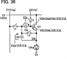
36 veranschaulicht den Betrieb einer Halbleitervorrichtung; 36 illustrates the operation of a semiconductor device;
37A bis 37D veranschaulichen jeweils die Struktur einer Halbleitervorrichtung; 37A to 37D each illustrate the structure of a semiconductor device;
38A bis 38D veranschaulichen jeweils die Struktur einer Halbleitervorrichtung; 38A to 38D each illustrate the structure of a semiconductor device;
39 veranschaulicht die Struktur einer Halbleitervorrichtung; 39 Fig. 10 illustrates the structure of a semiconductor device;
40 veranschaulicht die Struktur einer Halbleitervorrichtung; 40 Fig. 10 illustrates the structure of a semiconductor device;
41 veranschaulicht die Struktur einer Halbleitervorrichtung; 41 Fig. 10 illustrates the structure of a semiconductor device;
42A bis 42D veranschaulichen jeweils die Struktur einer Halbleitervorrichtung; 42A to 42D each illustrate the structure of a semiconductor device;
43A bis 43F veranschaulichen jeweils die Struktur einer Halbleitervorrichtung; 43A to 43F each illustrate the structure of a semiconductor device;
44A bis 44F veranschaulichen jeweils die Struktur einer Halbleitervorrichtung; 44A to 44F each illustrate the structure of a semiconductor device;
45A bis 45D veranschaulichen jeweils die Struktur einer Halbleitervorrichtung; 45A to 45D each illustrate the structure of a semiconductor device;
46A bis 46D veranschaulichen jeweils die Struktur einer Halbleitervorrichtung; 46A to 46D each illustrate the structure of a semiconductor device;
47A bis 47D veranschaulichen jeweils die Struktur einer Halbleitervorrichtung; 47A to 47D each illustrate the structure of a semiconductor device;
48A bis 48D veranschaulichen jeweils die Struktur einer Halbleitervorrichtung; 48A to 48D each illustrate the structure of a semiconductor device;
49A bis 49D veranschaulichen jeweils die Struktur einer Halbleitervorrichtung; 49A to 49D each illustrate the structure of a semiconductor device;
50A bis 50D veranschaulichen jeweils die Struktur einer Halbleitervorrichtung; 50A to 50D each illustrate the structure of a semiconductor device;
51A bis 51D veranschaulichen jeweils die Struktur einer Halbleitervorrichtung; 51A to 51D each illustrate the structure of a semiconductor device;
52A bis 52D veranschaulichen jeweils die Struktur einer Halbleitervorrichtung; 52A to 52D each illustrate the structure of a semiconductor device;
53A bis 53D veranschaulichen jeweils die Struktur einer Halbleitervorrichtung; 53A to 53D each illustrate the structure of a semiconductor device;
54A bis 54D veranschaulichen jeweils die Struktur einer Halbleitervorrichtung; 54A to 54D each illustrate the structure of a semiconductor device;
55A bis 55C veranschaulichen jeweils die Struktur einer Halbleitervorrichtung; 55A to 55C each illustrate the structure of a semiconductor device;
56A bis 56C veranschaulichen jeweils die Struktur einer Halbleitervorrichtung; 56A to 56C each illustrate the structure of a semiconductor device;
57A bis 57D veranschaulichen jeweils die Struktur einer Halbleitervorrichtung; 57A to 57D each illustrate the structure of a semiconductor device;
58A bis 58D veranschaulichen jeweils die Struktur einer Halbleitervorrichtung; 58A to 58D each illustrate the structure of a semiconductor device;
59A bis 59C veranschaulichen jeweils die Struktur einer Halbleitervorrichtung; 59A to 59C each illustrate the structure of a semiconductor device;
60A bis 60C veranschaulichen jeweils die Struktur einer Halbleitervorrichtung; 60A to 60C each illustrate the structure of a semiconductor device;
61A bis 61D veranschaulichen jeweils die Struktur einer Halbleitervorrichtung; 61A to 61D each illustrate the structure of a semiconductor device;
62A bis 62D veranschaulichen jeweils die Struktur einer Halbleitervorrichtung; 62A to 62D each illustrate the structure of a semiconductor device;
63A bis 63D veranschaulichen jeweils die Struktur einer Halbleitervorrichtung; 63A to 63D each illustrate the structure of a semiconductor device;
64A bis 64D veranschaulichen jeweils die Struktur einer Halbleitervorrichtung; 64A to 64D each illustrate the structure of a semiconductor device;
65A bis 65D veranschaulichen jeweils die Struktur einer Halbleitervorrichtung; 65A to 65D each illustrate the structure of a semiconductor device;
66A bis 66D veranschaulichen jeweils die Struktur einer Halbleitervorrichtung; 66A to 66D each illustrate the structure of a semiconductor device;
67A bis 67C veranschaulichen jeweils die Struktur einer Halbleitervorrichtung; 67A to 67C each illustrate the structure of a semiconductor device;
68A bis 68C veranschaulichen jeweils die Struktur einer Halbleitervorrichtung; 68A to 68C each illustrate the structure of a semiconductor device;
69A bis 69D veranschaulichen jeweils die Struktur einer Halbleitervorrichtung; 69A to 69D each illustrate the structure of a semiconductor device;
70A bis 70D veranschaulichen jeweils die Struktur einer Halbleitervorrichtung; 70A to 70D each illustrate the structure of a semiconductor device;
71A bis 71D veranschaulichen jeweils die Struktur einer Halbleitervorrichtung; 71A to 71D each illustrate the structure of a semiconductor device;
72A bis 72D veranschaulichen jeweils den Betrieb einer Halbleitervorrichtung; 72A to 72D each illustrate the operation of a semiconductor device;
73A bis 73D veranschaulichen jeweils die Struktur einer Halbleitervorrichtung; 73A to 73D each illustrate the structure of a semiconductor device;
74A bis 74F veranschaulichen jeweils die Struktur einer Halbleitervorrichtung; 74A to 74F each illustrate the structure of a semiconductor device;
75A bis 75E veranschaulichen jeweils die Struktur einer Halbleitervorrichtung; 75A to 75E each illustrate the structure of a semiconductor device;
76A bis 76G veranschaulichen jeweils die Struktur einer Halbleitervorrichtung; 76A to 76G each illustrate the structure of a semiconductor device;
77 veranschaulicht die Struktur einer Halbleitervorrichtung; 77 Fig. 10 illustrates the structure of a semiconductor device;
78 veranschaulicht die Struktur einer Halbleitervorrichtung; 78 Fig. 10 illustrates the structure of a semiconductor device;
79 veranschaulicht die Struktur einer Halbleitervorrichtung; 79 Fig. 10 illustrates the structure of a semiconductor device;
80A und 80B veranschaulichen die Struktur einer Halbleitervorrichtung; 80A and 80B illustrate the structure of a semiconductor device;
81A bis 81C veranschaulichen jeweils die Struktur einer Halbleitervorrichtung; 81A to 81C each illustrate the structure of a semiconductor device;
82A bis 82D veranschaulichen jeweils die Struktur einer Halbleitervorrichtung; 82A to 82D each illustrate the structure of a semiconductor device;
83A und 83B veranschaulichen die Struktur einer Halbleitervorrichtung; 83A and 83B illustrate the structure of a semiconductor device;
84A und 84B veranschaulichen jeweils die Struktur einer Halbleitervorrichtung; 84A and 84B each illustrate the structure of a semiconductor device;
85A bis 85F veranschaulichen jeweils eine elektronische Vorrichtung; 85A to 85F each illustrate an electronic device;
86 veranschaulicht die Struktur einer Halbleitervorrichtung; 86 Fig. 10 illustrates the structure of a semiconductor device;
87A bis 87D veranschaulichen jeweils die Struktur einer Halbleitervorrichtung; 87A to 87D each illustrate the structure of a semiconductor device;
88A veranschaulicht die Struktur einer Halbleitervorrichtung, und 88B ist ein Ablaufdiagramm; 88A illustrates the structure of a semiconductor device, and 88B is a flowchart;
89 stellt Berechnungsergebnisse dar; 89 represents calculation results;
90 stellt Berechnungsergebnisse dar; und 90 represents calculation results; and
91 veranschaulicht eine elektronische Vorrichtung. 91 illustrates an electronic device.
Das beste Verfahren zur Ausführung der ErfindungThe best method for carrying out the invention
Ausführungsformen der vorliegenden Erfindung werden im Folgenden unter Bezugnahme auf die beigefügten Zeichnungen ausführlich beschrieben. Es ist zu beachten, dass die vorliegende Erfindung nicht auf die folgende Beschreibung beschränkt ist, und Kennern der Technik ist leicht ersichtlich, dass eine Vielfalt von Änderungen und Modifizierungen vorgenommen werden kann, ohne vom Gedanken und Umfang der vorliegenden Erfindung abzuweichen. Daher sollte die vorliegende Erfindung nicht auf die Beschreibungen der Ausführungsformen im Folgenden beschränkt werden. Bei im Folgenden angeführten Strukturen sind dieselben Abschnitte oder Abschnitte, die ähnliche Funktionen aufweisen, in verschiedenen Zeichnungen durch dieselben Bezugszeichen gekennzeichnet, und deren Beschreibung wird nicht wiederholt.Embodiments of the present invention will be described below in detail with reference to the accompanying drawings. It should be understood that the present invention is not limited to the following description, and it will be readily apparent to those skilled in the art that a variety of changes and modifications may be made without departing from the spirit and scope of the present invention. Therefore, the present invention should not be limited to the descriptions of the embodiments below. In the structures listed below, the same portions or portions having similar functions are denoted by the same reference numerals in various drawings, and their description will not be repeated.
Es ist zu beachten, dass was bei einer Ausführungsform (oder einem Teil des Inhalts) beschrieben wird, auf einen anderen Inhalt (oder einen Teil davon) in der Ausführungsform und/oder einen Inhalt (oder einen Teil davon), der bei einer weiteren Ausführungsform oder sonstigen Ausführungsformen beschrieben wird, angewendet, damit kombiniert oder dadurch ersetzt werden kann.It should be noted that what is described in one embodiment (or part of the content) refers to another content (or part thereof) in the embodiment and / or content (or part thereof) used in another embodiment or other embodiments is applied to be combined or replaced thereby.
Es ist zu beachten, dass die Struktur, die in einem Schaubild (oder einem Teil davon) in einer Ausführungsform veranschaulicht wird, mit der Struktur eines weiteren Teils des Schaubildes, der Struktur, die in einem anderen Schaubild (oder einem Teil davon) in der Ausführungsform veranschaulicht wird, und/oder der Struktur, die in einem Schaubild (oder einem Teil davon) in einer weiteren Ausführungsform oder sonstigen Ausführungsformen veranschaulicht wird, kombiniert werden kann.It is to be noted that the structure illustrated in a diagram (or a part thereof) in one embodiment has the structure of another part of the diagram, the structure shown in another diagram (or a part thereof) in FIG Embodiment, and / or the structure that is illustrated in a diagram (or a part thereof) in a further embodiment or other embodiments can be combined.
Es ist zu beachten, dass die Größe, die Dicke und Bereiche in den Zeichnungen in einigen Fällen der Deutlichkeit halber vergrößert sind. Folglich ist ein Aspekt der Ausführungsform der vorliegenden Erfindung nicht auf solche Maßstäbe beschränkt. Alternativ veranschaulichen Zeichnungen schematisch ein ideales Beispiel. Folglich ist ein Aspekt der Ausführungsform der vorliegenden Erfindung nicht auf Formen beschränkt, die in den Zeichnungen veranschaulicht sind, und er kann zum Beispiel aufgrund einer Fertigungstechnik oder einer Abweichung in den Abmessungen Varianten in der Form beinhalten.It should be noted that the size, thickness, and areas in the drawings are increased in some cases for the sake of clarity. Thus, one aspect of the embodiment of the present invention is not limited to such scales. Alternatively, drawings schematically illustrate an ideal example. Thus, one aspect of the embodiment of the present invention is not limited to the shapes illustrated in the drawings, and may include, for example, variations in shape due to a manufacturing technique or dimensional variation.
Es ist zu beachten, dass eine ausdrückliche Beschreibung „X und Y sind verbunden” den Fall, in dem X und Y elektrisch verbunden sind, den Fall, in dem X und Y funktional verbunden sind, und den Fall bezeichnet, in dem X und Y direkt verbunden sind. Hier kennzeichnet X und Y jeweils ein Objekt (z. B. eine Vorrichtung, ein Element, eine Schaltung, eine Leitung, eine Elektrode, einen Anschluss, eine leitfähige Dünnschicht, eine Schicht, ein Anzeigeelement, ein Licht emittierendes Element oder eine Last). Dementsprechend ist auch eine andere Verbindungsbeziehung als diejenigen, die in Zeichnungen und Texten dargestellt werden, ohne Beschränkung auf eine vorgegebene Verbindungsbeziehung, beispielsweise die Verbindungsbeziehung, die in den Zeichnungen und den Texten dargestellt wird, enthalten.It should be noted that an express description "X and Y are connected" denotes the case where X and Y are electrically connected, the case where X and Y are functionally connected, and the case where X and Y are are directly connected. Here, X and Y respectively designate an object (eg, a device, an element, a circuit, a line, an electrode, a terminal, a conductive thin film, a layer, a display element, a light-emitting element, or a load). Accordingly, a connection relationship other than those illustrated in drawings and texts is also included without limitation to a predetermined connection relationship, for example, the connection relationship shown in the drawings and the texts.
Beispielsweise können in dem Fall, in dem X und Y elektrisch verbunden sind, ein oder mehrere Elemente, die eine elektrische Verbindung zwischen X und Y ermöglichen (z. B. ein Schalter, ein Transistor, ein Kondensator, ein Induktor, ein Widerstand, eine Diode, ein Anzeigeelement, ein Licht emittierendes Element oder eine Last), zwischen X und Y verbunden sein. Ein Schalter wird so gesteuert, dass er ein- oder ausgeschaltet ist. Das heißt, ein Schalter ist leitend oder nichtleitend (ist eingeschaltet oder ausgeschaltet), um zu bestimmen, ob Strom dort hindurch fließt. Alternativ hat der Schalter eine Funktion, einen Strompfad auszuwählen oder zu ändern.For example, in the case where X and Y are electrically connected, one or more elements enabling an electrical connection between X and Y (eg, a switch, a transistor, a capacitor, an inductor, a resistor, a Diode, a display element, a light-emitting element or a load), between X and Y be connected. A switch is controlled to be on or off. That is, a switch is conductive or non-conductive (turned on or off) to determine if current is flowing therethrough. Alternatively, the switch has a function to select or change a current path.
Beispielsweise können in dem Fall, in dem X und Y funktional verbunden sind, eine oder mehrere Schaltungen, die eine funktionale Verbindung zwischen X und Y ermöglichen (z. B. eine logische Schaltung wie etwa ein Wechselrichter, eine NAND-Schaltung oder eine NOR-Schaltung; eine Signalwandlerschaltung wie etwa eine DA-Wandlerschaltung, eine AD-Wandlerschaltung oder eine Gammakorrekturschaltung; eine Potentialniveau-Wandlerschaltung wie zum Beispiel eine Leistungsversorgungsschaltung (z. B. ein DC-DC-Wandler, ein DC-DC-Aufwärtswandler oder ein DC-DC-Abwärtswandler) oder eine Niveauverschieberschaltung zum Ändern des Potentialniveaus eines Signals; eine Spannungsquelle; eine Stromquelle; ein Schaltkreis; eine Verstärkerschaltung wie zum Beispiel eine Schaltung, die eine Signalamplitude, die Strommenge oder dergleichen erhöhen kann, ein Operationsverstärker, eine Differentialverstärkerschaltung, eine Source-Folgerschaltung oder eine Pufferschaltung; eine Signalgeneratorschaltung; eine Speicherschaltung; und/oder eine Steuerschaltung), zwischen X und Y verbunden sein. Wenn eine Signalausgabe von X an Y gesendet wird, kann man davon sprechen, dass X und Y funktional verbunden sind, selbst wenn eine weitere Schaltung zwischen X und Y bereitgestellt wird.For example, in the case where X and Y are functionally connected, one or more circuits enabling a functional connection between X and Y (e.g., a logic circuit such as an inverter, a NAND circuit, or a NOR circuit) may be provided. A signal converter circuit such as a DA converter circuit, an AD converter circuit or a gamma correction circuit; a potential level converter circuit such as a power supply circuit (e.g., a DC-DC converter, a DC-DC boost converter, or a DC power converter); A step-down circuit for changing the potential level of a signal; a voltage source; a current source; a circuit; an amplifier circuit such as a circuit capable of increasing a signal amplitude, current amount or the like, an operational amplifier, a differential amplifier circuit, a source Follower circuit or a buffer circuit; a signal generator circuit; a memory circuit; and / or a control circuit), be connected between X and Y. When a signal output from X is sent to Y. can be said to be that X and Y are functionally connected, even if another circuit between X and Y is provided.
Es ist zu beachten, dass eine ausdrückliche Beschreibung „X und Y sind verbunden” bedeutet, dass X und Y elektrisch verbunden sind, X und Y funktional verbunden sind, und X und Y direkt verbunden sind. Das heißt, die ausdrückliche Beschreibung „X und Y sind elektrisch verbunden” entspricht einem ausdrücklichen, einfachen Ausdruck „X und Y sind verbunden”.It should be noted that an explicit description "X and Y are connected" means that X and Y are electrically connected, X and Y are functionally connected, and X and Y are directly connected. That is, the express description "X and Y are electrically connected" corresponds to an explicit, simple phrase "X and Y are connected".
Selbst wenn unabhängige Komponenten in einem Schaltplan elektrisch miteinander verbunden sind, weist eine Komponente in manchen Fällen Funktionen einer Vielzahl von Komponenten auf. Wenn zum Beispiel ein Teil einer Leitung auch als Elektrode dient, dient eine leitfähige Dünnschicht als Leitung und als Elektrode. Folglich beinhaltet eine „elektrische Verbindung” in dieser Patentschrift in ihrer Kategorie einen solchen Fall, in dem eine leitfähige Dünnschicht Funktionen einer Vielzahl von Komponenten aufweist.Even if independent components are electrically connected together in a circuit diagram, in some cases, a component has functions of a plurality of components. For example, when a part of a lead also serves as an electrode, a conductive thin film serves as a lead and an electrode. Thus, an "electrical connection" in this specification includes in its category such a case in which a conductive thin film has functions of a plurality of components.
Es ist zu beachten, dass es Kennern der Technik möglich sein könnte, einen Aspekt der Erfindung selbst dann zu bilden, wenn Abschnitte, mit denen sämtliche Anschlüsse eines aktiven Elements (z. B. eines Transistors oder einer Diode), eines passiven Elements (z. B. eines Kondensators oder eines Widerstandes) oder dergleichen verbunden sind, nicht spezifiziert sind. Mit anderen Worten, selbst wenn solche Abschnitte nicht spezifiziert sind, kann ein Aspekt der vorliegenden Erfindung offenkundig sein, und es kann in einigen Fällen festgestellt werden, dass ein Aspekt der vorliegenden Erfindung in dieser Patentschrift offengelegt wird, und dergleichen. Insbesondere ist es in dem Fall, in dem der Anschluss mit mehreren Abschnitten verbunden ist, nicht erforderlich, die Abschnitte zu spezifizieren, mit denen der Anschluss verbunden ist. Es könnte daher möglich sein, einen Aspekt der Erfindung zu bilden, indem Abschnitte spezifiziert werden, mit denen nur einige der Anschlüsse eines aktiven Elements (z. B. eines Transistors oder einer Diode), eines passiven Elements (z. B. eines Kondensators oder eines Widerstandes) oder dergleichen verbunden sind.It should be noted that those skilled in the art could conceivably form an aspect of the invention even if portions to which all terminals of an active element (eg, a transistor or a diode), a passive element (e.g. B. a capacitor or a resistor) or the like are not specified. In other words, even if such portions are not specified, an aspect of the present invention may be obvious, and it may be found in some cases that an aspect of the present invention is disclosed in this patent, and the like. In particular, in the case where the terminal is connected to multiple sections, it is not necessary to specify the sections to which the terminal is connected. It may therefore be possible to form an aspect of the invention by specifying portions with which only some of the terminals of an active element (eg, a transistor or a diode), a passive element (eg, a capacitor or a diode) a resistor) or the like are connected.
Es ist zu beachten, dass es Kennern der Technik möglich sein könnte, die Erfindung zu spezifizieren, wenn zumindest spezifiziert ist, wo eine Schaltung zu verbinden ist („Verbindungspunkt”). Alternativ könnte es Kennern der Technik möglich sein, die Erfindung zu spezifizieren, wenn zumindest eine Funktion einer Schaltung spezifiziert ist. Mit anderen Worten, wenn eine Funktion einer Schaltung spezifiziert ist, kann ein Aspekt der vorliegenden Erfindung offenkundig sein, und es kann in einigen Fällen festgestellt werden, dass ein Aspekt der vorliegenden Erfindung in dieser Patentschrift offengelegt wird, und dergleichen. Wenn ein Verbindungspunkt einer Schaltung spezifiziert ist, wird die Schaltung daher als ein Aspekt der Erfindung selbst dann offengelegt, wenn keine Funktion spezifiziert ist, und ein Aspekt der Erfindung kann entworfen werden. Wenn eine Funktion einer Schaltung spezifiziert ist, wird alternativ die Schaltung daher als ein Aspekt der Erfindung selbst dann offengelegt, wenn kein Verbindungspunkt spezifiziert ist, und ein Aspekt der Erfindung kann entworfen werden.It should be noted that those skilled in the art might be able to specify the invention when at least specifying where a circuit is to be connected ("connection point"). Alternatively, those skilled in the art might be able to specify the invention if at least one function of a circuit is specified. In other words, when a function of a circuit is specified, an aspect of the present invention may be obvious, and it may be found in some cases that an aspect of the present invention is disclosed in this patent, and the like. Therefore, when a connection point of a circuit is specified, the circuit is disclosed as an aspect of the invention even if no function is specified, and an aspect of the invention can be designed. Alternatively, when a function of a circuit is specified, the circuit is disclosed as an aspect of the invention even if no connection point is specified, and an aspect of the invention can be designed.
Es ist zu beachten, dass verschiedene Personen einen Aspekt der Ausführungsform der vorliegenden Erfindung umsetzen können. Es können jedoch unterschiedliche Personen an der Umsetzung der Erfindung beteiligt sein. Bei einem Sende-/Empfangssystem ist zum Beispiel folgender Fall möglich: Unternehmen A fertigt und verkauft Sendevorrichtungen, und Unternehmen B fertigt und verkauft Empfangsvorrichtungen. Als weiteres Beispiel ist bei einer Licht emittierenden Vorrichtung, die einen TFT und ein Licht emittierendes Element beinhaltet, folgender Fall möglich: Unternehmen A fertigt und verkauft Halbleitervorrichtungen, die TFTs beinhalten, und Unternehmen B kauft die Halbleitervorrichtungen, stellt Licht emittierende Elemente für die Halbleitervorrichtungen bereit und stellt Licht emittierende Vorrichtungen fertig.It should be noted that various persons may implement an aspect of the embodiment of the present invention. However, different persons may be involved in the implementation of the invention. For example, in a transceiver system, the following case is possible: Company A manufactures and sells transceivers, and Company B manufactures and sells transceivers. As another example, in a light emitting device including a TFT and a light emitting element, the following case is possible: Company A manufactures and sells semiconductor devices including TFTs, and Company B buys the semiconductor devices, and provides light emitting elements for the semiconductor devices and complete light emitting devices.
In einem solchen Fall kann ein Aspekt der Erfindung so gebildet werden, dass eine Patentverletzung jeweils gegen Unternehmen A und Unternehmen B geltend gemacht werden kann. Das heißt, ein Aspekt der Erfindung, mit dem eine Patentverletzungsklage gegen Unternehmen A oder Unternehmen B eingereicht werden kann, ist offenkundig und kann als in dieser Patentschrift offengelegt betrachtet werden oder dergleichen. Beispielsweise kann bei einem Sende-/Empfangssystem ein Aspekt der Erfindung durch lediglich eine Sendevorrichtung gebildet werden, und ein Aspekt der Erfindung kann durch lediglich eine Empfangsvorrichtung gebildet werden. Diese Ausführungsformen der Erfindung sind offenkundig und können als in dieser Patentschrift offengelegt betrachtet werden oder dergleichen. Als weiteres Beispiel kann bei einer Licht emittierenden Vorrichtung, die einen TFT und ein Licht emittierendes Element beinhaltet, ein Aspekt der Erfindung durch lediglich eine Halbleitervorrichtung gebildet werden, die einen TFT beinhaltet, und ein Aspekt der Erfindung kann durch lediglich eine Licht emittierende Vorrichtung gebildet werden, die einen TFT und ein Licht emittierendes Element beinhaltet. Diese Ausführungsformen der Erfindung sind offenkundig und können als in dieser Patentschrift offengelegt betrachtet werden oder dergleichen.In such a case, an aspect of the invention may be formed so that a patent infringement can be asserted against Company A and Company B, respectively. That is, an aspect of the invention with which a patent infringement claim against Company A or Company B may be filed is obvious and may be considered to be disclosed in this patent or the like. For example, in a transmission / reception system, an aspect of the invention may be constituted by only one transmission device, and an aspect of the invention may be constituted by only one reception device. These embodiments of the invention are obvious and may be considered as disclosed in this patent or the like. As another example, in a light-emitting device including a TFT and a light-emitting element, an aspect of the invention may be formed by only a semiconductor device including a TFT, and an aspect of the invention may be formed by only a light-emitting device which includes a TFT and a light-emitting element. These embodiments of the invention are obvious and may be considered as disclosed in this patent or the like.
(Ausführungsform 1) (Embodiment 1)
Ein Aspekt der vorliegenden Erfindung kann nicht nur als Bildpunkt verwendet werden, der ein Licht emittierendes Element beinhaltet, sondern als eine Vielfalt von Schaltungen. Er kann zum Beispiel entweder als analoge Schaltung oder als Schaltung verwendet werden, die als Stromquelle dient. Zunächst werden bei dieser Ausführungsform Beispiele für ein Grundprinzip einer Schaltung beschrieben, die in der vorliegenden Erfindung offengelegt wird.An aspect of the present invention can be used not only as a pixel including a light-emitting element but as a variety of circuits. For example, it can be used either as an analog circuit or as a circuit serving as a power source. First, in this embodiment, examples of a basic principle of a circuit disclosed in the present invention will be described.
Eine Halbleitervorrichtung gemäß einem Aspekt der vorliegenden Erfindung beinhaltet zumindest zum Beispiel einen Transistor und ein Element, das eine Funktion hat, eine elektrische Ladung freizugeben, die zwischen einem Gate und einer Source des Transistors gespeichert ist, wohingegen das Potential des Gate fest ist. Mit diesem Element kann die Halbleitervorrichtung gemäß einem Aspekt der vorliegenden Erfindung Schwankungen im Drain-Strom aufgrund der Schwellenspannung, Beweglichkeit des Transistors oder dergleichen korrigieren.A semiconductor device according to an aspect of the present invention includes at least, for example, a transistor and an element having a function of releasing an electric charge stored between a gate and a source of the transistor, whereas the potential of the gate is fixed. With this element, the semiconductor device according to one aspect of the present invention can correct for variations in the drain current due to the threshold voltage, mobility of the transistor, or the like.
Bei einer Schaltung 100 in 1A handelt es sich um eine Halbleitervorrichtung gemäß einem Aspekt der vorliegenden Erfindung. Die Schaltung 100 beinhaltet einen Schalter 11, einen Schalter 12, einen Schalter 13, einen Transistor 101, einen Kondensator 102 und einen Kondensator 103. Es ist zu beachten, dass 1A den Fall darstellt, in dem es sich bei dem Transistor 101 um einen n-Kanal-Transistor handelt.At a circuit 100 in 1A it is a semiconductor device according to one aspect of the present invention. The circuit 100 includes a switch 11 , a switch 12 , a switch 13 , a transistor 101 , a capacitor 102 and a capacitor 103 , It should be noted that 1A represents the case in which it is the transistor 101 is an n-channel transistor.
Im Besonderen hat der Schalter 11 in 1A eine Funktion, das Leiten zwischen einer Leitung 21 und einer Elektrode (einem Anschluss) des Kondensators 102 oder 103 zu steuern. Der Schalter 12 hat eine Funktion, das Leiten zwischen einer Leitung 22 und der anderen Elektrode (dem Anschluss) des Kondensators 102 und zwischen der Leitung 22 und einem Gate des Transistors 101 zu steuern. Der Schalter 13 hat eine Funktion, das Leiten zwischen einer Source bzw. einem Drain des Transistors 101 oder der anderen Elektrode (dem Anschluss) des Kondensators 103 und der einen Elektrode des Kondensators 102 oder 103 zu steuern. Von der Source und dem Drain des Transistors 101 ist die/der andere mit einer Leitung 23 verbunden. Die Source bzw. der Drain des Transistors 101 oder die andere Elektrode (der Anschluss) des Kondensators 103 ist mit einer Leitung 24 verbunden.In particular, the switch has 11 in 1A a function that conducts between a line 21 and an electrode (a terminal) of the capacitor 102 or 103 to control. The desk 12 has a function that conducts between a line 22 and the other electrode (the terminal) of the capacitor 102 and between the line 22 and a gate of the transistor 101 to control. The desk 13 has a function of conducting between a source and a drain of the transistor 101 or the other electrode (terminal) of the capacitor 103 and the one electrode of the capacitor 102 or 103 to control. From the source and the drain of the transistor 101 is the other one with a lead 23 connected. The source or the drain of the transistor 101 or the other electrode (terminal) of the capacitor 103 is with a lead 24 connected.
Es ist zu beachten, dass die Begriffe „Source” (Source-Anschluss, Source-Bereich oder Source-Elektrode) und „Drain” (Drain-Anschluss, Drain-Bereich oder Drain-Elektrode) eines Transistors abhängig von der Polarität des Transistors oder den Niveaus von Potentialen, die an die Source und den Drain angelegt werden, miteinander vertauscht werden. Was eine Source und einen Drain in einem n-Kanaltransistor betrifft, so wird im Allgemeinen als Source bezeichnet, woran ein niedrigeres Potential angelegt wird, und es wird als Drain bezeichnet, woran ein höheres Potential angelegt wird. Was eine Source und einen Drain in einem p-Kanaltransistor betrifft, so wird ferner als Drain bezeichnet, woran ein niedrigeres Potential angelegt wird, und es wird als Source bezeichnet, woran ein höheres Potential angelegt wird. In dieser Patentschrift werden im Übrigen die Namen der Source und des Drain abhängig von dem Verhältnis der Potentiale miteinander vertauscht, wenngleich in einigen Fällen der Einfachheit halber ein Verbindungsverhältnis des Transistors beschrieben wird, das davon ausgeht, dass die Source und der Drain festgelegt sind. Folglich wird in einigen Fällen ein Abschnitt, der als Source dient, oder ein Abschnitt, der als Drain dient, nicht als Source oder Drain bezeichnet. In diesem Fall könnte beispielsweise entweder die Source oder der Drain als erster Anschluss, erste Elektrode oder erster Bereich bezeichnet werden, und der andere der Source und des Drain könnte als zweiter Anschluss, zweite Elektrode oder zweiter Bereich bezeichnet werden.It should be noted that the terms "source" (source terminal, source region or source electrode) and "drain" (drain terminal, drain region or drain electrode) of a transistor depend on the polarity of the transistor or the levels of potentials applied to the source and the drain are interchanged. As to a source and a drain in an n-channel transistor, it is generally referred to as a source to which a lower potential is applied, and it is called a drain, to which a higher potential is applied. As to a source and a drain in a p-channel transistor, it is also referred to as a drain, to which a lower potential is applied, and it is referred to as a source, to which a higher potential is applied. Incidentally, in this patent, the names of the source and the drain are interchanged depending on the ratio of the potentials, although in some cases, for convenience, a connection ratio of the transistor assuming that the source and the drain are fixed will be described. Thus, in some cases, a portion serving as a source or a portion serving as a drain will not be referred to as source or drain. In this case, for example, either the source or the drain could be referred to as the first terminal, the first electrode or the first area, and the other of the source and the drain could be referred to as a second terminal, second electrode or second area.
Es ist zu beachten, dass es sich bei einem Schalter um ein Element handelt, das eine Funktion hat, so zu funktionieren, dass es Leiten und Nichtleiten zwischen seinen Anschlüssen umschaltet, und eine Funktion hat zu bestimmen, ob Strom zwischen ihnen fließt. Alternativ hat der Schalter eine Funktion, einen Strompfad auszuwählen und zu ändern. Beispielsweise hat der Schalter eine Funktion zu bestimmen, ob ein Strom durch einen Pfad 1 oder einen Pfad 2 fließen kann, und die Pfade umzuschalten. Beispielsweise kann ein elektrischer Schalter oder ein mechanischer Schalter als Schalter verwendet werden. Im Besonderen kann der Schalter mithilfe eine Transistors, einer Diode oder eines Schalters ausgebildet sein, der durch eine Technologie mikroelektromechanischer Systeme (MEMS) ausgebildet ist, wie zum Beispiel eine digitale Mikrospiegelvorrichtung (digital micro mirror device, DMD). Alternativ kann es sich bei dem Schalter um eine logische Schaltung handeln, in der Transistoren kombiniert sind. Wenn ein Transistor als Schalter eingesetzt wird, besteht keine besondere Beschränkung für die Polarität (den Leitfähigkeitstyp) des Transistors. Es ist zu beachten, dass bevorzugt ein Transistor mit niedrigem Sperrstrom verwendet wird und die Polarität des Transistors bevorzugt entsprechend einem Eingangspotential ausgewählt wird.It should be noted that a switch is an element that has a function of functioning to switch conduction and non-conduction between its terminals, and has a function of determining whether current flows between them. Alternatively, the switch has a function of selecting and changing a rung. For example, the switch has a function of determining whether a current can flow through a path 1 or a path 2 and toggle the paths. For example, an electrical switch or a mechanical switch can be used as a switch. In particular, the switch may be formed by means of a transistor, a diode, or a switch formed by microelectromechanical system (MEMS) technology, such as a digital micro mirror device (DMD). Alternatively, the switch may be a logic circuit in which transistors are combined. When a transistor is used as a switch, there is no particular restriction on the polarity (conductivity type) of the transistor. It should be noted that it is preferable to use a transistor with a low reverse current and that the polarity of the transistor is preferably selected according to an input potential.
Beispiele für den Transistor mit niedrigem Sperrstrom sind ein Transistor, der mit einem LDD-Bereich ausgestattet ist, ein Transistor mit einer Multigate-Struktur und ein Transistor, dessen Kanalausbildungsbereich einen Oxidhalbleiter enthält. In dem Fall, in dem eine Kombination aus Transistoren als Schalter arbeitet, kann ein komplementärer Schalter eingesetzt werden, indem sowohl ein n-Kanal-Transistor als auch ein p-Kanal-Transistor eingesetzt werden. Ein komplementärer Schalter erzielt einen geeigneten Betrieb selbst dann, wenn ein Potential, das in den Schalter eingegeben wird, im Verhältnis zu einem Ausgangspotential verändert wird. Examples of the low reverse current transistor include a transistor provided with an LDD region, a transistor having a multi-gate structure, and a transistor whose channel formation region includes an oxide semiconductor. In the case where a combination of transistors operates as a switch, a complementary switch can be employed by employing both an n-channel transistor and a p-channel transistor. A complementary switch achieves proper operation even when a potential input to the switch is changed in proportion to an output potential.
Es ist zu beachten, dass, wenn ein Transistor als Schalter verwendet wird, der Schalter in einigen Fällen einen Eingangsanschluss (entweder eine Source oder einen Drain), einen Ausgangsanschluss (die/den anderen der Source und des Drain) und einen Anschluss zum Steuern eines Leitens (Gate) beinhaltet. Wenn demgegenüber eine Diode als Schalter verwendet wird, weist der Schalter in einigen Fällen keinen Anschluss zum Steuern eines Leitens auf. Wenn eine Diode als Schalter verwendet wird, kann daher die Anzahl der Leitungen zum Steuern von Anschlüssen im Vergleich zu dem Fall, in dem ein Transistor verwendet wird, verringert werden.It should be noted that when a transistor is used as a switch, in some cases the switch has an input terminal (either a source or a drain), an output terminal (the other of the source and the drain) and a terminal for controlling a Guiding (gate) includes. In contrast, when a diode is used as a switch, in some cases, the switch has no terminal for controlling conduction. Therefore, when a diode is used as a switch, the number of lines for controlling terminals can be reduced as compared with the case where a transistor is used.
Es ist zu beachten, dass zum Beispiel ein Transistor mit einer Struktur als Transistor verwendet werden kann, bei der Gates oberhalb und unterhalb eines Kanalausbildungsbereichs bereitgestellt werden. Durch Bereitstellen der Gates oberhalb und unterhalb einer Halbleiter-Dünnschicht wird eine Schaltungsstruktur bereitgestellt, bei der eine Vielzahl von Transistoren parallel verbunden ist. Auf diese Weise wird ein Kanalausbildungsbereich vergrößert, so dass die Menge des Stroms erhöht werden kann. Durch Einsetzen der Struktur, bei der die Gates oberhalb und unterhalb des Kanalausbildungsbereichs bereitgestellt werden, lässt sich leicht eine Verarmungsschicht ausbilden; auf diese Weise kann die Schwingung unter dem Schwellenwert (subthreshold swing, Wert S) verbessert werden.It should be noted that, for example, a transistor having a structure as a transistor in which gates are provided above and below a channel formation region may be used. By providing the gates above and below a semiconductor thin film, a circuit structure in which a plurality of transistors are connected in parallel is provided. In this way, a channel formation area is increased, so that the amount of the current can be increased. By employing the structure in which the gates are provided above and below the channel formation region, a depletion layer can be easily formed; in this way the oscillation below the threshold value (subthreshold swing, value S) can be improved.
Es ist zu beachten, dass zum Beispiel ein Transistor mit einer Struktur als Transistor verwendet werden kann, bei der eine Source-Elektrode oder eine Drain-Elektrode mit einem Kanalausbildungsbereich (oder einem Teil davon) überlappt. Durch Einsetzen der Struktur, bei der die Source-Elektrode oder die Drain-Elektrode mit dem Kanalausbildungsbereich (oder einem Teil davon) überlappt, kann ein instabiler Betrieb aufgrund elektrischer Ladung, die sich in einem Teil des Kanalausbildungsbereichs angesammelt hat, verhindert werden.It should be noted that, for example, a transistor having a structure as a transistor in which a source electrode or a drain electrode overlaps with a channel formation region (or a part thereof) may be used. By employing the structure in which the source electrode or the drain electrode overlaps with the channel formation region (or a part thereof), unstable operation due to electric charge accumulated in a part of the channel formation region can be prevented.
Es ist zu beachten, dass der Kondensator 102 oder 103 eine Struktur aufweisen kann, bei der zum Beispiel eine Isolierdünnschicht oder eine organische Dünnschicht zwischen Leitungen, Halbleiterschichten, Elektroden oder dergleichen angeordnet ist.It should be noted that the capacitor 102 or 103 may have a structure in which, for example, an insulating thin film or an organic thin film is disposed between lines, semiconductor layers, electrodes or the like.
Es ist zu beachten, dass die Schaltung 100 in 1A eine Last 104 beinhalten kann, wie in 1B veranschaulicht. In der Schaltung 100 in 1B ist die Last 104 zwischen der Source bzw. dem Drain des Transistors 101 oder der anderen Elektrode des Kondensators 103 und der Leitung 24 verbunden.It should be noted that the circuit 100 in 1A a burden 104 may include, as in 1B illustrated. In the circuit 100 in 1B is the burden 104 between the source and the drain of the transistor 101 or the other electrode of the capacitor 103 and the line 24 connected.
Es ist zu beachten, dass in dieser Patentschrift eine Last ein Objekt, das eine gleichrichtende Eigenschaft aufweist, ein Objekt, das eine Kapazität aufweist, ein Objekt, das einen Widerstand aufweist, eine Schaltung, die einen Schalter beinhaltet, eine Stromquellenschaltung oder dergleichen bedeutet. Beispielsweise weist eine Last, die eine gleichrichtende Eigenschaft aufweist, eine Strom-Spannung-Kennlinie auf, die abhängig von der Richtung einer angelegten Vorspannung unterschiedliche Widerstandswerte aufweist und eine elektrische Eigenschaft aufweist, die den meisten Strom nur in eine Richtung fließen lässt. Im Besonderen kann es sich bei der Last um ein Anzeigeelement (z. B. ein Flüssigkristallelement und ein EL-Element), ein Licht emittierendes Element (ein EL(Elektrolumineszenz)-Element, z. B. ein EL-Element, das organische und anorganische Materialien enthält, ein organisches EL-Element oder ein anorganisches EL-Element) und eine LED (z. B. eine weiße LED, eine rote LED, eine grüne LED oder eine blaue LED), einen Transistor (einen Transistor, der Licht entsprechend der Menge des Stroms emittiert), einen Elektronenemitter, einen Teil eines Anzeigeelements oder eines Licht emittierenden Elements (z. B. eine Bildpunktelektrode, eine Anode und eine Kathode) oder dergleichen handeln.It should be noted that in this specification, a load means an object having a rectifying property, an object having a capacitance, an object having a resistance, a circuit including a switch, a current source circuit, or the like. For example, a load having a rectifying property has a current-voltage characteristic that has different resistance values depending on the direction of an applied bias and has an electrical characteristic that allows most current to flow in one direction only. In particular, the load may be a display element (eg, a liquid crystal element and an EL element), a light-emitting element (an EL (electroluminescence) element, eg, an EL element, the organic and contains inorganic materials, an organic EL element or an inorganic EL element) and an LED (eg, a white LED, a red LED, a green LED, or a blue LED), a transistor (a transistor, the light corresponding the amount of current emitted), an electron emitter, a part of a display element or a light-emitting element (eg, a pixel electrode, an anode and a cathode), or the like.
1C veranschaulicht die Struktur einer Schaltung 100, die ein Licht emittierendes Element 104a als Last 104 verwendet. 1C veranschaulicht den Fall, in dem eine Anode des Licht emittierenden Elements 104a mit der Source bzw. dem Drain des Transistors 101 oder der anderen Elektrode des Kondensators 103 verbunden ist und eine Kathode des Licht emittierenden Elements 104a mit der Leitung 24 verbunden ist. 1C illustrates the structure of a circuit 100 that is a light-emitting element 104a as a burden 104 used. 1C illustrates the case where an anode of the light-emitting element 104a with the source and the drain of the transistor 101 or the other electrode of the capacitor 103 is connected and a cathode of the light-emitting element 104a with the line 24 connected is.
1D veranschaulicht die Struktur einer Schaltung 100, die ein Licht emittierendes Element 104b als Last 104 verwendet. 1D veranschaulicht den Fall, in dem eine Kathode des Licht emittierenden Elements 104b mit der Source bzw. dem Drain des Transistors 101 oder der anderen Elektrode des Kondensators 103 verbunden ist und eine Anode des Licht emittierenden Elements 104b mit der Leitung 24 verbunden ist. Es ist zu beachten, dass 1D den Fall darstellt, in dem es sich bei dem Transistor 101 um einen p-Kanal-Transistor handelt. 1D illustrates the structure of a circuit 100 that is a light-emitting element 104b as a burden 104 used. 1D illustrates the case where a cathode of the light-emitting element 104b with the source and the drain of the transistor 101 or the other electrode of the capacitor 103 is connected and an anode of the light-emitting element 104b with the line 24 connected is. It should be noted that 1D represents the case in which it is the transistor 101 is a p-channel transistor.
Eine Halbleitervorrichtung gemäß einem Aspekt der vorliegenden Erfindung kann zum Beispiel eine beliebige Schaltung, die der Schaltung 100 eine konstante Spannung oder ein Signal zuführt, wie auch beliebige der Schaltungen 100 beinhalten, die in 1A bis 1D veranschaulicht sind.A semiconductor device according to an aspect of the present invention may be, for example, any circuit corresponding to the circuit 100 supplying a constant voltage or signal, as well as any of the circuits 100 include that in 1A to 1D are illustrated.
In 2A bis 2D veranschaulichte Halbleitervorrichtungen beinhalten zusätzlich zu den Schaltungen 100 in 1A bis 1D eine Schaltung 201, die eine Funktion hat, der Leitung 21 eine konstante Spannung oder ein Signal zuzuführen, eine Schaltung 202, die eine Funktion hat, der Leitung 22 eine konstante Spannung oder ein Signal zuzuführen, eine Schaltung 203, die eine Funktion hat, der Leitung 23 eine konstante Spannung oder ein Signal zuzuführen, und eine Schaltung 204, die eine Funktion hat, der Leitung 24 eine konstante Spannung oder ein Signal zuzuführen.In 2A to 2D illustrated semiconductor devices include in addition to the circuits 100 in 1A to 1D a circuit 201 that has a function of lead 21 to supply a constant voltage or a signal, a circuit 202 that has a function of lead 22 to supply a constant voltage or a signal, a circuit 203 that has a function of lead 23 to supply a constant voltage or signal, and a circuit 204 that has a function of lead 24 to supply a constant voltage or a signal.
Im Besonderen hat die Schaltung 201 eine Funktion, der Leitung 21 ein Potential Vi1 oder ein Potential Vsig zuzuführen. Ein Beispiel für die Schaltung 201 ist ein Source-Treiber (eine Signalleitungs-Treiberschaltung). Dementsprechend hat die Leitung 21 eine Funktion, das Potential Vi1 und/oder das Potential Vsig zu senden oder zuzuführen. Die Leitung 21 dient als Videosignalleitung. Alternativ dient die Leitung 21 als Initialisierungsleitung.In particular, the circuit has 201 a function of the line 21 to supply a potential Vi1 or a potential Vsig. An example of the circuit 201 is a source driver (a signal line driver circuit). Accordingly, the line has 21 a function to send or supply the potential Vi1 and / or the potential Vsig. The administration 21 serves as a video signal line. Alternatively, the line is used 21 as initialization line.
Bei dem Potential Vi1 handelt es sich zum Beispiel um ein Potential zum Initialisieren des Potentials jedes Knotens in der Schaltung 100. Alternativ handelt es sich bei dem Potential Vi1 zum Beispiel um ein Potential zum Zuführen elektrischer Ladung zu dem Kondensator 102. Alternativ handelt es sich bei dem Potential Vi1 zum Beispiel um ein Potential zum Einschalten des Transistors 101. Es ist zu beachten, dass das Potential Vi1 bevorzugt konstant ist; ein Aspekt der Ausführungsform der vorliegenden Erfindung ist jedoch nicht darauf beschränkt. Das Potential Vi1 kann wie ein Impulssignal variieren.The potential Vi1 is, for example, a potential for initializing the potential of each node in the circuit 100 , Alternatively, the potential Vi1 is, for example, a potential for supplying electric charge to the capacitor 102 , Alternatively, the potential Vi1 is, for example, a potential for turning on the transistor 101 , It should be noted that the potential Vi1 is preferably constant; however, an aspect of the embodiment of the present invention is not limited thereto. The potential Vi1 may vary like a pulse signal.
Es ist als Beispiel zu beachten, dass das Potential Vi1 der Schaltung 100 zugeführt wird, bevor das Potential Vsig der Schaltung 100 zugeführt wird.It should be noted as an example that the potential Vi1 of the circuit 100 is fed before the potential Vsig of the circuit 100 is supplied.
Bei dem Potential Vsig handelt es sich um ein Potential zum Steuern der Menge des Drain-Stroms des Transistors 101. Bei der in 2B veranschaulichten Halbleitervorrichtung wird der Drain-Strom der Last 104 zugeführt. Bei der in 2C veranschaulichten Halbleitervorrichtung wird der Drain-Strom dem Licht emittierenden Element 104a zugeführt. Bei der in 2D veranschaulichten Halbleitervorrichtung wird der Drain-Strom dem Licht emittierenden Element 104b zugeführt. Wenn zum Beispiel der Drain-Strom des Transistors 101 auf einem konstanten Wert gehalten wird, ist das Niveau des Potentials Vsig konstant eingestellt. Wenn demgegenüber zum Beispiel der Drain-Strom des Transistors 101 nicht auf einen konstanten Wert eingestellt ist, wird das Niveau des Potentials Vsig im Laufe der Zeit verändert. Beispielsweise handelt es sich bei dem Potential Vsig um ein Videosignal und/oder ein Analogsignal. Ein Aspekt der Ausführungsform der vorliegenden Erfindung ist jedoch nicht hierauf beschränkt; das Potential Vsig kann auch ein konstantes Potential sein.The potential Vsig is a potential for controlling the amount of the drain current of the transistor 101 , At the in 2 B The semiconductor device illustrated becomes the drain current of the load 104 fed. At the in 2C In the illustrated semiconductor device, the drain current becomes the light-emitting element 104a fed. At the in 2D In the illustrated semiconductor device, the drain current becomes the light-emitting element 104b fed. If, for example, the drain current of the transistor 101 is kept at a constant value, the level of the potential Vsig is set constant. In contrast, when, for example, the drain current of the transistor 101 is not set to a constant value, the level of the potential Vsig is changed over time. For example, the potential Vsig is a video signal and / or an analog signal. However, an aspect of the embodiment of the present invention is not limited thereto; the potential Vsig can also be a constant potential.
Die Schaltung 202 hat eine Funktion, der Leitung 22 ein Potential Vi2 zuzuführen. Ein Beispiel für die Schaltung 202 ist eine Leistungsversorgungsschaltung. Dementsprechend hat die Leitung 22 eine Funktion, das Potential Vi2 zu senden oder zuzuführen. Alternativ dient die Leitung 22 als Initialisierungsleitung. Es ist zu beachten, dass das Potential der Leitung 22 bevorzugt konstant ist; ein Aspekt der Ausführungsform der vorliegenden Erfindung ist jedoch nicht darauf beschränkt. Das Potential der Leitung 22 kann wie ein Impulssignal variieren.The circuit 202 has a function, the line 22 to supply a potential Vi2. An example of the circuit 202 is a power supply circuit. Accordingly, the line has 22 a function to send or supply the potential Vi2. Alternatively, the line is used 22 as initialization line. It should be noted that the potential of the line 22 is preferably constant; however, an aspect of the embodiment of the present invention is not limited thereto. The potential of the line 22 can vary like a pulse signal.
Bei dem Potential Vi2 handelt es sich um ein Potential zum Initialisieren des Potentials jedes Knotens (insbesondere des Gate des Transistors 101) in der Schaltung 100. In dem Fall in 2C ist das Potential Vi2 bevorzugt niedriger als oder gleich wie das Potential der Leitung 24. Auf diese Weise kann ein Strom verringert werden, der zu dem Licht emittierenden Element 104a fließt. In dem Fall in 2D ist das Potential Vi2 bevorzugt höher als oder gleich wie das Potential der Leitung 24. Auf diese Weise kann ein Strom verringert werden, der zu dem Licht emittierenden Element 104b fließt. Das Potential des Potentials Vi2 ist jedoch nicht hierauf beschränkt. Es ist zu beachten, dass das Potential Vi2 bevorzugt konstant ist; ein Aspekt der Ausführungsform der vorliegenden Erfindung ist jedoch nicht darauf beschränkt. Das Potential Vi2 kann wie ein Impulssignal variieren.The potential Vi2 is a potential for initializing the potential of each node (in particular, the gate of the transistor 101 ) in the circuit 100 , In the case in 2C the potential Vi2 is preferably lower than or equal to the potential of the line 24 , In this way, a current can be reduced, which leads to the light-emitting element 104a flows. In the case in 2D the potential Vi2 is preferably higher than or equal to the potential of the line 24 , In this way, a current can be reduced, which leads to the light-emitting element 104b flows. However, the potential of the potential Vi2 is not limited to this. It should be noted that the potential Vi2 is preferably constant; however, an aspect of the embodiment of the present invention is not limited thereto. The potential Vi2 may vary like a pulse signal.
Es ist zu beachten, dass die Leitung 22 mit einer weiteren Leitung oder einer Leitung verbunden sein kann, die in einer weiteren Schaltung 100 enthalten ist. Auf diese Weise kann die Anzahl von Leitungen verringert werden. It should be noted that the line 22 may be connected to another line or a line in another circuit 100 is included. In this way, the number of lines can be reduced.
Die Schaltung 203 hat eine Funktion, der Leitung 23 eine Versorgungsspannung (ein hohes Versorgungspotential oder ein niedriges Versorgungspotential), z. B. ein Potential VDD oder ein Potential VSS zuzuführen. Alternativ hat die Schaltung 203 eine Funktion, der Leitung 23 ein Signal zuzuführen. Beispiele für die Schaltung 203 sind eine Leistungsversorgungsschaltung, eine Impulsausgangsschaltung und eine Gate-Treiberschaltung. Dementsprechend hat die Leitung 23 eine Funktion, ein Leistungsversorgungspotential oder ein Signal zu senden oder zuzuführen. Alternativ hat die Leitung 23 eine Funktion, dem Transistor 101 einen Strom zuzuführen. Alternativ hat die Leitung 23 eine Funktion, der Last 104 einen Strom zuzuführen. Die Leitung 23 dient als Leistungsversorgungsleitung. Alternativ dient die Leitung 23 als Stromversorgungsleitung. Es ist zu beachten, dass das Potential der Leitung 23 bevorzugt konstant ist; ein Aspekt der Ausführungsform der vorliegenden Erfindung ist jedoch nicht darauf beschränkt. Das Potential der Leitung 23 kann wie ein Impulssignal variieren. Beispielsweise kann es sich bei dem Potential der Leitung 23 um ein Potential handeln, bei dem nicht nur eine Vorspannung in Durchlassrichtung, sondern auch eine Vorspannung in Sperrrichtung an die Last 104 angelegt wird.The circuit 203 has a function, the line 23 a supply voltage (a high supply potential or a low supply potential), z. B. supply a potential VDD or a potential VSS. Alternatively, the circuit has 203 a function of the line 23 to supply a signal. Examples of the circuit 203 are a power supply circuit, a pulse output circuit and a gate driver circuit. Accordingly, the line has 23 to send or deliver a function, a power supply potential or a signal. Alternatively, the line has 23 a function, the transistor 101 to supply a current. Alternatively, the line has 23 a function, the load 104 to supply a current. The administration 23 serves as power supply line. Alternatively, the line is used 23 as power supply line. It should be noted that the potential of the line 23 is preferably constant; however, an aspect of the embodiment of the present invention is not limited thereto. The potential of the line 23 can vary like a pulse signal. For example, it may be at the potential of the line 23 to act a potential in which not only a bias in the forward direction, but also a bias in the reverse direction to the load 104 is created.
Die Schaltung 204 hat eine Funktion, der Leitung 24 beispielsweise eine Versorgungsspannung (ein niedriges Versorgungspotential oder ein hohes Versorgungspotential), z. B. ein Potential Vcat zuzuführen. Ein Beispiel für die Schaltung 204 ist eine Leistungsversorgungsschaltung. Dementsprechend hat die Leitung 24 eine Funktion, ein Leistungsversorgungspotential zu senden oder zuzuführen. Alternativ hat die Leitung 24 eine Funktion, der Last 104 einen Strom zuzuführen. Alternativ hat die Leitung 24 eine Funktion, dem Transistor 101 einen Strom zuzuführen. Die Leitung 24 dient als gemeinsame Leitung. Alternativ dient die Leitung 24 als negative Leitung. Alternativ dient die Leitung 24 als positive Leitung. Es ist zu beachten, dass das Potential der Leitung 24 bevorzugt konstant ist; ein Aspekt der Ausführungsform der vorliegenden Erfindung ist jedoch nicht darauf beschränkt. Das Potential der Leitung 24 kann wie ein Impulssignal variieren. Beispielsweise kann es sich bei dem Potential der Leitung 24 um ein Potential handeln, bei dem nicht nur eine Vorspannung in Durchlassrichtung, sondern auch eine Vorspannung in Sperrrichtung an die Last 104 angelegt wird.The circuit 204 has a function, the line 24 For example, a supply voltage (a low supply potential or a high supply potential), z. B. supply a potential Vcat. An example of the circuit 204 is a power supply circuit. Accordingly, the line has 24 a function to send or supply a power supply potential. Alternatively, the line has 24 a function, the load 104 to supply a current. Alternatively, the line has 24 a function, the transistor 101 to supply a current. The administration 24 serves as a common line. Alternatively, the line is used 24 as a negative line. Alternatively, the line is used 24 as a positive lead. It should be noted that the potential of the line 24 is preferably constant; however, an aspect of the embodiment of the present invention is not limited thereto. The potential of the line 24 can vary like a pulse signal. For example, it may be at the potential of the line 24 to act a potential in which not only a bias in the forward direction, but also a bias in the reverse direction to the load 104 is created.
Eine Differenz zwischen dem Potential VDD und dem Potential Vcat legt die Richtung des Drain-Stroms des Transistors 101 fest. Wenn zum Beispiel das Potential VDD höher als das Potential Vcat ist, fließt ein Strom von der Leitung 23 zu der Leitung 24. Wenn das Potential der Leitung 23 gleich hoch wie das Potential VSS und niedriger als das Potential Vcat ist, fließt ein Strom von der Leitung 24 zu der Leitung 23.A difference between the potential VDD and the potential Vcat sets the direction of the drain current of the transistor 101 firmly. For example, when the potential VDD is higher than the potential Vcat, a current flows from the line 23 to the line 24 , If the potential of the line 23 is equal to the potential VSS and lower than the potential Vcat, a current flows from the line 24 to the line 23 ,
Es ist zu beachten, dass die Halbleitervorrichtungen in den 2A bis 2D zusätzlich zu der Schaltung 100 jeweils zum Beispiel die Schaltungen 201, 202, 203 und 204 beinhalten. Eine Halbleitervorrichtung gemäß einem Aspekt der vorliegenden Erfindung beinhaltet jedoch nicht zwingend sämtliche der Schaltungen 201, 202, 203 und 204 und kann nur eine oder einige dieser Schaltungen beinhalten.It should be noted that the semiconductor devices in the 2A to 2D in addition to the circuit 100 in each case, for example, the circuits 201 . 202 . 203 and 204 include. However, a semiconductor device according to an aspect of the present invention does not necessarily include all of the circuits 201 . 202 . 203 and 204 and may include only one or some of these circuits.
Der Transistor 101 dient zum Beispiel zumindest als Stromquelle. Dementsprechend hat der Transistor 101 zum Beispiel eine Funktion, einen im Wesentlichen konstanten Strom selbst dann zuzuführen, wenn der Pegel einer Spannung, die über beide Enden (zwischen der Source und dem Drain) des Transistors 101 angelegt ist, verändert wird. Alternativ hat der Transistor 101 zum Beispiel eine Funktion, der Last 104 einen im Wesentlichen konstanten Strom selbst dann zuzuführen, wenn das Potential der Last 104 verändert wird. Alternativ hat der Transistor 101 zum Beispiel eine Funktion, einen im Wesentlichen konstanten Strom selbst dann zuzuführen, wenn das Potential der Leitung 23 verändert wird.The transistor 101 For example, at least serves as a power source. Accordingly, the transistor has 101 for example, a function of supplying a substantially constant current even when the level of a voltage across both ends (between the source and the drain) of the transistor 101 is created, is changed. Alternatively, the transistor has 101 for example, a function, the load 104 supplying a substantially constant current even when the potential of the load 104 is changed. Alternatively, the transistor has 101 for example, a function of supplying a substantially constant current even when the potential of the line 23 is changed.
Es ist zu beachten, dass ein Aspekt der Ausführungsform der vorliegenden Erfindung nicht hierauf beschränkt ist; der Transistor 101 dient nicht zwingend als Stromquelle. Der Transistor 101 kann zum Beispiel als Schalter dienen.It should be noted that one aspect of the embodiment of the present invention is not limited thereto; the transistor 101 does not necessarily serve as a power source. The transistor 101 can serve as a switch, for example.
Es ist zu beachten, dass eine Spannungsquelle als Leistungsquelle vorhanden ist, die sich von einer Stromquelle unterscheidet. Die Spannungsquelle hat eine Funktion, eine konstante Spannung selbst dann zuzuführen, wenn ein Strom verändert wird, der durch eine Schaltung fließt, die mit der Spannungsquelle verbunden ist. Dementsprechend haben die Spannungsquelle und die Stromquelle eine Funktion, Spannung bzw. Strom zuzuführen. Die Funktion der Spannungsquelle und die Funktion der Stromquelle unterscheiden sich jedoch in dem, was bei einem konstanten Pegel zugeführt wird, selbst wenn ein Faktor verändert wird. Die Stromquelle hat eine Funktion, einen konstanten Strom selbst dann zuzuführen, wenn eine Spannung über beide Enden verändert wird. Die Spannungsquelle hat eine Funktion, eine konstante Spannung selbst dann zuzuführen, wenn ein Strom verändert wird.It should be noted that there is a power source as a power source that is different from a power source. The voltage source has a function of supplying a constant voltage even when a current flowing through a circuit connected to the power source is changed. Accordingly, the power source and the power source have a function of supplying power. However, the function of the voltage source and the function of the current source differ in what is supplied at a constant level even if a factor is changed. The power source has a function of supplying a constant current even when a voltage exceeds both ends are changed. The voltage source has a function of supplying a constant voltage even when a current is changed.
Es ist zu beachten, dass die 1A bis 1D und dergleichen jeweils ein Beispiel für eine Schaltungsstruktur veranschaulichen; auf diese Weise kann ein Transistor zusätzlich bereitgestellt werden. Demgegenüber ist es bei jedem Knoten in den 1A bis 1D und dergleichen möglich, keinen zusätzlichen Transistor, Schalter, kein zusätzliches passives Element oder dergleichen bereitzustellen. Beispielsweise ist es möglich, keinen zusätzlichen Transistor bereitzustellen, der direkt mit einem Knoten, an dem Anschlüsse von Schaltern miteinander verbunden sind, einem Knoten, an dem Anschlüsse eines Transistors miteinander verbunden sind, und/oder einem Knoten verbunden ist, an dem Anschlüsse einer Last miteinander verbunden sind. Dementsprechend ist es zum Beispiel möglich, nur den Transistor 101 direkt mit einem Knoten zu verbinden, an dem die Last 104, der Transistor 101, der Kondensator 103 und der Schalter 13 miteinander verbunden sind, und es ist möglich, keinen weiteren Transistor direkt mit dem Knoten zu verbinden.It should be noted that the 1A to 1D and the like, respectively, illustrate an example of a circuit structure; In this way, a transistor can be additionally provided. In contrast, it is at each node in the 1A to 1D and the like, it is possible to provide no additional transistor, switch, additional passive element or the like. For example, it is possible to provide no additional transistor directly connected to a node at which terminals of switches are connected to each other, a node to which terminals of a transistor are connected to each other, and / or a node to terminals of a load connected to each other. Accordingly, it is possible, for example, only the transistor 101 connect directly to a node where the load is 104 , the transistor 101 , the capacitor 103 and the switch 13 are interconnected, and it is possible not to connect another transistor directly to the node.
Auf diese Weise kann eine Schaltung mit einer geringen Anzahl von Transistoren in dem Fall ausgebildet werden, in dem kein zusätzlicher Transistor bereitgestellt wird.In this way, a circuit having a small number of transistors can be formed in the case where no additional transistor is provided.
Es ist zu beachten, dass es sich bei dem Schalter 11, dem Schalter 12 und dem Schalter 13 in den Schaltungen 100 in 1A bis 1D und 2A bis 2D um Transistoren handeln kann.It should be noted that this is the switch 11 , the switch 12 and the switch 13 in the circuits 100 in 1A to 1D and 2A to 2D can be about transistors.
3A bis 3D veranschaulichen die Strukturen von Schaltungen 100, die den Schaltungen 100 in 1A bis 1D entsprechen, die jeweils einen Transistor 11t als Schalter 11, einen Transistor 12t als Schalter 12 und einen Transistor 13t als Schalter 13 verwenden. 3A bis 3C veranschaulichen den Fall, in dem es sich bei dem Transistor 11t, dem Transistor 12t und dem Transistor 13t sämtlich um n-Kanal-Transistoren handelt. 3D veranschaulicht den Fall, in dem es sich bei dem Transistor 11t, dem Transistor 12t und dem Transistor 13t sämtlich um p-Kanal-Transistoren handelt. Wenn der Transistor 11t, der Transistor 12t und der Transistor 13t dieselbe Polarität aufweisen, können diese Transistoren in weniger Schritten gefertigt werden. Ein Aspekt der Ausführungsform der vorliegenden Erfindung ist jedoch nicht hierauf beschränkt; diese Transistoren können verschiedene Polaritäten aufweisen. 3A to 3D illustrate the structures of circuits 100 that the circuits 100 in 1A to 1D correspond, each one transistor 11t as a switch 11 , a transistor 12t as a switch 12 and a transistor 13t as a switch 13 use. 3A to 3C illustrate the case where the transistor 11t , the transistor 12t and the transistor 13t all are n-channel transistors. 3D illustrates the case where the transistor 11t , the transistor 12t and the transistor 13t all are p-channel transistors. When the transistor 11t , the transistor 12t and the transistor 13t have the same polarity, these transistors can be made in fewer steps. However, an aspect of the embodiment of the present invention is not limited thereto; these transistors can have different polarities.
Es ist zu beachten, dass in 3A bis 3D ein Gate des Transistors 11t mit einer Leitung 31 verbunden ist. Der Transistor 11t wird in Reaktion auf das Potential, das der Leitung 31 zugeführt wird, ein- oder ausgeschaltet. Ein Gate des Transistors 12t ist mit einer Leitung 32 verbunden. Der Transistor 12t wird in Reaktion auf das Potential, das der Leitung 32 zugeführt wird, ein- oder ausgeschaltet. Ein Gate des Transistors 13t ist mit einer Leitung 33 verbunden. Der Transistor 13t wird in Reaktion auf das Potential, das der Leitung 33 zugeführt wird, ein- oder ausgeschaltet. Daher sollte es sich bei den Potentialen der Leitungen 31 bis 33 bevorzugt um gepulste Potentiale und nicht um konstante handeln; ein Aspekt der Ausführungsform der vorliegenden Erfindung ist jedoch nicht hierauf beschränkt. Alternativ dienen die Leitungen 31 bis 33 jeweils als Gate-Signalleitung (eine Gate-Leitung), als Auswahlsignalleitung oder als Abtastleitung.It should be noted that in 3A to 3D a gate of the transistor 11t with a line 31 connected is. The transistor 11t is in response to the potential of that line 31 is supplied, on or off. A gate of the transistor 12t is with a lead 32 connected. The transistor 12t is in response to the potential of that line 32 is supplied, on or off. A gate of the transistor 13t is with a lead 33 connected. The transistor 13t is in response to the potential of that line 33 is supplied, on or off. Therefore, it should be at the potentials of the wires 31 to 33 preferably pulsed potentials and not constant; however, an aspect of the embodiment of the present invention is not limited thereto. Alternatively, the lines serve 31 to 33 each as a gate signal line (a gate line), as a selection signal line or as a scanning line.
Es ist zu beachten, dass zumindest zwei dieser Leitungen 31 bis 33 miteinander verbunden sein können. Alternativ kann zumindest eine dieser Leitungen 31 bis 33 mit zumindest einer der Leitungen 31 bis 33 in einer weiteren Schaltung 100 verbunden sein.It should be noted that at least two of these lines 31 to 33 can be connected to each other. Alternatively, at least one of these lines 31 to 33 with at least one of the lines 31 to 33 in another circuit 100 be connected.
Eine Halbleitervorrichtung gemäß einem Aspekt der vorliegenden Erfindung kann zum Beispiel eine beliebige Schaltung, die der Schaltung 100 eine konstante Spannung oder ein Signal zuführt, wie auch beliebige der Schaltungen 100 beinhalten, die in 3A bis 3D veranschaulicht sind.A semiconductor device according to an aspect of the present invention may be, for example, any circuit corresponding to the circuit 100 supplying a constant voltage or signal, as well as any of the circuits 100 include that in 3A to 3D are illustrated.
In 4A bis 4D veranschaulichte Halbleitervorrichtungen beinhalten zusätzlich zu den Schaltungen 100 in 3A bis 3D eine Schaltung 205, die eine Funktion hat, der Leitung 31 eine konstante Spannung oder ein Signal zuzuführen, eine Schaltung 206, die eine Funktion hat, der Leitung 32 eine konstante Spannung oder ein Signal zuzuführen, und eine Schaltung 207, die eine Funktion hat, der Leitung 33 eine konstante Spannung oder ein Signal zuzuführen. Zu Beispielen für die Schaltungen 205, 206 und 207 zählen Gate-Treiber (Abtastleitungs-Treiberschaltungen).In 4A to 4D illustrated semiconductor devices include in addition to the circuits 100 in 3A to 3D a circuit 205 that has a function of lead 31 to supply a constant voltage or a signal, a circuit 206 that has a function of lead 32 to supply a constant voltage or signal, and a circuit 207 that has a function of lead 33 to supply a constant voltage or a signal. Examples of the circuits 205 . 206 and 207 include gate drivers (scan line driver circuits).
Es ist zu beachten, dass es sich bei den Schaltungen 201, 202, 203, 204, 205, 206 und 207 um dieselbe Schaltung oder um verschiedene Schaltungen handeln kann.It should be noted that the circuits 201 . 202 . 203 . 204 . 205 . 206 and 207 can be the same circuit or different circuits.
Es ist zu beachten, dass die Halbleitervorrichtungen in den 4A bis 4D zusätzlich zu der Schaltung 100 jeweils zum Beispiel die Schaltungen 205, 206 und 207 beinhalten. Eine Halbleitervorrichtung gemäß einem Aspekt der vorliegenden Erfindung beinhaltet jedoch nicht zwingend sämtliche der Schaltungen 205, 206 und 207 und kann nur eine oder einige dieser Schaltungen beinhalten.It should be noted that the semiconductor devices in the 4A to 4D in addition to the circuit 100 in each case, for example, the circuits 205 . 206 and 207 include. A semiconductor device according to However, one aspect of the present invention does not necessarily include all of the circuits 205 . 206 and 207 and may include only one or some of these circuits.
37A veranschaulicht die Struktur einer Schaltung 100, die der Schaltung 100 in 3C entspricht, in der es sich bei den Transistoren 101, 11t und 13t um n-Kanal-Transistoren handelt und es sich bei dem Transistor 12t um einen p-Kanal-Transistor handelt. 37B veranschaulicht die Struktur einer Schaltung 100, die der Schaltung 100 in 3D entspricht, in der es sich bei den Transistoren 101, 11t und 13t um p-Kanal-Transistoren handelt und es sich bei dem Transistor 12t um einen n-Kanal-Transistor handelt. Wie oben beschrieben, können Transistoren mit einer Vielfalt von Polaritäten verwendet werden. 37A illustrates the structure of a circuit 100 that of the circuit 100 in 3C corresponds, which is in the case of the transistors 101 . 11t and 13t are n-channel transistors and it is in the transistor 12t is a p-channel transistor. 37B illustrates the structure of a circuit 100 that of the circuit 100 in 3D corresponds, which is in the case of the transistors 101 . 11t and 13t are p-channel transistors and it is in the transistor 12t is an n-channel transistor. As described above, transistors having a variety of polarities can be used.
Eine Halbleitervorrichtung gemäß einem Aspekt der vorliegenden Erfindung kann zum Beispiel eine beliebige Schaltung, die der Schaltung 100 eine konstante Spannung oder ein Signal zuführt, wie auch beliebige der Schaltungen 100 beinhalten, die in 37A und 37B veranschaulicht sind.A semiconductor device according to an aspect of the present invention may be, for example, any circuit corresponding to the circuit 100 supplying a constant voltage or signal, as well as any of the circuits 100 include that in 37A and 37B are illustrated.
In 37C und 37D veranschaulichte Halbleitervorrichtungen beinhalten zusätzlich zu den Schaltungen 100 in 37A und 37B eine Schaltung 205, die eine Funktion hat, der Leitung 31 eine konstante Spannung oder ein Signal zuzuführen, eine Schaltung 206, die eine Funktion hat, der Leitung 32 eine konstante Spannung oder ein Signal zuzuführen, und eine Schaltung 207, die eine Funktion hat, der Leitung 33 eine konstante Spannung oder ein Signal zuzuführen.In 37C and 37D illustrated semiconductor devices include in addition to the circuits 100 in 37A and 37B a circuit 205 that has a function of lead 31 to supply a constant voltage or a signal, a circuit 206 that has a function of lead 32 to supply a constant voltage or signal, and a circuit 207 that has a function of lead 33 to supply a constant voltage or a signal.
Es ist zu beachten, dass die Halbleitervorrichtungen in den 37C und 37D als Beispiel zusätzlich zu der Schaltung 100 jeweils die Schaltungen 205, 206 und 207 beinhalten. Eine Halbleitervorrichtung gemäß einem Aspekt der vorliegenden Erfindung beinhaltet jedoch nicht zwingend sämtliche der Schaltungen 205, 206 und 207 und kann nur eine oder einige dieser Schaltungen beinhalten.It should be noted that the semiconductor devices in the 37C and 37D as an example in addition to the circuit 100 each of the circuits 205 . 206 and 207 include. However, a semiconductor device according to an aspect of the present invention does not necessarily include all of the circuits 205 . 206 and 207 and may include only one or some of these circuits.
In vielen Fällen arbeitet der Transistor 101 in einem Sättigungsbereich, wenn ein Strom dort hindurchfließt. Daher weist der Transistor 101 in den 3A bis 3D, 4A bis 4D und 37A bis 37D bevorzugt eine größere Kanallänge oder Gate-Länge als der Transistor 11t, der Transistor 12t und/oder der Transistor 13t auf. Wenn die Kanallänge oder die Gate-Länge erhöht wird, weisen Kennlinien in einem Sättigungsbereich eine flache Steigung auf; dementsprechend kann ein Knickeffekt verringert werden. Die Kanallänge oder Gate-Länge des Transistors 101 beträgt bevorzugt 5-mal oder mehr, ferner bevorzugt 10-mal oder mehr als die des Transistors 11t, des Transistors 12t und/oder des Transistors 13t. Als Beispiel beträgt die Kanallänge oder Gate-Länge des Transistors 101 bevorzugt 10 μm oder mehr, bevorzugter 20 μm oder mehr. Alternativ ist die Kanalbreite oder Gate-Breite des Transistors 101 größer als die des Transistors 11t, des Transistors 12t und/oder des Transistors 13t, so dass selbst in einem Sättigungsbereich ein großer Strom durch den Transistor 101 fließt. Die Kanalbreite oder Gate-Breite des Transistors 101 beträgt bevorzugt 5-mal oder mehr, ferner bevorzugt 10-mal oder mehr als die des Transistors 11t, des Transistors 12t und/oder des Transistors 13t. Die Kanalbreite oder Gate-Breite des Transistors 101 beträgt bevorzugt 20 μm oder mehr, bevorzugter 30 μm oder mehr. Es ist zu beachten, dass ein Aspekt einer Ausführungsform der vorliegenden Erfindung nicht darauf beschränkt ist.In many cases, the transistor works 101 in a saturation region when a current flows through it. Therefore, the transistor 101 in the 3A to 3D . 4A to 4D and 37A to 37D preferably a larger channel length or gate length than the transistor 11t , the transistor 12t and / or the transistor 13t on. When the channel length or the gate length is increased, characteristics in a saturation region have a flat slope; Accordingly, a kink effect can be reduced. The channel length or gate length of the transistor 101 is preferably 5 times or more, more preferably 10 times or more than that of the transistor 11t , the transistor 12t and / or the transistor 13t , As an example, the channel length or gate length of the transistor is 101 preferably 10 μm or more, more preferably 20 μm or more. Alternatively, the channel width or gate width of the transistor 101 larger than that of the transistor 11t , the transistor 12t and / or the transistor 13t so that even in a saturation region a large current passes through the transistor 101 flows. The channel width or gate width of the transistor 101 is preferably 5 times or more, more preferably 10 times or more than that of the transistor 11t , the transistor 12t and / or the transistor 13t , The channel width or gate width of the transistor 101 is preferably 20 μm or more, more preferably 30 μm or more. It should be noted that an aspect of an embodiment of the present invention is not limited thereto.
Im Folgenden wird der Betrieb einer Halbleitervorrichtung gemäß einem Aspekt der vorliegenden Erfindung beschrieben, wobei die in 1C veranschaulichte Schaltung 100 als Beispiel herangezogen wird.The following describes the operation of a semiconductor device according to an aspect of the present invention, wherein the in 1C illustrated circuit 100 is used as an example.
Der Betrieb der in 1C veranschaulichten Schaltung 100 kann hauptsächlich in einen ersten Betrieb, einen zweiten Betrieb, einen dritten Betrieb, einen vierten Betrieb und einen fünften Betrieb aufgeteilt werden. Es ist zu beachten, dass ein Aspekt einer Ausführungsform der vorliegenden Erfindung nicht darauf beschränkt ist und dass ein weiterer Betrieb hinzugefügt werden kann oder ein Teil des Betriebs weggelassen werden kann.Operation of in 1C illustrated circuit 100 can be mainly divided into a first operation, a second operation, a third operation, a fourth operation and a fifth operation. It should be noted that an aspect of an embodiment of the present invention is not limited thereto and that further operation may be added or part of the operation may be omitted.
5A ist ein Beispiel für ein Ablaufdiagramm, das die Betriebe des Schalters 11, des Schalters 12 und des Schalters 13, das Potential der Leitung 21 und die Gate-Source-Spannung des Transistors 101 (Vgs101) in der in 1C veranschaulichten Schaltung 100 darstellt. 5A is an example of a flowchart showing the operations of the switch 11 , the switch 12 and the switch 13 , the potential of the line 21 and the gate-source voltage of the transistor 101 (Vgs101) in the in 1C illustrated circuit 100 represents.
Zunächst wird der erste Betrieb in der Periode T11 beschrieben. Wie in 5A veranschaulicht, sind in der Periode T11 der Schalter 11, der Schalter 12 und der Schalter 13 eingeschaltet. Des Weiteren wird das Potential Vi1 der Leitung 21 zugeführt. Auf diese Weise wird in der Periode T11 die Spannung Vi2 – Vi1, wie in 5B veranschaulicht, an den Kondensator 102 angelegt, das Potential der Anode des Licht emittierenden Elements 104a wird zu dem Potential Vi1, und die Gate-Source-Spannung Vgs101 des Transistors 101 wird zu der Spannung Vi2 – Vi1. Mit anderen Worten, der Transistor 101 und der Kondensator 102 werden initialisiert.First, the first operation in the period T11 will be described. As in 5A illustrates, in the period T11, the switch 11 , the desk 12 and the switch 13 switched on. Furthermore, the potential Vi1 becomes the line 21 fed. In this way, in the period T11, the voltage Vi2 - Vi1, as in 5B illustrated to the capacitor 102 applied, the potential of the anode of the light-emitting element 104a becomes the potential Vi1, and the gate-source voltage Vgs101 of the transistor 101 becomes the voltage Vi2-Vi1. In other words, the transistor 101 and the capacitor 102 are initialized.
Es ist zu beachten, dass das Potential Vi2 in der Schaltung 100 in 1C bevorzugt höher als die Summe des Potentials Vi1 und der Schwellenspannung Vth des Transistors 101 ist. Mit anderen Worten, das Potential Vi2 und das Potential Vi1 sind bevorzugt Potentiale, mit denen der Transistor 101 eingeschaltet wird. Darüber hinaus ist die Summe des Potentials Vi1 und einer Schwellenspannung Vthe des Licht emittierenden Elements 104a (einer Spannung, bei der das Licht emittierende Element 104a beginnt, Licht zu emittieren) bevorzugt niedriger als das Potential Vcat. Beispielsweise ist das Potential Vi1 bevorzugt niedriger als oder gleich hoch wie das Potential Vcat. Wenn das Potential Vi1 niedriger als das Potential Vcat ist, wird das Licht emittierende Element 104a in Sperrrichtung vorgespannt, so dass eine Verschlechterung des Licht emittierenden Elements 104a verringert oder ein kurzgeschlossener Abschnitt repariert werden kann. Des Weiteren ist ein Wert, der durch Subtrahieren der Schwellenspannung Vthe des Licht emittierenden Elements 104a von dem Potential Vi2 erzielt wird, bevorzugt niedriger als das Potential Vcat. Es ist zu beachten, dass als Beispiel im Folgenden davon ausgegangen wird, dass die Schwellenspannung Vthe gleich 0 ist. It should be noted that the potential Vi2 in the circuit 100 in 1C preferably higher than the sum of the potential Vi1 and the threshold voltage Vth of the transistor 101 is. In other words, the potential Vi2 and the potential Vi1 are preferably potentials with which the transistor 101 is turned on. In addition, the sum of the potential Vi1 and a threshold voltage Vthe of the light-emitting element is 104a (a voltage at which the light-emitting element 104a begins to emit light), preferably lower than the potential Vcat. For example, the potential Vi1 is preferably lower than or equal to the potential Vcat. When the potential Vi1 is lower than the potential Vcat, the light-emitting element becomes 104a biased in the reverse direction, so that a deterioration of the light-emitting element 104a reduced or a shorted section can be repaired. Further, a value obtained by subtracting the threshold voltage Vthe of the light-emitting element 104a is achieved from the potential Vi2, preferably lower than the potential Vcat. It should be noted that, as an example, it is assumed below that the threshold voltage Vthe is 0.
Als Nächstes wird der zweite Betrieb in der Periode T12 beschrieben. Wie in 5A veranschaulicht, ist in der Periode T12 der Schalter 11 ausgeschaltet, und der Schalter 12 und der Schalter 13 sind eingeschaltet. Wenn der Schalter 11 ausgeschaltet wird, wird eine elektrische Ladung, die in dem Kondensator 102 angesammelt ist, durch den Transistor 101 freigegeben, und das Potential der Source des Transistors 101 wird erhöht. Wenn der Transistor 101 ausgeschaltet wird, wird die Freigabe der elektrischen Ladung aus dem Kondensator 102 beendet. Die Schwellenspannung Vth des Transistors 101 wird schließlich in dem Kondensator 102 gehalten. Auf diese Weise wird in der Periode T12 die Schwellenspannung Vth, wie in 5C veranschaulicht, in dem Kondensator 102 gehalten, das Potential der Anode des Licht emittierenden Elements 104a wird zu dem Potential Vi2 – Vth, und die Gate-Source-Spannung Vgs101 des Transistors 101 wird zu der Schwellenspannung Vth. Das heißt, die Schwellenspannung Vth des Transistors 101 kann erzielt werden.Next, the second operation in the period T12 will be described. As in 5A illustrates, in the period T12, the switch 11 off, and the switch 12 and the switch 13 are on. When the switch 11 is turned off, an electric charge is generated in the capacitor 102 accumulated through the transistor 101 released, and the potential of the source of the transistor 101 will be raised. When the transistor 101 is turned off, the release of the electrical charge from the capacitor 102 completed. The threshold voltage Vth of the transistor 101 finally gets in the condenser 102 held. In this way, in the period T12, the threshold voltage Vth becomes as in 5C illustrated in the capacitor 102 held, the potential of the anode of the light-emitting element 104a becomes the potential Vi2-Vth, and the gate-source voltage Vgs101 of the transistor 101 becomes the threshold voltage Vth. That is, the threshold voltage Vth of the transistor 101 can be achieved.
Es ist zu beachten, dass es in einigen Fällen sehr lange dauert, bis die Vgs101 gleich hoch wie die Schwellenspannung Vth des Transistors 101 ist. Dementsprechend wird in vielen Fällen ein Betrieb durchgeführt, während die Vgs101 nicht vollständig auf die Schwellenspannung Vth abgesenkt ist. Das heißt, in vielen Fällen wird die Periode T12 beendet, während die Vgs101 etwas höher als die Schwellenspannung Vth ist. Mit anderen Worten, bei Beendigung der Periode T12 wird die Vgs101 zu einer Spannung auf der Grundlage der Schwellenspannung.It should be noted that in some cases it takes very long for the Vgs101 to be equal to the threshold voltage Vth of the transistor 101 is. Accordingly, in many cases, an operation is performed while the Vgs101 is not completely lowered to the threshold voltage Vth. That is, in many cases, the period T12 is terminated while the Vgs101 is slightly higher than the threshold voltage Vth. In other words, upon completion of the period T12, the Vgs101 becomes a voltage based on the threshold voltage.
Es ist zu beachten, dass der zweite Betrieb unabhängig davon durchgeführt werden kann, ob es sich bei der Schwellenspannung Vth des Transistors 101 um eine positive Spannung oder eine negative Spannung handelt. Der Grund dafür ist, dass das Potential der Source des Transistors 101 erhöht werden kann, bis der Transistor 101 ausgeschaltet wird. Mit anderen Worten, wenn das Potential der Source des Transistors 101 höher als das Potential des Gate des Transistors 101 wird, kann der Transistor 101 schließlich ausgeschaltet werden, und die Vgs101 kann zu der Vth werden. Auf diese Weise kann der zweite Betrieb unabhängig davon problemlos durchgeführt werden, ob es sich bei dem Transistor 101 um einen (selbstsperrenden) Anreicherungstransistor oder einen (selbstleitenden) Verarmungstransistor handelt.It should be noted that the second operation can be performed regardless of whether it is the threshold voltage Vth of the transistor 101 is a positive voltage or a negative voltage. The reason is that the potential of the source of the transistor 101 can be increased until the transistor 101 is turned off. In other words, when the potential of the source of the transistor 101 higher than the potential of the gate of the transistor 101 is, the transistor can 101 finally turned off, and the Vgs101 may become the Vth. In this way, the second operation can be performed easily regardless of whether it is the transistor 101 is a (self-blocking) enhancement transistor or a (normally-on) depletion transistor.
Es ist zu beachten, dass, wenn das Potential der Anode des Licht emittierenden Elements 104a hoch wird, bevorzugt kein Strom zu dem Licht emittierenden Element 104a fließt. Zu diesem Zweck ist das Potential Vi2 bevorzugt ein niedriges Potential, so dass kein Strom zu dem Licht emittierenden Element 104a fließt. Es ist zu beachten, dass ein Aspekt einer Ausführungsform der vorliegenden Erfindung nicht darauf beschränkt ist. Wenn es möglich ist, dem Licht emittierenden Element 104a keinen Strom zuzuführen, wenn ein in Reihe mit dem Licht emittierenden Element 104a bereitgestellter Schalter ausgeschaltet wird, kann sich das Potential Vi2 auf einem hohen Wert befinden.It should be noted that when the potential of the anode of the light-emitting element 104a becomes high, preferably no current to the light-emitting element 104a flows. For this purpose, the potential Vi2 is preferably a low potential, so that no current is supplied to the light-emitting element 104a flows. It should be noted that an aspect of an embodiment of the present invention is not limited thereto. If possible, the light-emitting element 104a to supply no current when in series with the light-emitting element 104a When the switch provided is turned off, the potential Vi2 may be high.
Als Nächstes wird der dritte Betrieb in der Periode T13 beschrieben. Wie in 5A veranschaulicht, sind in der Periode T13 der Schalter 11 und der Schalter 13 eingeschaltet, und der Schalter 12 ist ausgeschaltet. Darüber hinaus wird als Beispiel das Potential Vi1 der Leitung 21 zugeführt. Auf diese Weise wird in der Periode T13, wie in 6A veranschaulicht, die Schwellenspannung Vth (die Spannung auf der Grundlage der Vth) in dem Kondensator 102 gehalten, das Potential der Anode des Licht emittierenden Elements 104a wird zu dem Potential Vi1, das Potential des Gate des Transistors 101 wird zu dem Potential Vi1 + Vth (oder der Spannung auf der Grundlage der Vth), und die Gate-Source-Spannung Vgs101 des Transistors 101 wird zu der Spannung Vth (oder der Spannung auf der Grundlage der Vth). Auf diese Weise kann das Potential der Anode des Licht emittierenden Elements 104a oder das Potential der Source des Transistors 101 initialisiert werden.Next, the third operation in the period T13 will be described. As in 5A 1, in the period T13, the switch is shown 11 and the switch 13 turned on, and the switch 12 is switched off. Moreover, as an example, the potential Vi1 of the line becomes 21 fed. In this way, in the period T13, as in 6A illustrates the threshold voltage Vth (the voltage based on the Vth) in the capacitor 102 held, the potential of the anode of the light-emitting element 104a becomes the potential Vi1, the potential of the gate of the transistor 101 becomes the potential Vi1 + Vth (or the voltage based on the Vth), and the gate-source voltage Vgs101 of the transistor 101 becomes the voltage Vth (or the voltage based on the Vth). In this way, the potential of the anode of the light-emitting element 104a or the potential of the source of the transistor 101 be initialized.
Es ist zu beachten, dass der dritte Betrieb nicht zwingend durchgeführt wird; nach dem zweiten Betrieb kann der vierte Betrieb durchgeführt werden, der im Folgenden beschrieben wird.It should be noted that the third operation is not mandatory; after the second operation, the fourth operation may be performed, which will be described below.
Es ist zu beachten, dass das Potential der Leitung 21 in der Periode T13 nicht auf das Potential Vi1 beschränkt ist und es sich um ein weiteres Potential (z. B. ein Potential Vi3) handeln kann. Wenn es sich jedoch bei dem Potential der Leitung 21 in der Periode T13 um das Potential Vi1 handelt, kann die Struktur der Schaltung 201 vereinfacht werden. In dem Fall, in dem eine Vielzahl von Schaltungen 100 mit der Leitung 21 verbunden ist, wenn es sich bei dem Potential der Leitung 21 um das Potential Vi1 handelt, führt eine Schaltung 100 den Betrieb der Periode T11 durch, und eine weitere Schaltung 100 führt den Betrieb der Periode T13 durch, was eine effiziente Nutzung der Betriebsperiode zur Folge hat. It should be noted that the potential of the line 21 in the period T13 is not limited to the potential Vi1 and may be another potential (eg, a potential Vi3). But if it is the potential of the line 21 in the period T13 is the potential Vi1, the structure of the circuit 201 be simplified. In the case where a variety of circuits 100 with the line 21 is connected when it is at the potential of the line 21 is about the potential Vi1, leads a circuit 100 the operation of the period T11 by, and another circuit 100 performs the operation of period T13, resulting in efficient use of the period of operation.
Als Nächstes wird der vierte Betrieb in der Periode T14 beschrieben. Wie in 5A veranschaulicht, ist in der Periode T14 der Schalter 11 eingeschaltet, und der Schalter 12 und der Schalter 13 sind ausgeschaltet. Darüber hinaus wird das Potential Vsig der Leitung 21 zugeführt. Auf diese Weise wird in der Periode T14, wie in 6B veranschaulicht, die Schwellenspannung Vth (oder die Spannung auf der Grundlage der Vth) in dem Kondensator 102 gehalten, eine Spannung Vsig – Vi1 – Vα wird in dem Kondensator 103 gehalten, das Potential der Anode des Licht emittierenden Elements 104a wird zu einem Potential Vi1 + Vα, das Potential des Gate des Transistors 101 wird zu dem Potential Vsig + Vth, und die Gate-Source-Spannung Vgs101 des Transistors 101 wird zu einer Spannung Vsig + Vth – Vi1 – Vα. Auf diese Weise kann das Potential Vsig dem Kondensator 103 zugeführt werden. Alternativ kann die Summe der Spannung über dem Kondensator 102 und der Spannung über dem Kondensator 103 mit der Gate-Source-Spannung des Transistors 101 übereinstimmen.Next, the fourth operation in the period T14 will be described. As in 5A illustrates, in the period T14, the switch 11 turned on, and the switch 12 and the switch 13 are off. In addition, the potential Vsig becomes the line 21 fed. In this way, in the period T14, as in 6B illustrates the threshold voltage Vth (or the voltage based on the Vth) in the capacitor 102 held, a voltage Vsig - Vi1 - Vα is in the capacitor 103 held, the potential of the anode of the light-emitting element 104a becomes a potential Vi1 + Vα, the potential of the gate of the transistor 101 becomes the potential Vsig + Vth, and the gate-source voltage Vgs101 of the transistor 101 becomes a voltage Vsig + Vth - Vi1 - Vα. In this way, the potential Vsig the capacitor 103 be supplied. Alternatively, the sum of the voltage across the capacitor 102 and the voltage across the capacitor 103 with the gate-source voltage of the transistor 101 to match.
Es ist zu beachten, dass das Potential Vα in dem vierten Betrieb schwankt, wenn die Anode des Licht emittierenden Elements 104a in einen elektrisch schwebenden Zustand eintritt. Der Wert des Potentials Vα hängt von dem Verhältnis zwischen der Kapazität des Licht emittierenden Elements 104a und der Kapazität des Kondensators 102 und des Kondensators 103 ab, wenn der Transistor 101 ausgeschaltet ist. Abhängig von dem Niveau des Potentials Vsig könnte der Transistor 101 jedoch eingeschaltet werden und elektrische Ladung durch den Transistor 101 in die Anode des Licht emittierenden Elements 104a fließen. Folglich hängt der Wert des Potentials Vα nicht nur von dem Kapazitätsverhältnis, sondern auch von der elektrischen Ladung ab, die in die Anode des Licht emittierenden Elements 104a fließt.It is to be noted that the potential Vα fluctuates in the fourth operation when the anode of the light-emitting element 104a enters an electrically floating state. The value of the potential Vα depends on the ratio between the capacitance of the light-emitting element 104a and the capacitance of the capacitor 102 and the capacitor 103 off when the transistor 101 is off. Depending on the level of the potential Vsig, the transistor could 101 however, be turned on and electrical charge through the transistor 101 into the anode of the light-emitting element 104a flow. As a result, the value of the potential Vα depends not only on the capacitance ratio but also on the electric charge that flows into the anode of the light-emitting element 104a flows.
Hier wird die Schaltung bevorzugt so konstruiert, dass das Potenzial Vα verringert wird, damit die Gate-Source-Spannung Vgs einem idealen Wert, d. h. der Spannung Vsig + Vth – Vi1, nahekommen kann. Im Besonderen kann die Gate-Source-Spannung Vgs dem idealen Wert nahekommen, wenn die Kapazität des Licht emittierenden Elements 104a ausreichend größer als diejenige des Kondensators 102 und des Kondensators 103 ist.Here, the circuit is preferably constructed so that the potential Vα is reduced so that the gate-source voltage Vgs can approach an ideal value, ie, the voltage Vsig + Vth-Vi1. In particular, the gate-source voltage Vgs may approach the ideal value when the capacitance of the light-emitting element 104a sufficiently larger than that of the capacitor 102 and the capacitor 103 is.
Daher ist die Kapazität des Kondensators 103 bevorzugt geringer als die parasitäre Kapazität der Last 104 (des Licht emittierenden Elements 104a), bevorzugter 1/2 oder weniger, noch bevorzugter 1/5 der Kapazität der Last 104 oder weniger. Alternativ ist die Fläche der Elektroden des Kondensators 103 bevorzugt kleiner als die Fläche der Elektroden der Last 104 (des Licht emittierenden Elements 104a), bevorzugter 1/2 der Fläche der Elektroden der Last 104 oder weniger, noch bevorzugter 1/5 der Fläche der Elektroden der Last 104 oder weniger. Es ist zu beachten, dass ein Aspekt einer Ausführungsform der vorliegenden Erfindung nicht darauf beschränkt ist.Therefore, the capacity of the capacitor 103 preferably less than the parasitic capacitance of the load 104 (the light-emitting element 104a ), more preferably 1/2 or less, even more preferably 1/5 of the capacity of the load 104 Or less. Alternatively, the area of the electrodes of the capacitor 103 preferably smaller than the area of the electrodes of the load 104 (the light-emitting element 104a ), more preferably 1/2 of the area of the electrodes of the load 104 or less, more preferably 1/5 of the area of the electrodes of the load 104 Or less. It should be noted that an aspect of an embodiment of the present invention is not limited thereto.
Damit die Gate-Source-Spannung Vgs101 einem idealen Wert nahekommen kann, wird die elektrische Ladung Q, die in die Anode des Licht emittierenden Elements 104a fließt, bevorzugt verringert. Um die elektrische Ladung Q zu verringern, ist die Periode T14 bevorzugt so kurz wie möglich. Es ist zu beachten, dass, wie oben beschrieben, wenn das Potential Vsig der Leitung 21 im Voraus in der Periode T13 zugeführt wird, das Potential des Gate des Transistors 101 in kurzer Zeit, nachdem der Schalter 11 in der Periode T14 eingeschaltet wird, nahe dem Potential Vsig + Vth eingestellt werden kann. Dies wird bevorzugt, da dies die Periode T14 verkürzt und folglich die elektrische Ladung Q verringert.In order for the gate-source voltage Vgs101 to approach an ideal value, the electric charge Q flowing into the anode of the light-emitting element becomes 104a flows, preferably reduced. In order to reduce the electric charge Q, the period T14 is preferably as short as possible. It should be noted that, as described above, when the potential Vsig of the line 21 is supplied in advance in the period T13, the potential of the gate of the transistor 101 in a short time after the switch 11 is turned on in the period T14, can be set near the potential Vsig + Vth. This is preferable because it shortens the period T14 and thus reduces the electric charge Q.
Daher ist die Länge der Periode T14 bevorzugt kürzer als die der Periode T11, der Periode T12 und/oder der Periode T13. Die Länge der Periode T13 beträgt bevorzugt 2/3 oder weniger, bevorzugter 1/2 der Periode T11, der Periode T12 und/oder der Periode T13 oder weniger. Es ist zu beachten, dass ein Aspekt einer Ausführungsform der vorliegenden Erfindung nicht darauf beschränkt ist.Therefore, the length of the period T14 is preferably shorter than that of the period T11, the period T12 and / or the period T13. The length of the period T13 is preferably 2/3 or less, more preferably 1/2 of the period T11, the period T12 and / or the period T13 or less. It should be noted that an aspect of an embodiment of the present invention is not limited thereto.
Es ist zu beachten, dass die elektrische Ladung Q bevorzugt gering ist, wie oben beschrieben; in dem Fall, in dem erhebliche Schwankungen in der Beweglichkeit zwischen den Transistoren 101 bestehen, kann die elektrische Ladung Q jedoch zu dem Effekt führen, dass solche Schwankungen in der Beweglichkeit unterdrückt werden. Der Grund dafür wird im Folgenden beschrieben.It should be noted that the electric charge Q is preferably low, as described above; in the case where there are significant fluctuations in the mobility between the transistors 101 However, the electric charge Q may cause the effect of suppressing such variations in mobility. The reason for this is described below.
Bei der elektrischen Ladung Q handelt es sich um die Menge der elektrischen Ladung, die in der Periode T14 von dem Drain zu der Source des Transistors 101 fließt. Dementsprechend wird die elektrische Ladung Q mit zunehmender Beweglichkeit des Transistors 101 erhöht. Mit zunehmender elektrischer Ladung Q wird die Gate-Source-Spannung Vgs101 des Transistors 101 zu der Zeit verringert, in der das Licht emittierende Element 104a Licht emittiert. Mit anderen Worten, mit zunehmender Beweglichkeit des Transistors 101 erfolgt eine Korrektur durch die elektrische Ladung Q in der Art, dass der Wert eines Stroms, der dem Licht emittierenden Element 104a zugeführt wird, klein sein kann, wohingegen mit abnehmender Beweglichkeit des Transistors 101 eine Korrektur durch die elektrische Ladung Q in der Art erfolgt, dass der Wert eines Stroms, der dem Licht emittierenden Element 104a zugeführt wird, möglicherweise nicht so klein ist. Auf diese Weise können Schwankungen in der Beweglichkeit durch die elektrische Ladung Q unterdrückt werden. The electrical charge Q is the amount of electrical charge that is in the period T14 from the drain to the source of the transistor 101 flows. Accordingly, the electric charge Q becomes as the mobility of the transistor increases 101 elevated. With increasing electric charge Q, the gate-source voltage Vgs101 of the transistor 101 reduced at the time in which the light-emitting element 104a Emitted light. In other words, with increasing mobility of the transistor 101 a correction is made by the electric charge Q in such a way that the value of a current, that of the light-emitting element 104a is fed, may be small, whereas with decreasing mobility of the transistor 101 a correction is made by the electric charge Q in such a way that the value of a current, that of the light-emitting element 104a supplied, may not be so small. In this way, fluctuations in mobility due to the electric charge Q can be suppressed.
Es ist zu beachten, dass die Kapazität des Kondensators 102 bevorzugt höher als die parasitäre Kapazität des Gate des Transistors 101, bevorzugter 2-mal oder noch mehr als die parasitäre Kapazität des Gate des Transistors 101, noch bevorzugter 5-mal oder noch mehr als die parasitäre Kapazität des Gate des Transistors 101 ist. Alternativ ist die Fläche der Elektroden des Kondensators 102 bevorzugt größer als die Fläche eines Kanalbereichs des Transistors 101, bevorzugter 2-mal oder noch mehr als die Fläche des Kanalbereichs des Transistors 101, noch bevorzugter 5-mal oder noch mehr als die Fläche des Kanalbereichs des Transistors 101. Alternativ ist die Fläche der Elektroden des Kondensators 102 bevorzugt größer als die Fläche der Gate-Elektrode des Transistors 101, bevorzugter 2-mal oder noch mehr als die Fläche der Gate-Elektrode des Transistors 101, noch bevorzugter 5-mal oder noch mehr als die Fläche der Gate-Elektrode des Transistors 101. Wenn das Potential Vsig eingegeben wird und die Spannung durch den Kondensator 102 und die Gate-Kapazität des Transistors aufgeteilt wird, kann dementsprechend ein Abfall der Spannung des Kondensators 102 verringert werden. Es ist zu beachten, dass ein Aspekt der Ausführungsform der vorliegenden Erfindung nicht darauf beschränkt ist.It should be noted that the capacity of the capacitor 102 preferably higher than the parasitic capacitance of the gate of the transistor 101 , more preferably 2 times or even more than the parasitic capacitance of the gate of the transistor 101 , More preferably, 5 times or even more than the parasitic capacitance of the gate of the transistor 101 is. Alternatively, the area of the electrodes of the capacitor 102 preferably larger than the area of a channel region of the transistor 101 , more preferably 2 times or even more than the area of the channel region of the transistor 101 More preferably, 5 times or even more than the area of the channel region of the transistor 101 , Alternatively, the area of the electrodes of the capacitor 102 preferably larger than the area of the gate electrode of the transistor 101 , more preferably 2 times or even more than the area of the gate of the transistor 101 More preferably, 5 times or even more than the area of the gate of the transistor 101 , When the potential Vsig is input and the voltage through the capacitor 102 and the gate capacitance of the transistor is divided, accordingly, a drop in the voltage of the capacitor 102 be reduced. It should be noted that one aspect of the embodiment of the present invention is not limited thereto.
Es ist zu beachten, dass die Kapazität des Kondensators 102 bevorzugt gleich hoch wie oder höher als die Kapazität des Kondensators 103 ist. Die Differenz zwischen der Kapazität des Kondensators 102 und der Kapazität des Kondensators 103 beträgt bevorzugt ±20% oder weniger, bevorzugter ±10% oder weniger. Alternativ ist die Fläche der Elektroden des Kondensators 102 bevorzugt gleich groß wie oder größer als die Fläche der Elektroden des Kondensators 103. Dementsprechend kann die Halbleitervorrichtung einen optimalen Betrieb durchführen, ohne die Anordnungsfläche zu ändern. Es ist zu beachten, dass ein Aspekt der Ausführungsform der vorliegenden Erfindung nicht darauf beschränkt ist.It should be noted that the capacity of the capacitor 102 preferably equal to or higher than the capacity of the capacitor 103 is. The difference between the capacitance of the capacitor 102 and the capacitance of the capacitor 103 is preferably ± 20% or less, more preferably ± 10% or less. Alternatively, the area of the electrodes of the capacitor 102 preferably equal to or greater than the area of the electrodes of the capacitor 103 , Accordingly, the semiconductor device can perform optimum operation without changing the arrangement area. It should be noted that one aspect of the embodiment of the present invention is not limited thereto.
Der fünfte Betrieb in der Periode T15 wird beschrieben. Wie in 5A veranschaulicht, sind in der Periode T15 der Schalter 11, der Schalter 12 und der Schalter 13 ausgeschaltet. Auf diese Weise wird in der Periode T15, wie in 6C veranschaulicht, die Schwellenspannung Vth in dem Kondensator 102 gehalten, die Spannung Vsig – Vi1 – Vα wird in dem Kondensator 103 gehalten, das Potential der Anode des Licht emittierenden Elements 104a wird zu dem Potential Vel, das Potential des Gate des Transistors 101 wird zu dem Potential Vsig + Vth – Vi1 – Vα + Vel, und die Gate-Source-Spannung Vgs101 des Transistors 101 wird zu der Spannung Vsig + Vth – Vi1 – Vα. Auf diese Weise kann ein Strom auf der Grundlage des Potentials Vsig zu dem Licht emittierenden Element 104a fließen, so dass das Licht emittierende Element 104a Licht mit einer Leuchtdichte emittieren kann, die auf dem Potential Vsig beruht.The fifth operation in the period T15 will be described. As in 5A 1, in the period T15, the switch is shown 11 , the desk 12 and the switch 13 switched off. In this way, in the period T15, as in 6C illustrates the threshold voltage Vth in the capacitor 102 held, the voltage Vsig - Vi1 - Vα is in the capacitor 103 held, the potential of the anode of the light-emitting element 104a becomes the potential Vel, the potential of the gate of the transistor 101 becomes the potential Vsig + Vth - Vi1 - Vα + Vel, and the gate-source voltage Vgs101 of the transistor 101 becomes the voltage Vsig + Vth - Vi1 - Vα. In this way, a current based on the potential Vsig to the light-emitting element 104a flow, leaving the light-emitting element 104a Emitting light with a luminance based on the potential Vsig.
Es ist zu beachten, dass das Potential Vel auftritt, wenn ein Strom durch den Transistor 101 in das Licht emittierende Element 104a eingespeist wird. Im Besonderen liegt das Potential Vel zwischen dem Potential VDD und dem Potential Vcat.It should be noted that the potential Vel occurs when a current passes through the transistor 101 in the light-emitting element 104a is fed. In particular, the potential Vel is between the potential VDD and the potential Vcat.
In dem fünften Betrieb kann die Gate-Source-Spannung Vgs101 des Transistors 101 auf die Spannung Vsig + Vth – Vi1 – Vα eingestellt werden, indem die Schwellenspannung Vth des Transistors 101 mit berücksichtigt wird. Demzufolge kann verhindert werden, dass sich Schwankungen in der Schwellenspannung Vth zwischen den Transistoren 101 nachteilig auf den Wert eines Stroms auswirken, der den Licht emittierenden Elementen 104a zugeführt wird. Alternativ kann selbst dann, wenn sich der Transistor 101 verschlechtert und die Schwellenspannung Vth verändert wird, verhindert werden, dass sich die Veränderung in der Schwellenspannung Vth nachteilig auf den Wert eines Stroms auswirkt, der dem Licht emittierenden Element 104a zugeführt wird. Daher können Bilder mit hoher Qualität und geringerer Unebenheit angezeigt werden.In the fifth operation, the gate-source voltage Vgs101 of the transistor 101 be set to the voltage Vsig + Vth - Vi1 - Vα by the threshold voltage Vth of the transistor 101 is taken into account. As a result, fluctuations in the threshold voltage Vth between the transistors can be prevented 101 detrimental to the value of a stream that affects the Light-emitting elements 104a is supplied. Alternatively, even if the transistor 101 is deteriorated and the threshold voltage Vth is changed, the change in the threshold voltage Vth is prevented from adversely affecting the value of a current flowing to the light-emitting element 104a is supplied. Therefore, images with high quality and less unevenness can be displayed.
In ähnlicher Weise kann die Gate-Source-Spannung Vgs101 des Transistors 101 auf die Spannung Vsig + Vth – Vi1 – Vα eingestellt werden, wobei es sich um einen Wert handelt, der mit der Vel nicht in Zusammenhang steht. Demzufolge kann verhindert werden, dass sich Schwankungen in der Volt-Ampere-Kennlinie zwischen den Licht emittierenden Elementen 104a nachteilig auf den Wert eines Stroms auswirken, der den Licht emittierenden Elementen 104a zugeführt wird. Alternativ kann selbst dann, wenn sich das Licht emittierende Element 104a verschlechtert und die Volt-Ampere-Kennlinie des Licht emittierenden Elements 104a und folglich die Vel verändert wird, verhindert werden, dass sich diese Veränderung nachteilig auf den Wert eines Stroms auswirkt, der dem Licht emittierenden Element 104a zugeführt wird. Daher können Bilder mit hoher Qualität und geringerer Unebenheit angezeigt werden.Similarly, the gate-source voltage Vgs101 of the transistor 101 is set to the voltage Vsig + Vth - Vi1 - Vα, which is a value unrelated to the Vel. As a result, variations in the volt-ampere characteristic between the light-emitting elements can be prevented 104a adversely affect the value of a current of the light-emitting elements 104a is supplied. Alternatively, even if the light-emitting element 104a deteriorates and the volt-ampere characteristic of the light-emitting element 104a and consequently, the Vel is changed, this change is prevented from adversely affecting the value of a current that flows to the light-emitting element 104a is supplied. Therefore, images with high quality and less unevenness can be displayed.
Es ist zu beachten, dass in einem Teil der Periode des fünften Betriebs der Transistor 101 zwangsweise ausgeschaltet werden kann, so dass das Licht emittierende Element 104a kein Licht emittiert. Mit anderen Worten, es kann eine Nichtbeleuchtungsperiode bereitgestellt werden. Beispielsweise kann der Transistor 101 durch Einschalten des Schalters 12 ausgeschaltet werden.It should be noted that in a part of the period of the fifth operation of the transistor 101 Forcibly can be turned off, so that the light-emitting element 104a no light emitted. In other words, a non-illumination period may be provided. For example, the transistor 101 by switching on the switch 12 turned off.
Für eine Halbleitervorrichtung gemäß einem Aspekt der vorliegenden Erfindung wird das Gate des Transistors 101 im zweiten Betrieb auf dem Potential Vi2 gehalten. Durch den Betrieb kann, selbst wenn es sich bei dem Transistor 101 um einen selbstleitenden Transistor handelt, mit anderen Worten, selbst wenn die Schwellenspannung Vthn negativ ist, eine elektrische Ladung freigegeben werden, die in dem Kondensator 102 angesammelt wird, bis das Potential der Source des Transistors 101 höher als das Potential Vi2 des Gate des Transistors 101 wird. Dementsprechend kann bei einer Halbleitervorrichtung gemäß einem Aspekt der vorliegenden Erfindung in dem fünften Betrieb die Gate-Source-Spannung Vgs101 des Transistors 101 auf einen Wert eingestellt werden, der erzielt wird, indem die Schwellenspannung Vth des Transistors 101 mit berücksichtigt wird, selbst wenn es sich bei dem Transistor 101 um einen selbstleitenden Transistor handelt.For a semiconductor device according to an aspect of the present invention, the gate of the transistor becomes 101 held at the potential Vi2 in the second operation. Through the operation, even if it is the transistor 101 is a self-conducting transistor, in other words, even if the threshold voltage Vthn is negative, an electric charge is released in the capacitor 102 is accumulated until the potential of the source of the transistor 101 higher than the potential Vi2 of the gate of the transistor 101 becomes. Accordingly, in a semiconductor device according to an aspect of the present invention, in the fifth operation, the gate-source voltage Vgs101 of the transistor 101 be set to a value which is achieved by the threshold voltage Vth of the transistor 101 is taken into account, even if it is the transistor 101 is a self-conducting transistor.
7A bis 7E sind schematische Darstellungen, die die Schaltung 100 in den Perioden T11 bis T15 veranschaulichen. Bei einer Halbleitervorrichtung gemäß einem Aspekt der vorliegenden Erfindung wird die Schaltung 100 in den jeweiligen Perioden in Zustände versetzt, die in 7A bis 7E veranschaulicht werden. Daher ist eine Halbleitervorrichtung gemäß einem Aspekt der vorliegenden Erfindung nicht auf die Schaltungen 100 mit den in 1A bis 1D, 2A bis 2D, 3A bis 3D und 4A bis 4D veranschaulichten Strukturen beschränkt. Bei einer Halbleitervorrichtung gemäß einem Aspekt der vorliegenden Erfindung können die Platzierung oder die Anzahl von Schaltern und die Anzahl von Leitungen, die die Potentiale zuführen, wie erforderlich so geändert werden, dass die Schaltung 100 in die in 7A bis 7E veranschaulichten Zustände versetzt wird. 7A to 7E are schematic representations showing the circuit 100 in the periods T11 to T15 illustrate. In a semiconductor device according to an aspect of the present invention, the circuit becomes 100 in the respective periods are put into states which in 7A to 7E be illustrated. Therefore, a semiconductor device according to one aspect of the present invention is not limited to the circuits 100 with the in 1A to 1D . 2A to 2D . 3A to 3D and 4A to 4D limited structures illustrated. In a semiconductor device according to one aspect of the present invention, the placement or the number of switches and the number of lines supplying the potentials may be changed as required so that the circuit 100 in the in 7A to 7E illustrated states is offset.
Bei einer Halbleitervorrichtung gemäß einem Aspekt der vorliegenden Erfindung kann die Schaltung 100 in 1B ferner einen Kondensator 105 beinhalten, der mit der Last 104 verbunden ist. In ähnlicher Weise kann die Schaltung 100 in 1C bei einer Halbleitervorrichtung gemäß einem Aspekt der vorliegenden Erfindung ferner einen Kondensator 105 beinhalten, der mit dem Licht emittierenden Element 104a verbunden ist. In ähnlicher Weise kann die Schaltung 100 in 1D bei einer Halbleitervorrichtung gemäß einem Aspekt der vorliegenden Erfindung ferner einen Kondensator 105 beinhalten, der mit dem Licht emittierenden Element 104b verbunden ist.In a semiconductor device according to an aspect of the present invention, the circuit 100 in 1B also a capacitor 105 involve that with the load 104 connected is. Similarly, the circuit 100 in 1C in a semiconductor device according to an aspect of the present invention, further comprising a capacitor 105 include that with the light-emitting element 104a connected is. Similarly, the circuit 100 in 1D in a semiconductor device according to an aspect of the present invention, further comprising a capacitor 105 include that with the light-emitting element 104b connected is.
Eine Halbleitervorrichtung in 8A entspricht der Schaltung 100 in 1B, die ferner einen Kondensator 105 beinhaltet, der mit der Last 104 verbunden ist. Im Besonderen ist eine Elektrode des Kondensators 105 mit der anderen Elektrode des Kondensators 103 und entweder einer Source oder einem Drain des Transistors 101 verbunden. Die andere Elektrode des Kondensators 105 ist mit der Leitung 26 verbunden. Es ist zu beachten, dass, wenngleich 8A den Fall darstellt, in dem die Schaltung 100 als Beispiel die Last 104 beinhaltet, das Licht emittierende Element 104a oder das Licht emittierende Element 104b anstelle der Last 104 in 8A verwendet werden kann.A semiconductor device in 8A corresponds to the circuit 100 in 1B further comprising a capacitor 105 that involves the load 104 connected is. In particular, one electrode of the capacitor 105 with the other electrode of the capacitor 103 and either a source or a drain of the transistor 101 connected. The other electrode of the capacitor 105 is with the line 26 connected. It should be noted that, though 8A represents the case in which the circuit 100 as an example the load 104 includes, the light-emitting element 104a or the light-emitting element 104b instead of the load 104 in 8A can be used.
Es ist zu beachten, dass die Leitung 26 mit einer Vielfalt von Leitungen verbunden sein kann. Beispielsweise kann die Leitung 26 mit der Leitung 22, der Leitung 23, der Leitung 24, einer Leitung in einer weiteren Schaltung 100, einer Abtastleitung, einer Gate-Leitung, einer Leitung, die mit dem Gate eines Transistors verbunden ist, oder dergleichen verbunden sein. Auf diese Weise kann die Anzahl von Leitungen verringert werden.It should be noted that the line 26 can be connected to a variety of lines. For example, the line 26 with the line 22 , the lead 23 , the lead 24 , a line in another circuit 100 , a scanning line, a gate line, a line connected to the gate of a transistor, or the like. In this way, the number of lines can be reduced.
Eine Halbleitervorrichtung in 8B entspricht der Schaltung 100 in 8A, in der die Leitung 26 mit der Leitung 24 verbunden ist. Es ist zu beachten, dass, wenngleich 8B den Fall darstellt, in dem die Schaltung 100 als Beispiel die Last 104 beinhaltet, das Licht emittierende Element 104a oder das Licht emittierende Element 104b anstelle der Last 104 in 8B verwendet werden kann. Wenn die Leitung 26 mit der Leitung 24 verbunden wird, kann die Anzahl der Leitungen 26 verringert werden.A semiconductor device in 8B corresponds to the circuit 100 in 8A in which the line 26 with the line 24 connected is. It should be noted that, though 8B represents the case in which the circuit 100 as an example the load 104 includes, the light-emitting element 104a or the light-emitting element 104b instead of the load 104 in 8B can be used. If the line 26 with the line 24 can be connected, the number of lines 26 be reduced.
Eine Halbleitervorrichtung in 8C entspricht der Schaltung 100 in 8A, in der die Leitung 26 mit der Leitung 23 verbunden ist. Es ist zu beachten, dass, wenngleich 8C den Fall darstellt, in dem die Schaltung 100 als Beispiel die Last 104 beinhaltet, das Licht emittierende Element 104a oder das Licht emittierende Element 104b anstelle der Last 104 in 8C verwendet werden kann. Wenn die Leitung 26 mit der Leitung 23 verbunden wird, kann die Anzahl der Leitungen 26 verringert werden. A semiconductor device in 8C corresponds to the circuit 100 in 8A in which the line 26 with the line 23 connected is. It should be noted that, though 8C represents the case in which the circuit 100 as an example the load 104 includes, the light-emitting element 104a or the light-emitting element 104b instead of the load 104 in 8C can be used. If the line 26 with the line 23 can be connected, the number of lines 26 be reduced.
Eine Halbleitervorrichtung in 8D entspricht der Schaltung 100 in 8A, in der die Leitung 26 mit der Leitung 22 verbunden ist. Es ist zu beachten, dass, wenngleich 8D den Fall darstellt, in dem die Schaltung 100 als Beispiel die Last 104 beinhaltet, das Licht emittierende Element 104a oder das Licht emittierende Element 104b anstelle der Last 104 in 8D verwendet werden kann. Wenn die Leitung 26 mit der Leitung 22 verbunden wird, kann die Anzahl der Leitungen 26 verringert werden.A semiconductor device in 8D corresponds to the circuit 100 in 8A in which the line 26 with the line 22 connected is. It should be noted that, though 8D represents the case in which the circuit 100 as an example the load 104 includes, the light-emitting element 104a or the light-emitting element 104b instead of the load 104 in 8D can be used. If the line 26 with the line 22 can be connected, the number of lines 26 be reduced.
Wenn der Kondensator 105, der mit der Last 104, dem Licht emittierenden Element 104a oder dem Licht emittierenden Element 104b verbunden ist, der Schaltung 100 hinzugefügt wird, können in dem dritten Betrieb und dem vierten Betrieb, die in dieser Ausführungsform beschrieben worden sind, Schwankungen in der elektrischen Ladung entweder an der Source oder dem Drain des Transistors 101 unterdrückt werden, so dass die Spannung Vα verringert werden kann. Auf diese Weise kann die Gate-Source-Spannung Vgs einem idealen Wert, d. h. der Spannung Vsig + Vth – Vi1, nahekommen, so dass ein Strom, der der Last 104, dem Licht emittierenden Element 104a oder dem Licht emittierenden Element 104b zugeführt wird, näher an einem Wert eingestellt werden kann, der die Spannung Vsig korrekt widerspiegelt.When the capacitor 105 who with the load 104 , the light-emitting element 104a or the light-emitting element 104b connected, the circuit 100 is added, in the third operation and the fourth operation described in this embodiment, variations in the electric charge at either the source or the drain of the transistor 101 are suppressed, so that the voltage Vα can be reduced. In this way, the gate-source voltage Vgs can approach an ideal value, ie the voltage Vsig + Vth-Vi1, so that a current corresponding to the load 104 , the light-emitting element 104a or the light-emitting element 104b is fed, can be set closer to a value which correctly reflects the voltage Vsig.
Alternativ wird die Kapazität des Kondensators 105 wie erforderlich angepasst, so dass das Ausmaß einer Veränderung im Potential aufgrund der elektrischen Ladung Q in der Periode T14 angepasst werden kann. Auf diese Weise können Schwankungen in der Beweglichkeit in geeigneterer Weise verringert werden.Alternatively, the capacity of the capacitor 105 as required, so that the amount of change in potential due to the electric charge Q in the period T14 can be adjusted. In this way, fluctuations in the mobility can be reduced more appropriately.
Es ist zu beachten, dass die Fläche der Elektroden des Kondensators 105 bevorzugt kleiner als die Fläche der Elektroden der Last 104 (des Licht emittierenden Elements 104a), bevorzugter 1/2 der Fläche der Elektroden der Last 104 oder weniger, noch bevorzugter 1/3 der Fläche der Elektroden der Last 104 oder weniger ist. Alternativ ist die Kapazität des Kondensators 105 bevorzugt geringer als die Kapazität der Last 104 (des Licht emittierenden Elements 104a), bevorzugter 1/2 oder weniger, noch bevorzugter 1/3 der Kapazität der Last 104 oder weniger. Dementsprechend kann ein optimaler Betrieb durchgeführt werden, ohne die Anordnungsfläche zu verändern. Es ist zu beachten, dass ein Aspekt der Ausführungsform der vorliegenden Erfindung nicht darauf beschränkt ist.It should be noted that the area of the electrodes of the capacitor 105 preferably smaller than the area of the electrodes of the load 104 (the light-emitting element 104a ), more preferably 1/2 of the area of the electrodes of the load 104 or less, more preferably 1/3 of the area of the electrodes of the load 104 or less. Alternatively, the capacity of the capacitor 105 preferably less than the capacity of the load 104 (the light-emitting element 104a ), more preferably 1/2 or less, even more preferably 1/3 of the capacity of the load 104 Or less. Accordingly, optimum operation can be performed without changing the arrangement area. It should be noted that one aspect of the embodiment of the present invention is not limited thereto.
Es ist zu beachten, dass die Gesamtfläche der Elektroden des Kondensators 105 und der Elektroden der Last 104 (des Licht emittierenden Elements 104a) bevorzugt größer als die Fläche der Elektroden des Kondensators 103 ist, bevorzugter 2-mal oder noch größer, noch bevorzugter 5-mal oder noch größer als die Fläche der Elektroden des Kondensators 103. Alternativ ist die Gesamtkapazität des Kondensators 105 und der Last 104 (des Licht emittierenden Elements 104a) bevorzugt höher als die Kapazität des Kondensators 103, bevorzugter 2-mal oder noch höher, noch bevorzugter 5-mal oder noch höher als die Kapazität des Kondensators 103. Wenn eine Spannung durch die Last 104 (das Licht emittierende Element 104a) und jeden der Kondensatoren 103 und 105 aufgeteilt wird, kann dementsprechend an den Kondensator 103 eine höhere Spannung angelegt werden. Es ist zu beachten, dass ein Aspekt der Ausführungsform der vorliegenden Erfindung nicht darauf beschränkt ist.It should be noted that the total area of the electrodes of the capacitor 105 and the electrodes of the load 104 (the light-emitting element 104a ) is preferably larger than the area of the electrodes of the capacitor 103 is more preferably 2 times or more, more preferably 5 times or even larger than the area of the electrodes of the capacitor 103 , Alternatively, the total capacity of the capacitor 105 and the load 104 (the light-emitting element 104a ) is preferably higher than the capacity of the capacitor 103 , more preferably 2 times or even higher, more preferably 5 times or even higher than the capacity of the capacitor 103 , When a voltage through the load 104 (the light-emitting element 104a ) and each of the capacitors 103 and 105 can be split accordingly to the capacitor 103 a higher voltage can be applied. It should be noted that one aspect of the embodiment of the present invention is not limited thereto.
Es ist zu beachten, dass die Fläche der Elektroden des Kondensators 105 bevorzugt kleiner als die Fläche der Elektroden des Kondensators 102 oder 103 (des Licht emittierenden Elements 104a), bevorzugter 1/2 der Fläche der Elektroden des Kondensators 102 oder 103 oder weniger, noch bevorzugter 1/3 der Fläche der Elektroden des Kondensators 102 oder 103 oder weniger ist. Alternativ ist die Kapazität des Kondensators 105 bevorzugt geringer als die Kapazität des Kondensators 102 oder 103 (des Licht emittierenden Elements 104a), bevorzugter 1/2 oder weniger, noch bevorzugter 1/3 der Kapazität des Kondensators 102 oder 103 oder weniger. Dementsprechend kann ein optimaler Betrieb durchgeführt werden, ohne die Anordnungsfläche zu verändern. Es ist zu beachten, dass ein Aspekt der Ausführungsform der vorliegenden Erfindung nicht darauf beschränkt ist.It should be noted that the area of the electrodes of the capacitor 105 preferably smaller than the area of the electrodes of the capacitor 102 or 103 (the light-emitting element 104a ), more preferably 1/2 of the area of the electrodes of the capacitor 102 or 103 or less, more preferably 1/3 of the area of the electrodes of the capacitor 102 or 103 or less. Alternatively, the capacity of the capacitor 105 preferably less than the capacitance of the capacitor 102 or 103 (the light-emitting element 104a ), more preferably 1/2 or less, even more preferably 1/3 of the capacitance of the capacitor 102 or 103 Or less. Accordingly, optimum operation can be performed without changing the arrangement area. It should be noted that one aspect of the embodiment of the present invention is not limited thereto.
Eine Halbleitervorrichtung gemäß einem Aspekt der vorliegenden Erfindung kann zum Beispiel eine beliebige Schaltung, die der Schaltung 100 eine konstante Spannung oder ein Signal zuführt, wie auch beliebige der Schaltungen 100 beinhalten, die in 8A bis 8D veranschaulicht sind.A semiconductor device according to an aspect of the present invention may be, for example, any circuit corresponding to the circuit 100 supplying a constant voltage or signal, as well as any of the circuits 100 include that in 8A to 8D are illustrated.
In 9A bis 9D veranschaulichte Halbleitervorrichtungen beinhalten zusätzlich zu den Schaltungen 100 in 8A bis 8D eine Schaltung 201, die eine Funktion hat, der Leitung 21 eine konstante Spannung oder ein Signal zuzuführen, eine Schaltung 202, die eine Funktion hat, der Leitung 22 eine konstante Spannung oder ein Signal zuzuführen, eine Schaltung 203, die eine Funktion hat, der Leitung 23 eine konstante Spannung oder ein Signal zuzuführen, und eine Schaltung 204, die eine Funktion hat, der Leitung 24 eine konstante Spannung oder ein Signal zuzuführen. Die Schaltung 100 in 9A beinhaltet des Weiteren eine Schaltung 208, die eine Funktion hat, der Leitung 26 eine konstante Spannung oder ein Signal zuzuführen. Ein Beispiel für die Schaltung 208 ist eine Leistungsversorgungsschaltung. Dementsprechend hat die Leitung 26 eine Funktion, ein vorgegebenes Potential zu senden oder zuzuführen. Alternativ dient die Leitung 26 als Kapazitätsleitung. Es ist zu beachten, dass das Potential der Leitung 26 bevorzugt konstant ist; ein Aspekt der Ausführungsform der vorliegenden Erfindung ist jedoch nicht darauf beschränkt. Das Potential der Leitung 26 kann wie ein Impulssignal variieren. In 9A to 9D illustrated semiconductor devices include in addition to the circuits 100 in 8A to 8D a circuit 201 that has a function of lead 21 to supply a constant voltage or a signal, a circuit 202 that has a function of lead 22 to supply a constant voltage or a signal, a circuit 203 that has a function of lead 23 to supply a constant voltage or signal, and a circuit 204 that has a function of lead 24 to supply a constant voltage or a signal. The circuit 100 in 9A further includes a circuit 208 that has a function of lead 26 to supply a constant voltage or a signal. An example of the circuit 208 is a power supply circuit. Accordingly, the line has 26 a function to send or deliver a given potential. Alternatively, the line is used 26 as a capacity manager. It should be noted that the potential of the line 26 is preferably constant; however, an aspect of the embodiment of the present invention is not limited thereto. The potential of the line 26 can vary like a pulse signal.
Jede beliebige der Schaltungen 100 in den 1B bis 1D und 8B bis 8D kann als Bildpunkt einer Anzeigevorrichtung verwendet werden. In dem Fall, in dem Bildpunkte für eine Vielzahl von Farbtönen in der Anzeigevorrichtung bereitgestellt werden, können sich die Transistoren 101 von Bildpunkten für verschiedene Farbtöne in dem Verhältnis zwischen der Kanalbreite und der Kanallänge unterscheiden. In ähnlicher Weise können sich die Kondensatoren 105 von Bildpunkten für verschiedene Farbtöne in der Kapazität unterscheiden.Any of the circuits 100 in the 1B to 1D and 8B to 8D can be used as a pixel of a display device. In the case where pixels for a plurality of hues are provided in the display device, the transistors may become 101 of pixels for different hues in the ratio between the channel width and the channel length. Similarly, the capacitors can 105 differentiate from pixels for different hues in capacity.
10A veranschaulicht den Fall, in dem die Schaltung 100 in 1B als Bildpunkt einer Anzeigevorrichtung verwendet wird. In 10A entspricht eine Schaltung 100(R) einem Bildpunkt für Rot (R); eine Schaltung 100(G) einem Bildpunkt für Grün (G); eine Schaltung 100(B) einem Bildpunkt für Blau (B). In einem Aspekt der vorliegenden Erfindung kann sich von einem Transistor 101(R) in der Schaltung 100(R), einem Transistor 101(G) in der Schaltung 100(G) und einem Transistor 101(B) in der Schaltung 100B zumindest einer von den anderen in dem Verhältnis zwischen der Kanalbreite und der Kanallänge unterscheiden. Bei der obigen Struktur können Ströme, die einer Last 104(R) Inder Schaltung 100(R), einer Last 104(G) in der Schaltung 100(G) und einer Last 104(B) in der Schaltung 100(B) zugeführt werden, auf verschiedene Werte eingestellt werden. Als Beispiel beträgt das Verhältnis zwischen der Kanalbreite und der Kanallänge des Transistors 101 in einem Bildpunkt für eine zweite Farbe bevorzugt 1,2-mal oder noch mehr, bevorzugter 1,5-mal oder noch mehr als das Verhältnis zwischen der Kanalbreite und der Kanallänge des Transistors 101 in einem Bildpunkt für eine erste Farbe. Darüber hinaus beträgt das Verhältnis zwischen der Kanalbreite und der Kanallänge des Transistors 101 in einem Bildpunkt für eine dritte Farbe bevorzugt 1,5-mal oder noch mehr, bevorzugter zweimal oder noch mehr als das Verhältnis zwischen der Kanalbreite und der Kanallänge des Transistors 101 in einem Bildpunkt für die erste Farbe. Es ist zu beachten, dass ein Aspekt der Ausführungsform der vorliegenden Erfindung nicht darauf beschränkt ist. 10A illustrates the case where the circuit 100 in 1B is used as a pixel of a display device. In 10A corresponds to a circuit 100 (R) a pixel for red (R); a circuit 100 G) a pixel for green (G); a circuit 100 (B) a pixel for blue (B). In one aspect of the present invention may differ from a transistor 101 (R) in the circuit 100 (R) , a transistor 101 (G) in the circuit 100 G) and a transistor 101 (B) in the circuit 100B at least one of the others differ in the relationship between the channel width and the channel length. In the above structure, currents that are a load 104 (R) Indian circuit 100 (R) , a load 104 (G) in the circuit 100 G) and a load 104 (B) in the circuit 100 (B) be adjusted to different values. As an example, the ratio is between the channel width and the channel length of the transistor 101 in a pixel for a second color, preferably 1.2 times or more, more preferably 1.5 times or even more than the ratio between the channel width and the channel length of the transistor 101 in a pixel for a first color. In addition, the ratio between the channel width and the channel length of the transistor 101 in a third color pixel, preferably 1.5 times or more, more preferably twice or even more than the ratio between the channel width and the channel length of the transistor 101 in a pixel for the first color. It should be noted that one aspect of the embodiment of the present invention is not limited thereto.
10B veranschaulicht den Fall, in dem die Schaltung 100 in 8A als Bildpunkt einer Anzeigevorrichtung verwendet wird. Wie in 10A kann sich in 10B von einem Transistor 101(R) in der Schaltung 100(R), einem Transistor 101(G) in der Schaltung 100(G) und einem Transistor 101(B) in der Schaltung 100B zumindest einer von den anderen in dem Verhältnis zwischen der Kanalbreite und der Kanallänge unterscheiden. Bei der obigen Struktur können Ströme, die einer Last 104(R) in der Schaltung 100(R), einer Last 104(G) in der Schaltung 100(G) und einer Last 104(B) in der Schaltung 100(B) zugeführt werden, auf verschiedene Werte eingestellt werden. 10B illustrates the case where the circuit 100 in 8A is used as a pixel of a display device. As in 10A can be in 10B from a transistor 101 (R) in the circuit 100 (R) , a transistor 101 (G) in the circuit 100 G) and a transistor 101 (B) in the circuit 100B at least one of the others differ in the relationship between the channel width and the channel length. In the above structure, currents that are a load 104 (R) in the circuit 100 (R) , a load 104 (G) in the circuit 100 G) and a load 104 (B) in the circuit 100 (B) be adjusted to different values.
In 10B kann sich von dem Kondensator 105(R) in der Schaltung 100(R), dem Kondensator 105(G) in der Schaltung 100(G) und dem Kondensator 105(B) in der Schaltung 100(B) zumindest einer von den anderen in der Kapazität unterscheiden. Als Beispiel beträgt die Kapazität des Kondensators 105 in einem Bildpunkt für die zweite Farbe bevorzugt 1,2-mal oder noch mehr, bevorzugter 1,5-mal oder noch mehr als die Kapazität des Kondensators 105 in einem Bildpunkt für die erste Farbe. Darüber hinaus beträgt die Kapazität des Kondensators 105 in einem Bildpunkt für die dritte Farbe bevorzugt 1,5-mal oder noch mehr, bevorzugter zweimal oder noch mehr als die Kapazität des Kondensators 105 in einem Bildpunkt für die erste Farbe. Es ist zu beachten, dass ein Aspekt der Ausführungsform der vorliegenden Erfindung nicht darauf beschränkt ist.In 10B may be different from the capacitor 105 (R) in the circuit 100 (R) , the capacitor 105 (G) in the circuit 100 G) and the capacitor 105 (B) in the circuit 100 (B) at least one of the others differ in capacity. As an example, the capacitance of the capacitor 105 in a pixel for the second color, preferably 1.2 times or more, more preferably 1.5 times or even more than the capacitance of the capacitor 105 in a pixel for the first color. In addition, the capacity of the capacitor is 105 in a third color pixel, preferably 1.5 times or more, more preferably twice or even more than the capacitance of the capacitor 105 in a pixel for the first color. It should be noted that one aspect of the embodiment of the present invention is not limited thereto.
10A und 10B veranschaulichen den Fall, in dem die Schaltung 100(R) die Last 104(R) beinhaltet, die Schaltung 100(G) die Last 104(G) beinhaltet und die Schaltung 100(B) die Last 104(B) beinhaltet; in 10A oder 10B kann jedoch das Licht emittierende Element 104a oder 104b eines geeigneten Farbtons anstelle der Last 104(R), der Last 104(G) oder der Last 104(B) verwendet werden. 10A and 10B illustrate the case where the circuit 100 (R) weight 104 (R) includes, the circuit 100 G) weight 104 (G) includes and the circuit 100 (B) weight 104 (B) includes; in 10A or 10B however, the light-emitting element may be 104a or 104b a suitable hue instead of the load 104 (R) , the load 104 (G) or the load 104 (B) be used.
10B veranschaulicht den Fall, in dem die Schaltung 100 in 8A als Bildpunkt einer Anzeigevorrichtung verwendet wird; es kann jedoch jede der Schaltungen 100 in den 8B bis 8D als Bildpunkt einer Anzeigevorrichtung verwendet werden. 10B illustrates the case where the circuit 100 in 8A is used as a pixel of a display device; however, it can be any of the circuits 100 in the 8B to 8D be used as a pixel of a display device.
Bei einer Schaltung 100 in 11A handelt es sich um eine Halbleitervorrichtung gemäß einem Aspekt der vorliegenden Erfindung. Die Schaltung 100 beinhaltet einen Schalter 11, einen Schalter 12, einen Schalter 13, einen Schalter 14, einen Transistor 101, einen Kondensator 102 und einen Kondensator 103. Es ist zu beachten, dass 11A den Fall darstellt, in dem es sich bei dem Transistor 101 um einen n-Kanal-Transistor handelt. Die Struktur in 11A entspricht der Struktur in 1A, zu der der Schalter 14 hinzugefügt wird. Daher kann die Beschreibung für 1A für 11A gelten.At a circuit 100 in 11A it is a semiconductor device according to one aspect of the present invention. The circuit 100 includes a switch 11 , a switch 12 , a switch 13 , a switch 14 , a transistor 101 , a capacitor 102 and a capacitor 103 , It should be noted that 11A represents the case in which it is the transistor 101 is an n-channel transistor. The structure in 11A corresponds to the structure in 1A to which the switch 14 will be added. Therefore, the description for 1A For 11A be valid.
Im Besonderen hat der Schalter 11 in 11A eine Funktion, das Leiten zwischen einer Leitung 21 und einer Elektrode des Kondensators 102 oder einer Elektrode des Kondensators 103 zu steuern. Der Schalter 12 hat eine Funktion, das Leiten zwischen einer Leitung 22 und der anderen Elektrode des Kondensators 102 und zwischen der Leitung 22 und einem Gate des Transistors 101 zu steuern. Der Schalter 13 hat eine Funktion, das Leiten zwischen einer Source bzw. einem Drain des Transistors 101 oder der anderen Elektrode des Kondensators 103 und der einen Elektrode des Kondensators 102 oder der einen Elektrode des Kondensators 103 zu steuern. Der Schalter 14 hat eine Funktion, das Leiten zwischen der Source bzw. dem Drain des Transistors 101 oder der anderen Elektrode des Kondensators 103 und der Leitung 25 zu steuern. Von der Source und dem Drain des Transistors 101 ist die/der andere mit einer Leitung 23 verbunden. Die Source bzw. der Drain des Transistors 101 und die andere Elektrode des Kondensators 103 sind mit einer Leitung 24 verbunden.In particular, the switch has 11 in 11A a function that conducts between a line 21 and an electrode of the capacitor 102 or one electrode of the capacitor 103 to control. The desk 12 has a function that conducts between a line 22 and the other electrode of the capacitor 102 and between the line 22 and a gate of the transistor 101 to control. The desk 13 has a function of conducting between a source and a drain of the transistor 101 or the other electrode of the capacitor 103 and the one electrode of the capacitor 102 or the one electrode of the capacitor 103 to control. The desk 14 has a function of conducting between the source and the drain of the transistor 101 or the other electrode of the capacitor 103 and the line 25 to control. From the source and the drain of the transistor 101 is the other one with a lead 23 connected. The source or the drain of the transistor 101 and the other electrode of the capacitor 103 are with a lead 24 connected.
Es ist zu beachten, dass die Schaltung 100 in 11A eine Last 104 beinhalten kann, wie in 11B veranschaulicht. In der Schaltung 100 in 11B ist die Last 104 zwischen der Source bzw. dem Drain des Transistors 101 oder der anderen Elektrode des Kondensators 103 und der Leitung 24 verbunden.It should be noted that the circuit 100 in 11A a burden 104 may include, as in 11B illustrated. In the circuit 100 in 11B is the burden 104 between the source and the drain of the transistor 101 or the other electrode of the capacitor 103 and the line 24 connected.
11C veranschaulicht die Struktur einer Schaltung 100, die ein Licht emittierendes Element 104a als Last 104 verwendet. 11C veranschaulicht den Fall, in dem eine Anode des Licht emittierenden Elements 104a mit der Source bzw. dem Drain des Transistors 101 und der anderen Elektrode des Kondensators 103 verbunden ist und eine Kathode des Licht emittierenden Elements 104a mit der Leitung 24 verbunden ist. 11C illustrates the structure of a circuit 100 that is a light-emitting element 104a as a burden 104 used. 11C illustrates the case where an anode of the light-emitting element 104a with the source and the drain of the transistor 101 and the other electrode of the capacitor 103 is connected and a cathode of the light-emitting element 104a with the line 24 connected is.
11D veranschaulicht die Struktur einer Schaltung 100, die ein Licht emittierendes Element 104b als Last 104 verwendet. 11D veranschaulicht den Fall, in dem eine Kathode des Licht emittierenden Elements 104b mit der Source bzw. dem Drain des Transistors 101 oder der anderen Elektrode des Kondensators 103 verbunden ist und eine Anode des Licht emittierenden Elements 104b mit der Leitung 24 verbunden ist. Es ist zu beachten, dass 11D den Fall darstellt, in dem es sich bei dem Transistor 101 um einen p-Kanal-Transistor handelt. 11D illustrates the structure of a circuit 100 that is a light-emitting element 104b as a burden 104 used. 11D illustrates the case where a cathode of the light-emitting element 104b with the source and the drain of the transistor 101 or the other electrode of the capacitor 103 is connected and an anode of the light-emitting element 104b with the line 24 connected is. It should be noted that 11D represents the case in which it is the transistor 101 is a p-channel transistor.
Eine Halbleitervorrichtung gemäß einem Aspekt der vorliegenden Erfindung kann zum Beispiel eine beliebige Schaltung, die der Schaltung 100 eine konstante Spannung oder ein Signal zuführt, wie auch beliebige der Schaltungen 100 beinhalten, die in 11A bis 11D veranschaulicht sind.A semiconductor device according to an aspect of the present invention may be, for example, any circuit corresponding to the circuit 100 supplying a constant voltage or signal, as well as any of the circuits 100 include that in 11A to 11D are illustrated.
In 12A bis 12D veranschaulichte Halbleitervorrichtungen beinhalten zusätzlich zu den Schaltungen 100 in 11A bis 11D eine Schaltung 220, die eine Funktion hat, der Leitung 21 eine konstante Spannung oder ein Signal zuzuführen, eine Schaltung 221, die eine Funktion hat, der Leitung 22 eine konstante Spannung oder ein Signal zuzuführen, eine Schaltung 222, die eine Funktion hat, der Leitung 23 eine konstante Spannung oder ein Signal zuzuführen, eine Schaltung 223, die eine Funktion hat, der Leitung 24 eine konstante Spannung oder ein Signal zuzuführen, und eine Schaltung 224, die eine Funktion hat, der Leitung 25 eine konstante Spannung oder ein Signal zuzuführen.In 12A to 12D illustrated semiconductor devices include in addition to the circuits 100 in 11A to 11D a circuit 220 that has a function of lead 21 to supply a constant voltage or a signal, a circuit 221 that has a function of lead 22 to supply a constant voltage or a signal, a circuit 222 that has a function of lead 23 to supply a constant voltage or a signal, a circuit 223 that has a function of lead 24 to supply a constant voltage or signal, and a circuit 224 that has a function of lead 25 to supply a constant voltage or a signal.
Im Besonderen hat die Schaltung 220 eine Funktion, der Leitung 21 ein Potential Vsig zuzuführen. Ein Beispiel für die Schaltung 220 ist ein Source-Treiber (eine Signalleitungs-Treiberschaltung). Dementsprechend hat die Leitung 21 eine Funktion, das Potential Vsig zu senden oder zuzuführen. Die Leitung 21 dient als Videosignalleitung.In particular, the circuit has 220 a function of the line 21 to supply a potential Vsig. An example of the circuit 220 is a source driver (a signal line driver circuit). Accordingly, the line has 21 a function to send or supply the potential Vsig. The administration 21 serves as a video signal line.
Die Schaltung 221 hat eine Funktion, der Leitung 22 ein Potential Vi2 zuzuführen. Ein Beispiel für die Schaltung 221 ist eine Leistungsversorgungsschaltung. Dementsprechend hat die Leitung 22 eine Funktion, das Potential Vi2 zu senden oder zuzuführen. Alternativ dient die Leitung 22 als Initialisierungsleitung. Es ist zu beachten, dass das Potential der Leitung 22 bevorzugt konstant ist; ein Aspekt der Ausführungsform der vorliegenden Erfindung ist jedoch nicht darauf beschränkt. Das Potential der Leitung 22 kann wie ein Impulssignal variieren.The circuit 221 has a function, the line 22 to supply a potential Vi2. An example of the circuit 221 is a power supply circuit. Accordingly, the line has 22 a function to send or supply the potential Vi2. Alternatively, the line is used 22 as initialization line. It should be noted that the potential of the line 22 is preferably constant; an aspect of the embodiment however, the present invention is not limited thereto. The potential of the line 22 can vary like a pulse signal.
Die Schaltung 222 hat eine Funktion, der Leitung 23 zum Beispiel eine Versorgungsspannung (ein hohes Versorgungspotential oder ein niedriges Versorgungspotential), z. B. ein Potential VDD oder ein Potential VSS zuzuführen. Ein Beispiel für die Schaltung 222 ist eine Leistungsversorgungsschaltung. Dementsprechend hat die Leitung 23 eine Funktion, ein Leistungsversorgungspotential zu senden oder zuzuführen. Alternativ hat die Leitung 23 eine Funktion, dem Transistor 101 einen Strom zuzuführen. Alternativ hat die Leitung 23 eine Funktion, der Last 104 einen Strom zuzuführen. Die Leitung 23 dient als Leistungsversorgungsleitung. Alternativ dient die Leitung 23 als Stromversorgungsleitung. Es ist zu beachten, dass das Potential der Leitung 23 bevorzugt konstant ist; ein Aspekt der Ausführungsform der vorliegenden Erfindung ist jedoch nicht darauf beschränkt. Das Potential der Leitung 23 kann wie ein Impulssignal variieren. Beispielsweise kann es sich bei dem Potential der Leitung 23 um ein Potential handeln, bei dem nicht nur eine Vorspannung in Durchlassrichtung, sondern auch eine Vorspannung in Sperrrichtung an die Last 104 angelegt wird.The circuit 222 has a function, the line 23 For example, a supply voltage (a high supply potential or a low supply potential), z. B. supply a potential VDD or a potential VSS. An example of the circuit 222 is a power supply circuit. Accordingly, the line has 23 a function to send or supply a power supply potential. Alternatively, the line has 23 a function, the transistor 101 to supply a current. Alternatively, the line has 23 a function, the load 104 to supply a current. The administration 23 serves as power supply line. Alternatively, the line is used 23 as power supply line. It should be noted that the potential of the line 23 is preferably constant; however, an aspect of the embodiment of the present invention is not limited thereto. The potential of the line 23 can vary like a pulse signal. For example, it may be at the potential of the line 23 to act a potential in which not only a bias in the forward direction, but also a bias in the reverse direction to the load 104 is created.
Die Schaltung 223 hat eine Funktion, der Leitung 24 beispielsweise eine Versorgungsspannung (ein niedriges Versorgungspotential oder ein hohes Versorgungspotential), z. B. ein Potential Vcat zuzuführen. Ein Beispiel für die Schaltung 223 ist eine Leistungsversorgungsschaltung. Dementsprechend hat die Leitung 24 eine Funktion, ein Leistungsversorgungspotential zu senden oder zuzuführen. Alternativ hat die Leitung 24 eine Funktion, der Last 104 einen Strom zuzuführen. Alternativ hat die Leitung 24 eine Funktion, dem Transistor 101 einen Strom zuzuführen. Die Leitung 24 dient als gemeinsame Leitung. Alternativ dient die Leitung 24 als negative Leitung. Alternativ dient die Leitung 24 als positive Leitung. Es ist zu beachten, dass das Potential der Leitung 24 bevorzugt konstant ist; ein Aspekt der Ausführungsform der vorliegenden Erfindung ist jedoch nicht darauf beschränkt. Das Potential der Leitung 24 kann wie ein Impulssignal variieren. Beispielsweise kann es sich bei dem Potential der Leitung 24 um ein Potential handeln, bei dem nicht nur eine Vorspannung in Durchlassrichtung, sondern auch eine Vorspannung in Sperrrichtung an die Last 104 angelegt wird.The circuit 223 has a function, the line 24 For example, a supply voltage (a low supply potential or a high supply potential), z. B. supply a potential Vcat. An example of the circuit 223 is a power supply circuit. Accordingly, the line has 24 a function to send or supply a power supply potential. Alternatively, the line has 24 a function, the load 104 to supply a current. Alternatively, the line has 24 a function, the transistor 101 to supply a current. The administration 24 serves as a common line. Alternatively, the line is used 24 as a negative line. Alternatively, the line is used 24 as a positive lead. It should be noted that the potential of the line 24 is preferably constant; however, an aspect of the embodiment of the present invention is not limited thereto. The potential of the line 24 can vary like a pulse signal. For example, it may be at the potential of the line 24 to act a potential in which not only a bias in the forward direction, but also a bias in the reverse direction to the load 104 is created.
Die Schaltung 224 hat eine Funktion, der Leitung 25 ein Potential Vi1 zuzuführen. Ein Beispiel für die Schaltung 224 ist eine Leistungsversorgungsschaltung. Dementsprechend hat die Leitung 25 eine Funktion, das Potential Vi1 zu senden oder zuzuführen. Alternativ dient die Leitung 25 als Initialisierungsleitung. Es ist zu beachten, dass das Potential der Leitung 25 bevorzugt konstant ist; ein Aspekt der Ausführungsform der vorliegenden Erfindung ist jedoch nicht darauf beschränkt. Das Potential der Leitung 25 kann wie ein Impulssignal variieren.The circuit 224 has a function, the line 25 to supply a potential Vi1. An example of the circuit 224 is a power supply circuit. Accordingly, the line has 25 a function to send or supply the potential Vi1. Alternatively, the line is used 25 as initialization line. It should be noted that the potential of the line 25 is preferably constant; however, an aspect of the embodiment of the present invention is not limited thereto. The potential of the line 25 can vary like a pulse signal.
Es ist zu beachten, dass die Halbleitervorrichtungen in den 12A bis 12D zusätzlich zu der Schaltung 100 jeweils zum Beispiel die Schaltungen 220, 221, 222, 223 und 224 beinhalten. Eine Halbleitervorrichtung gemäß einem Aspekt der vorliegenden Erfindung beinhaltet jedoch nicht zwingend sämtliche der Schaltungen 220, 221, 222, 223 und 224 und kann nur eine oder einige dieser Schaltungen beinhalten.It should be noted that the semiconductor devices in the 12A to 12D in addition to the circuit 100 in each case, for example, the circuits 220 . 221 . 222 . 223 and 224 include. However, a semiconductor device according to an aspect of the present invention does not necessarily include all of the circuits 220 . 221 . 222 . 223 and 224 and may include only one or some of these circuits.
Es ist zu beachten, dass es sich bei dem Schalter 11, dem Schalter 12, dem Schalter 13 und dem Schalter 14 in den Schaltungen 100 in 11A bis 11D und 12A bis 12D um Transistoren handeln kann.It should be noted that this is the switch 11 , the switch 12 , the switch 13 and the switch 14 in the circuits 100 in 11A to 11D and 12A to 12D can be about transistors.
13A bis 13D veranschaulichen die Strukturen von Schaltungen 100, die den Schaltungen 100 in 11A bis 11D entsprechen, die jeweils einen Transistor 11t als Schalter 11, einen Transistor 12t als Schalter 12, einen Transistor 13t als Schalter 13 und einen Transistor 14t als Schalter 14 verwenden. 13A bis 13D veranschaulichen den Fall, in dem es sich bei dem Transistor 11t, dem Transistor 12t, dem Transistor 13t und dem Transistor 14t sämtlich um n-Kanal-Transistoren handelt. Wenn der Transistor 11t, der Transistor 12t, der Transistor 13t und der Transistor 14t dieselbe Polarität aufweisen, können diese Transistoren in weniger Schritten gefertigt werden. Ein Aspekt der Ausführungsform der vorliegenden Erfindung ist jedoch nicht hierauf beschränkt; diese Transistoren können verschiedene Polaritäten aufweisen. 13A to 13D illustrate the structures of circuits 100 that the circuits 100 in 11A to 11D correspond, each one transistor 11t as a switch 11 , a transistor 12t as a switch 12 , a transistor 13t as a switch 13 and a transistor 14t as a switch 14 use. 13A to 13D illustrate the case where the transistor 11t , the transistor 12t , the transistor 13t and the transistor 14t all are n-channel transistors. When the transistor 11t , the transistor 12t , the transistor 13t and the transistor 14t have the same polarity, these transistors can be made in fewer steps. However, an aspect of the embodiment of the present invention is not limited thereto; these transistors can have different polarities.
Es ist zu beachten, dass in 13A bis 13D ein Gate des Transistors 11t mit einer Leitung 31 verbunden ist. Der Transistor 11t wird in Reaktion auf das Potential, das der Leitung 31 zugeführt wird, ein- oder ausgeschaltet. Ein Gate des Transistors 12t ist mit einer Leitung 32 verbunden. Der Transistor 12t wird in Reaktion auf das Potential, das der Leitung 32 zugeführt wird, ein- oder ausgeschaltet. Ein Gate des Transistors 13t ist mit einer Leitung 33 verbunden. Der Transistor 13t wird in Reaktion auf das Potential, das der Leitung 33 zugeführt wird, ein- oder ausgeschaltet. Ein Gate des Transistors 14t ist mit einer Leitung 34 verbunden. Der Transistor 14t wird in Reaktion auf das Potential, das der Leitung 34 zugeführt wird, ein- oder ausgeschaltet. Daher sollte es sich bei den Potentialen der Leitungen 31 bis 34 bevorzugt um gepulste Potentiale und nicht um konstante handeln; ein Aspekt der Ausführungsform der vorliegenden Erfindung ist jedoch nicht hierauf beschränkt. Alternativ dienen die Leitungen 31 bis 34 jeweils als Gate-Signalleitung, als Auswahlsignalleitung oder als Abtastleitung.It should be noted that in 13A to 13D a gate of the transistor 11t with a line 31 connected is. The transistor 11t is in response to the potential of that line 31 is supplied, on or off. A gate of the transistor 12t is with a lead 32 connected. The transistor 12t is in response to the potential of that line 32 is supplied, on or off. A gate of the transistor 13t is with a lead 33 connected. The transistor 13t is in response to the potential of that line 33 is supplied, on or off. A gate of the transistor 14t is with a lead 34 connected. The transistor 14t is in response to the potential of that line 34 is supplied, on or off. Therefore, it should be at the potentials of the wires 31 to 34 preferably around pulsed potentials and not to act constantly; however, an aspect of the embodiment of the present invention is not limited thereto. Alternatively, the lines serve 31 to 34 each as a gate signal line, as a select signal line or as a scan line.
Es ist zu beachten, dass zumindest zwei dieser Leitungen 31 bis 34 miteinander verbunden sein können. Alternativ kann zumindest eine dieser Leitungen 31 bis 34 mit zumindest einer der Leitungen 31 bis 34 in einer weiteren Schaltung 100 verbunden sein.It should be noted that at least two of these lines 31 to 34 can be connected to each other. Alternatively, at least one of these lines 31 to 34 with at least one of the lines 31 to 34 in another circuit 100 be connected.
Eine Halbleitervorrichtung gemäß einem Aspekt der vorliegenden Erfindung kann zum Beispiel eine beliebige Schaltung, die der Schaltung 100 eine konstante Spannung oder ein Signal zuführt, wie auch beliebige der Schaltungen 100 beinhalten, die in 13A bis 13D veranschaulicht sind.A semiconductor device according to an aspect of the present invention may be, for example, any circuit corresponding to the circuit 100 supplying a constant voltage or signal, as well as any of the circuits 100 include that in 13A to 13D are illustrated.
In 14A bis 14D veranschaulichte Halbleitervorrichtungen beinhalten zusätzlich zu den Schaltungen 100 in 13A bis 13D eine Schaltung 230, die eine Funktion hat, der Leitung 31 eine konstante Spannung oder ein Signal zuzuführen, eine Schaltung 231, die eine Funktion hat, der Leitung 32 eine konstante Spannung oder ein Signal zuzuführen, eine Schaltung 232, die eine Funktion hat, der Leitung 33 eine konstante Spannung oder ein Signal zuzuführen, und eine Schaltung 233, die eine Funktion hat, der Leitung 34 eine konstante Spannung oder ein Signal zuzuführen. Zu Beispielen für die Schaltungen 230, 231, 232 und 233 zählen Gate-Treiber (Abtastleitungs-Treiberschaltungen).In 14A to 14D illustrated semiconductor devices include in addition to the circuits 100 in 13A to 13D a circuit 230 that has a function of lead 31 to supply a constant voltage or a signal, a circuit 231 that has a function of lead 32 to supply a constant voltage or a signal, a circuit 232 that has a function of lead 33 to supply a constant voltage or signal, and a circuit 233 that has a function of lead 34 to supply a constant voltage or a signal. Examples of the circuits 230 . 231 . 232 and 233 include gate drivers (scan line driver circuits).
Es ist zu beachten, dass die Halbleitervorrichtungen in den 14C und 14D zusätzlich zu der Schaltung 100 jeweils zum Beispiel die Schaltungen 230, 231, 232 und 233 beinhalten. Eine Halbleitervorrichtung gemäß einem Aspekt der vorliegenden Erfindung beinhaltet jedoch nicht zwingend sämtliche der Schaltungen 230, 231, 232 und 233 und kann nur eine oder einige dieser Schaltungen beinhalten.It should be noted that the semiconductor devices in the 14C and 14D in addition to the circuit 100 in each case, for example, the circuits 230 . 231 . 232 and 233 include. However, a semiconductor device according to an aspect of the present invention does not necessarily include all of the circuits 230 . 231 . 232 and 233 and may include only one or some of these circuits.
Es ist zu beachten, dass es sich bei den Schaltungen 220, 221, 222, 223, 224, 230, 231, 232 und 233 um dieselbe Schaltung oder um verschiedene Schaltungen handeln kann.It should be noted that the circuits 220 . 221 . 222 . 223 . 224 . 230 . 231 . 232 and 233 can be the same circuit or different circuits.
38A veranschaulicht die Struktur einer Schaltung 100, die der Schaltung 100 in 13C entspricht, in der es sich bei den Transistoren 101 und 14t um n-Kanal-Transistoren handelt und es sich bei den Transistoren 11t, 12t und 13t um p-Kanal-Transistoren handelt. 38B veranschaulicht die Struktur einer Schaltung 100, die der Schaltung 100 in 13D entspricht, in der es sich bei den Transistoren 101 und 14t um p-Kanal-Transistoren handelt und es sich bei den Transistoren 11t, 12t und 13t um p-Kanal-Transistoren handelt. 38A illustrates the structure of a circuit 100 that of the circuit 100 in 13C corresponds, which is in the case of the transistors 101 and 14t are n-channel transistors and it is the transistors 11t . 12t and 13t are p-channel transistors. 38B illustrates the structure of a circuit 100 that of the circuit 100 in 13D corresponds, which is in the case of the transistors 101 and 14t are p-channel transistors and it is the transistors 11t . 12t and 13t are p-channel transistors.
Eine Halbleitervorrichtung gemäß einem Aspekt der vorliegenden Erfindung kann zum Beispiel eine beliebige Schaltung, die der Schaltung 100 eine konstante Spannung oder ein Signal zuführt, wie auch beliebige der Schaltungen 100 beinhalten, die in 38A und 38B veranschaulicht sind.A semiconductor device according to an aspect of the present invention may be, for example, any circuit corresponding to the circuit 100 supplying a constant voltage or signal, as well as any of the circuits 100 include that in 38A and 38B are illustrated.
In 38C und 38D veranschaulichte Halbleitervorrichtungen beinhalten zusätzlich zu den Schaltungen 100 in 38A und 38B eine Schaltung 230, die eine Funktion hat, der Leitung 31 eine konstante Spannung oder ein Signal zuzuführen, eine Schaltung 231, die eine Funktion hat, der Leitung 32 eine konstante Spannung oder ein Signal zuzuführen, eine Schaltung 232, die eine Funktion hat, der Leitung 33 eine konstante Spannung oder ein Signal zuzuführen, und eine Schaltung 233, die eine Funktion hat, der Leitung 34 eine konstante Spannung oder ein Signal zuzuführen.In 38C and 38D illustrated semiconductor devices include in addition to the circuits 100 in 38A and 38B a circuit 230 that has a function of lead 31 to supply a constant voltage or a signal, a circuit 231 that has a function of lead 32 to supply a constant voltage or a signal, a circuit 232 that has a function of lead 33 to supply a constant voltage or signal, and a circuit 233 that has a function of lead 34 to supply a constant voltage or a signal.
Es ist zu beachten, dass die Halbleitervorrichtungen in den 38C und 38D zusätzlich zu der Schaltung 100 jeweils zum Beispiel die Schaltungen 230, 231, 232 und 233 beinhalten. Eine Halbleitervorrichtung gemäß einem Aspekt der vorliegenden Erfindung beinhaltet jedoch nicht zwingend sämtliche der Schaltungen 230, 231, 232 und 233 und kann nur eine oder einige dieser Schaltungen beinhalten.It should be noted that the semiconductor devices in the 38C and 38D in addition to the circuit 100 in each case, for example, the circuits 230 . 231 . 232 and 233 include. However, a semiconductor device according to an aspect of the present invention does not necessarily include all of the circuits 230 . 231 . 232 and 233 and may include only one or some of these circuits.
In vielen Fällen arbeitet der Transistor 101 in einem Sättigungsbereich, wenn ein Strom dort hindurchfließt. Daher weist der Transistor 101 in den 13A bis 13D, 14A bis 14D und 38A bis 38D bevorzugt eine größere Kanallänge oder Gate-Länge als der Transistor 11t, der Transistor 12t, der Transistor 13t und/oder der Transistor 14t auf. Die Kanallänge oder Gate-Länge des Transistors 101 beträgt bevorzugt 5-mal oder mehr, ferner bevorzugt 10-mal oder mehr als die des Transistors 11t, des Transistors 12t, des Transistors 13t und/oder des Transistors 14t. Als Beispiel beträgt die Kanallänge oder Gate-Länge des Transistors 101 bevorzugt 10 μm oder mehr, bevorzugter 20 μm oder mehr. Wenn die Kanallänge oder die Gate-Länge erhöht wird, weisen Kennlinien in einem Sättigungsbereich eine flache Steigung auf; dementsprechend kann ein Knickeffekt verringert werden. Alternativ ist die Kanalbreite oder Gate-Breite des Transistors 101 größer als die des Transistors 11t, des Transistors 12t, des Transistors 13t und/oder des Transistors 14t, so dass selbst in einem Sättigungsbereich ein großer Strom durch den Transistor 101 fließt. Die Kanalbreite oder Gate-Breite des Transistors 101 beträgt bevorzugt 5-mal oder mehr, ferner bevorzugt 10-mal oder mehr als die des Transistors 11t, des Transistors 12t, des Transistors 13t und/oder des Transistors 14t. Die Kanalbreite oder Gate-Breite des Transistors 101 beträgt bevorzugt 20 μm oder mehr, bevorzugter 30 μm oder mehr. Es ist zu beachten, dass ein Aspekt einer Ausführungsform der vorliegenden Erfindung nicht darauf beschränkt ist.In many cases, the transistor works 101 in a saturation region when a current flows through it. Therefore, the transistor 101 in the 13A to 13D . 14A to 14D and 38A to 38D preferably a larger channel length or gate length than the transistor 11t , the transistor 12t , the transistor 13t and / or the transistor 14t on. The channel length or gate length of the transistor 101 is preferably 5 times or more, more preferably 10 times or more than that of the transistor 11t , the transistor 12t , the transistor 13t and / or the transistor 14t , As an example, the channel length or gate length of the transistor is 101 preferably 10 μm or more, more preferably 20 μm or more. When the channel length or the gate length is increased, characteristics in a saturation region have a flat slope; Accordingly, a kink effect can be reduced. Alternatively, the channel width or gate width of the transistor 101 larger than that of the transistor 11t , the transistor 12t , the transistor 13t and / or the transistor 14t , so that even in a saturation region, a large current through the transistor 101 flows. The channel width or gate width of the transistor 101 is preferably 5 times or more, more preferably 10 times or more than that of the transistor 11t , the transistor 12t , the transistor 13t and / or the transistor 14t , The channel width or gate width of the transistor 101 is preferably 20 μm or more, more preferably 30 μm or more. It should be noted that an aspect of an embodiment of the present invention is not limited thereto.
Bei den Halbleitervorrichtungen in 13A bis 13D und 38A und 38B können die beiden Gates der Transistoren 12t und 13t mit einer Leitung verbunden sein. 15A bis 15D stellen Halbleitervorrichtungen dar, die denjenigen in 13A bis 13D entsprechen, bei denen die Gates der Transistoren 12t und 13t als Beispiel mit der Leitung 32 verbunden sind. Die Transistoren 12t und 13t werden in Reaktion auf das Potential, das der Leitung 32 zugeführt wird, ein- oder ausgeschaltet.In the semiconductor devices in 13A to 13D and 38A and 38B can be the two gates of the transistors 12t and 13t be connected to a line. 15A to 15D represent semiconductor devices similar to those in 13A to 13D match, where the gates of the transistors 12t and 13t as an example with the line 32 are connected. The transistors 12t and 13t be in response to the potential of that line 32 is supplied, on or off.
Eine Halbleitervorrichtung gemäß einem Aspekt der vorliegenden Erfindung kann zum Beispiel eine beliebige Schaltung, die der Schaltung 100 eine konstante Spannung oder ein Signal zuführt, wie auch beliebige der Schaltungen 100 beinhalten, die in 15A bis 15D veranschaulicht sind.A semiconductor device according to an aspect of the present invention may be, for example, any circuit corresponding to the circuit 100 supplying a constant voltage or signal, as well as any of the circuits 100 include that in 15A to 15D are illustrated.
In 16A bis 16D veranschaulichte Halbleitervorrichtungen beinhalten zusätzlich zu den Schaltungen 100 in 15A bis 15D eine Schaltung 230, die eine Funktion hat, der Leitung 31 eine konstante Spannung oder ein Signal zuzuführen, eine Schaltung 231, die eine Funktion hat, der Leitung 32 eine konstante Spannung oder ein Signal zuzuführen, und eine Schaltung 233, die eine Funktion hat, der Leitung 34 eine konstante Spannung oder ein Signal zuzuführen.In 16A to 16D illustrated semiconductor devices include in addition to the circuits 100 in 15A to 15D a circuit 230 that has a function of lead 31 to supply a constant voltage or a signal, a circuit 231 that has a function of lead 32 to supply a constant voltage or signal, and a circuit 233 that has a function of lead 34 to supply a constant voltage or a signal.
Es ist zu beachten, dass die Halbleitervorrichtungen in den 16A bis 16D zusätzlich zu der Schaltung 100 jeweils zum Beispiel die Schaltungen 230, 231 und 233 beinhalten. Eine Halbleitervorrichtung gemäß einem Aspekt der vorliegenden Erfindung beinhaltet jedoch nicht zwingend sämtliche der Schaltungen 230, 231 und 233 und kann nur eine oder einige dieser Schaltungen beinhalten.It should be noted that the semiconductor devices in the 16A to 16D in addition to the circuit 100 in each case, for example, the circuits 230 . 231 and 233 include. However, a semiconductor device according to an aspect of the present invention does not necessarily include all of the circuits 230 . 231 and 233 and may include only one or some of these circuits.
42A veranschaulicht die Struktur einer Schaltung 100, die der Schaltung 100 in 16C entspricht, in der es sich bei den Transistoren 101, 11t und 14t um n-Kanal-Transistoren handelt und es sich bei den Transistoren 12t und 13t um p-Kanal-Transistoren handelt. 42B veranschaulicht die Struktur einer Schaltung 100, die der Schaltung 100 in 16D entspricht, in der es sich bei den Transistoren 101, 11t und 14t um p-Kanal-Transistoren handelt und es sich bei den Transistoren 12t und 13t um n-Kanal-Transistoren handelt. 42A illustrates the structure of a circuit 100 that of the circuit 100 in 16C corresponds, which is in the case of the transistors 101 . 11t and 14t are n-channel transistors and it is the transistors 12t and 13t are p-channel transistors. 42B illustrates the structure of a circuit 100 that of the circuit 100 in 16D corresponds, which is in the case of the transistors 101 . 11t and 14t are p-channel transistors and it is the transistors 12t and 13t are n-channel transistors.
Eine Halbleitervorrichtung gemäß einem Aspekt der vorliegenden Erfindung kann zum Beispiel eine beliebige Schaltung, die der Schaltung 100 eine konstante Spannung oder ein Signal zuführt, wie auch beliebige der Schaltungen 100 beinhalten, die in 42A und 42B veranschaulicht sind.A semiconductor device according to an aspect of the present invention may be, for example, any circuit corresponding to the circuit 100 supplying a constant voltage or signal, as well as any of the circuits 100 include that in 42A and 42B are illustrated.
In 42C und 42D veranschaulichte Halbleitervorrichtungen beinhalten zusätzlich zu den Schaltungen 100 in 42A und 42B eine Schaltung 230, die eine Funktion hat, der Leitung 31 eine konstante Spannung oder ein Signal zuzuführen, eine Schaltung 231, die eine Funktion hat, der Leitung 32 eine konstante Spannung oder ein Signal zuzuführen, und eine Schaltung 233, die eine Funktion hat, der Leitung 34 eine konstante Spannung oder ein Signal zuzuführen. Zu Beispielen für die Schaltungen 230, 231 und 233 zählen Gate-Treiber (Abtastleitungs-Treiberschaltungen).In 42C and 42D illustrated semiconductor devices include in addition to the circuits 100 in 42A and 42B a circuit 230 that has a function of lead 31 to supply a constant voltage or a signal, a circuit 231 that has a function of lead 32 to supply a constant voltage or signal, and a circuit 233 that has a function of lead 34 to supply a constant voltage or a signal. Examples of the circuits 230 . 231 and 233 include gate drivers (scan line driver circuits).
Es ist zu beachten, dass die Halbleitervorrichtungen in den 42C und 42D als Beispiel zusätzlich zu der Schaltung 100 jeweils die Schaltungen 230, 231 und 233 beinhalten. Eine Halbleitervorrichtung gemäß einem Aspekt der vorliegenden Erfindung beinhaltet jedoch nicht zwingend sämtliche der Schaltungen 230, 231 und 233 und kann nur eine oder einige dieser Schaltungen beinhalten.It should be noted that the semiconductor devices in the 42C and 42D as an example in addition to the circuit 100 each of the circuits 230 . 231 and 233 include. However, a semiconductor device according to an aspect of the present invention does not necessarily include all of the circuits 230 . 231 and 233 and may include only one or some of these circuits.
Bei den in 13A bis 13D veranschaulichten Halbleitervorrichtungen kann in angrenzenden Schaltungen 100 ein Gate eines Transistors mit einem Gate eines weiteren Transistors verbunden sein. Beispielsweise kann ein Gate eines Transistors 11t mit einem Gate eines Transistors 14t verbunden sein. 39 veranschaulicht den Fall, in dem ein Gate eines Transistors 11t in einer Schaltung 100(i, j) in der i-ten Spalte und der j-ten Zeile und ein Gate eines Transistors 14t in einer Schaltung 100(i, j + 1) in der i-ten Spalte und der (j + 1)-ten Zeile mit einer Leitung 31(j) in der j-ten Zeile verbunden sind.At the in 13A to 13D Semiconductor devices illustrated in adjacent circuits 100 a gate of a transistor may be connected to a gate of another transistor. For example, a gate of a transistor 11t with a gate of a transistor 14t be connected. 39 illustrates the case where a gate of a transistor 11t in a circuit 100 (i, j) in the i-th column and the jth row and a gate of a transistor 14t in a circuit 100 (i, j + 1) in the i-th column and the (j + 1) -th row with one line 31 (j) in the jth row.
Bei den in 15A bis 15D veranschaulichten Halbleitervorrichtungen kann in angrenzenden Schaltungen 100 ein Gate eines Transistors mit einem Gate eines weiteren Transistors verbunden sein. Beispielsweise kann ein Gate eines Transistors 11t mit einem Gate eines Transistors 14t verbunden sein. 40 veranschaulicht den Fall, in dem ein Gate eines Transistors 11t in einer Schaltung 100(i, j) in der i-ten Spalte und der j-ten Zeile und ein Gate eines Transistors 14t in einer Schaltung 100(i, j + 1) in der i-ten Spalte und der (j + 1)-ten Zeile mit einer Leitung 31(j) in der j-ten Zeile verbunden sind.At the in 15A to 15D Semiconductor devices illustrated in adjacent circuits 100 a gate of a transistor may be connected to a gate of another transistor. For example, a gate of a transistor 11t with a gate of a transistor 14t be connected. 40 illustrates the case where a gate of a transistor 11t in a circuit 100 (i, j) in the i-th column and the jth row and a gate of a transistor 14t in a circuit 100 (i, j + 1) in the i-th column and the (j + 1) -th row with one line 31 (j) in the jth row.
39 und 40 veranschaulichen jeweils den Fall, in dem ein Gate eines Transistors 11t in einer Schaltung 100(i, j) in der i-ten Spalte und der j-ten Zeile und ein Gate eines Transistors 14t in einer Schaltung 100(i, j + 1) in der i-ten Spalte und der (j + 1)-ten Zeile mit einer Leitung 31(j) in der j-ten Zeile verbunden sind. Ein Aspekt der vorliegenden Erfindung ist jedoch nicht auf diese Struktur beschränkt. Beispielsweise kann bei den in 14A bis 14D und 38C und 38D veranschaulichten Halbleitervorrichtungen die Schaltung 230 einer Leitung 31(j) in der j-ten Zeile und einer Leitung 34(j + 1) in der (j + 1)-ten Zeile ein Potential zuführen. 39 and 40 respectively illustrate the case where a gate of a transistor 11t in a circuit 100 (i, j) in the i-th column and the jth row and a gate of a transistor 14t in a circuit 100 (i, j + 1) in the i-th column and the (j + 1) -th row with one line 31 (j) in the jth row. However, an aspect of the present invention is not limited to this structure. For example, with the in 14A to 14D and 38C and 38D illustrated semiconductor devices, the circuit 230 a line 31 (j) in the jth line and a line 34 (j + 1) to supply a potential in the (j + 1) -th row.
41 veranschaulicht den Fall, in dem eine Schaltung 230 der Leitung 31 und der Leitung 34 ein Potential zuführt. Im Besonderen wird in 41 ein Potential von einem j-ten Ausgangsanschluss out(j) der Schaltung 230 der Leitung 31(j) in der j-ten Zeile und der Leitung 34(j + 1) in der (j + 1)-ten Zeile zugeführt. Mit anderen Worten, Leitungen in verschiedenen Zeilen sind beispielsweise zwischen einer Abtastleitungs-Treiberschaltung und einem Bildpunktbereich miteinander verbunden. 41 illustrates the case where a circuit 230 the line 31 and the line 34 supplies a potential. In particular, in 41 a potential of a j-th output terminal out (j) of the circuit 230 the line 31 (j) in the jth line and the line 34 (j + 1) fed in the (j + 1) -th row. In other words, lines in different lines are interconnected, for example, between a scan line driver circuit and a pixel area.
Im Folgenden wird der Betrieb eines Aspekts einer Halbleitervorrichtung gemäß der vorliegenden Erfindung beschrieben, wobei die in 11C veranschaulichte Schaltung 100 als Beispiel herangezogen wird.The following describes the operation of an aspect of a semiconductor device according to the present invention, wherein the in 11C illustrated circuit 100 is used as an example.
Der Betrieb der in 11C veranschaulichten Schaltung 100 kann hauptsächlich in einen ersten Betrieb, einen zweiten Betrieb, einen dritten Betrieb und einen vierten Betrieb aufgeteilt werden. Es ist zu beachten, dass ein Aspekt einer Ausführungsform der vorliegenden Erfindung nicht darauf beschränkt ist und dass ein weiterer Betrieb hinzugefügt werden kann oder ein Teil des Betriebs weggelassen werden kann.Operation of in 11C illustrated circuit 100 can be mainly divided into a first operation, a second operation, a third operation and a fourth operation. It should be noted that an aspect of an embodiment of the present invention is not limited thereto and that further operation may be added or part of the operation may be omitted.
Es ist zu beachten, dass die Schaltung in 11C der Schaltung in 1C entspricht, zu der ein Schalter 14 hinzugefügt wird; daher kann der in 6A dargestellte dritte Betrieb (die Periode T13) weggelassen werden.It should be noted that the circuit in 11C the circuit in 1C corresponds to which a switch 14 will be added; therefore, the in 6A shown third operation (the period T13) are omitted.
17A ist ein Beispiel für ein Ablaufdiagramm, das die Betriebe des Schalters 11, des Schalters 12, des Schalters 13 und des Schalters 14, das Potential der Leitung 21 und die Gate-Source-Spannung des Transistors 101 (Vgs101) in der in 11C veranschaulichten Schaltung 100 darstellt. 17A is an example of a flowchart showing the operations of the switch 11 , the switch 12 , the switch 13 and the switch 14 , the potential of the line 21 and the gate-source voltage of the transistor 101 (Vgs101) in the in 11C illustrated circuit 100 represents.
Zunächst wird der erste Betrieb in der Periode T11 beschrieben. Wie in 17A veranschaulicht, ist in der Periode T11 der Schalter 11 ausgeschaltet, und der Schalter 12, der Schalter 13 und der Schalter 14 sind eingeschaltet. Auf diese Weise wird in der Periode T11 die Spannung Vi2 – Vi1, wie in 17B veranschaulicht, dem Kondensator 102 zugeführt, das Potential der Anode des Licht emittierenden Elements 104a wird zu dem Potential Vi1, und die Gate-Source-Spannung Vgs101 des Transistors 101 wird zu der Spannung Vi2 – Vi1. Mit anderen Worten, der Transistor 101 und der Kondensator 102 werden initialisiert.First, the first operation in the period T11 will be described. As in 17A illustrates, in the period T11, the switch 11 off, and the switch 12 , the desk 13 and the switch 14 are on. In this way, in the period T11, the voltage Vi2 - Vi1, as in 17B illustrates the capacitor 102 supplied, the potential of the anode of the light-emitting element 104a becomes the potential Vi1, and the gate-source voltage Vgs101 of the transistor 101 becomes the voltage Vi2-Vi1. In other words, the transistor 101 and the capacitor 102 are initialized.
Es ist zu beachten, dass, sofern das Potential der Leitung 21 keine nachteilige Wirkung verursacht, der Schalter 11 eingeschaltet sein kann. In diesem Fall kann der Schalter 14 ausgeschaltet sein.It should be noted that, unless the potential of the line 21 no adverse effect caused the switch 11 can be turned on. In this case, the switch 14 be turned off.
Es ist zu beachten, dass der Schalter 13 ausgeschaltet sein kann.It should be noted that the switch 13 can be turned off.
Als Nächstes wird der zweite Betrieb in der Periode T12 beschrieben. Wie in 17A veranschaulicht, sind in der Periode T12 der Schalter 11 und der Schalter 14 ausgeschaltet, und der Schalter 12 und der Schalter 13 sind eingeschaltet. Wenn der Schalter 11 und der Schalter 14 ausgeschaltet sind, wird eine elektrische Ladung, die in dem Kondensator 102 angesammelt ist, durch den Transistor 101 freigegeben, und das Potential der Source des Transistors 101 wird erhöht. Wenn der Transistor 101 ausgeschaltet wird, wird die Freigabe der elektrischen Ladung aus dem Kondensator 102 beendet. Die Schwellenspannung Vth des Transistors 101 wird schließlich in dem Kondensator 102 gehalten. Auf diese Weise wird in der Periode T12 die Schwellenspannung Vth, wie in 17C veranschaulicht, in dem Kondensator 102 gehalten, das Potential der Anode des Licht emittierenden Elements 104a wird zu dem Potential Vi2 – Vth, und die Gate-Source-Spannung Vgs101 des Transistors 101 wird zu der Schwellenspannung Vth. Das heißt, die Schwellenspannung Vth des Transistors 101 kann erzielt werden.Next, the second operation in the period T12 will be described. As in 17A illustrates, in the period T12, the switch 11 and the switch 14 off, and the switch 12 and the switch 13 are on. When the switch 11 and the switch 14 are turned off, an electric charge that is in the capacitor 102 accumulated through the transistor 101 released, and the potential of the source of the transistor 101 will be raised. When the transistor 101 is turned off, the release of the electrical charge from the capacitor 102 completed. The threshold voltage Vth of the transistor 101 finally gets in the condenser 102 held. In this way, in the period T12, the threshold voltage Vth becomes as in 17C illustrated in the capacitor 102 held, the potential of the anode of the light-emitting element 104a becomes the potential Vi2-Vth, and the gate-source voltage Vgs101 of the transistor 101 becomes the threshold voltage Vth. That is, the threshold voltage Vth of the transistor 101 can be achieved.
Es ist zu beachten, dass es in einigen Fällen sehr lange dauert, bis die Vgs101 gleich hoch wie die Schwellenspannung Vth des Transistors 101 ist. Dementsprechend wird in vielen Fällen ein Betrieb durchgeführt, während die Vgs101 nicht vollständig auf die Schwellenspannung Vth abgesenkt ist. Das heißt, in vielen Fällen wird die Periode T12 beendet, während die Vgs101 etwas höher als die Schwellenspannung Vth ist. Mit anderen Worten, bei Beendigung der Periode T12 wird die Vgs101 zu einer Spannung auf der Grundlage der Schwellenspannung.It should be noted that in some cases it takes very long for the Vgs101 to be equal to the threshold voltage Vth of the transistor 101 is. Accordingly, in many cases, an operation is performed while the Vgs101 is not completely lowered to the threshold voltage Vth. That is, in many Cases, the period T12 is terminated while the Vgs101 is slightly higher than the threshold voltage Vth. In other words, upon completion of the period T12, the Vgs101 becomes a voltage based on the threshold voltage.
Es ist zu beachten, dass der zweite Betrieb unabhängig davon durchgeführt werden kann, ob es sich bei der Schwellenspannung Vth des Transistors 101 um eine positive Spannung oder eine negative Spannung handelt. Der Grund dafür ist, dass das Potential der Source des Transistors 101 erhöht werden kann, bis der Transistor 101 ausgeschaltet wird. Mit anderen Worten, wenn das Potential der Source des Transistors 101 höher als das Potential des Gate des Transistors 101 wird, kann der Transistor 101 schließlich ausgeschaltet werden, und die Vgs101 kann zu der Vth werden. Auf diese Weise kann der zweite Betrieb unabhängig davon problemlos durchgeführt werden, ob es sich bei dem Transistor 101 um einen (selbstsperrenden) Anreicherungstransistor oder einen (selbstleitenden) Verarmungstransistor handelt.It should be noted that the second operation can be performed regardless of whether it is the threshold voltage Vth of the transistor 101 is a positive voltage or a negative voltage. The reason is that the potential of the source of the transistor 101 can be increased until the transistor 101 is turned off. In other words, when the potential of the source of the transistor 101 higher than the potential of the gate of the transistor 101 is, the transistor can 101 finally turned off, and the Vgs101 may become the Vth. In this way, the second operation can be performed easily regardless of whether it is the transistor 101 is a (self-blocking) enhancement transistor or a (normally-on) depletion transistor.
Es ist zu beachten, dass, wenn das Potential der Anode des Licht emittierenden Elements 104a hoch wird, bevorzugt kein Strom zu dem Licht emittierenden Element 104a fließt. Zu diesem Zweck ist das Potential Vi2 bevorzugt ein niedriges Potential, so dass kein Strom zu dem Licht emittierenden Element 104a fließt. Es ist zu beachten, dass ein Aspekt einer Ausführungsform der vorliegenden Erfindung nicht darauf beschränkt ist. Wenn es möglich ist, dem Licht emittierenden Element 104a keinen Strom zuzuführen, wenn ein in Reihe mit dem Licht emittierenden Element 104a bereitgestellter Schalter ausgeschaltet wird, kann es sich bei dem Potential Vi2 um ein hohes Potential handeln.It should be noted that when the potential of the anode of the light-emitting element 104a becomes high, preferably no current to the light-emitting element 104a flows. For this purpose, the potential Vi2 is preferably a low potential, so that no current is supplied to the light-emitting element 104a flows. It should be noted that an aspect of an embodiment of the present invention is not limited thereto. If possible, the light-emitting element 104a to supply no current when in series with the light-emitting element 104a When the switch is turned off, the potential Vi2 may be a high potential.
Als Nächstes wird der dritte Betrieb in der Periode T13 beschrieben. Wie in 17A veranschaulicht, sind in der Periode T13 der Schalter 11 und der Schalter 14 eingeschaltet, und der Schalter 12 und der Schalter 13 sind ausgeschaltet. Darüber hinaus wird das Potential Vsig der Leitung 21 zugeführt. Auf diese Weise wird in der Periode T13, wie in 18A veranschaulicht, die Schwellenspannung Vth (oder die Spannung auf der Grundlage der Vth) in dem Kondensator 102 gehalten, eine Spannung Vsig – Vi1 wird in dem Kondensator 103 gehalten, das Potential der Anode des Licht emittierenden Elements 104a wird zu einem Potential Vi1, das Potential des Gate des Transistors 101 wird zu dem Potential Vsig + Vth, und die Gate-Source-Spannung Vgs101 des Transistors 101 wird zu einer Spannung Vsig + Vth – Vi1. Auf diese Weise kann das Potential Vsig dem Kondensator 103 zugeführt werden. Alternativ kann die Summe der Spannung über dem Kondensator 102 und der Spannung über dem Kondensator 103 mit der Gate-Source-Spannung des Transistors 101 übereinstimmen.Next, the third operation in the period T13 will be described. As in 17A 1, in the period T13, the switch is shown 11 and the switch 14 turned on, and the switch 12 and the switch 13 are off. In addition, the potential Vsig becomes the line 21 fed. In this way, in the period T13, as in 18A illustrates the threshold voltage Vth (or the voltage based on the Vth) in the capacitor 102 held, a voltage Vsig - Vi1 is in the capacitor 103 held, the potential of the anode of the light-emitting element 104a becomes a potential Vi1, the potential of the gate of the transistor 101 becomes the potential Vsig + Vth, and the gate-source voltage Vgs101 of the transistor 101 becomes a voltage Vsig + Vth - Vi1. In this way, the potential Vsig the capacitor 103 be supplied. Alternatively, the sum of the voltage across the capacitor 102 and the voltage across the capacitor 103 with the gate-source voltage of the transistor 101 to match.
Es ist zu beachten, dass der Schalter 14 in diesem Fall ausgeschaltet werden kann.It should be noted that the switch 14 can be turned off in this case.
Der vierte Betrieb in der Periode T14 wird beschrieben. Wie in 17A veranschaulicht, sind in der Periode T14 der Schalter 11, der Schalter 12, der Schalter 13 und der Schalter 14 ausgeschaltet. Auf diese Weise wird in der Periode T14, wie in 18B veranschaulicht, die Schwellenspannung Vth in dem Kondensator 102 gehalten, die Spannung Vsig – Vi1 wird in dem Kondensator 103 gehalten, das Potential der Anode des Licht emittierenden Elements 104a wird zu dem Potential Vel, das Potential des Gate des Transistors 101 wird zu dem Potential Vsig + Vth + Vel, und die Gate-Source-Spannung Vgs101 des Transistors 101 wird zu der Spannung Vsig + Vth – Vi1. Auf diese Weise kann ein Strom auf der Grundlage des Potentials Vsig zu dem Licht emittierenden Element 104a fließen, so dass das Licht emittierende Element 104a Licht mit einer Leuchtdichte emittieren kann, die auf dem Potential Vsig beruht.The fourth operation in the period T14 will be described. As in 17A illustrates, in the period T14, the switch 11 , the desk 12 , the desk 13 and the switch 14 switched off. In this way, in the period T14, as in 18B illustrates the threshold voltage Vth in the capacitor 102 held, the voltage Vsig - Vi1 is in the capacitor 103 held, the potential of the anode of the light-emitting element 104a becomes the potential Vel, the potential of the gate of the transistor 101 becomes the potential Vsig + Vth + Vel, and the gate-source voltage Vgs101 of the transistor 101 becomes the voltage Vsig + Vth - Vi1. In this way, a current based on the potential Vsig to the light-emitting element 104a flow, leaving the light-emitting element 104a Emitting light with a luminance based on the potential Vsig.
In dem vierten Betrieb kann die Gate-Source-Spannung Vgs101 des Transistors 101 auf Vsig + Vth – Vi1 eingestellt werden, indem die Schwellenspannung Vth des Transistors 101 mit berücksichtigt wird. Demzufolge kann verhindert werden, dass sich Schwankungen in der Schwellenspannung Vth zwischen den Transistoren 101 nachteilig auf den Wert eines Stroms auswirken, der den Licht emittierenden Elementen 104a zugeführt wird. Alternativ kann selbst dann, wenn sich der Transistor 101 verschlechtert und die Schwellenspannung Vth verändert wird, verhindert werden, dass sich die Veränderung in der Schwellenspannung Vth nachteilig auf den Wert eines Stroms auswirkt, der dem Licht emittierenden Element 104a zugeführt wird. Daher können Bilder mit hoher Qualität und geringerer Unebenheit angezeigt werden.In the fourth operation, the gate-source voltage Vgs101 of the transistor 101 on Vsig + Vth - Vi1 are adjusted by the threshold voltage Vth of the transistor 101 is taken into account. As a result, fluctuations in the threshold voltage Vth between the transistors can be prevented 101 adversely affect the value of a current of the light-emitting elements 104a is supplied. Alternatively, even if the transistor 101 is deteriorated and the threshold voltage Vth is changed, the change in the threshold voltage Vth is prevented from adversely affecting the value of a current flowing to the light-emitting element 104a is supplied. Therefore, images with high quality and less unevenness can be displayed.
In ähnlicher Weise kann die Gate-Source-Spannung Vgs101 des Transistors 101 auf die Spannung Vsig + Vth – Vi1 eingestellt werden, wobei es sich um einen Wert handelt, der mit der Vel nicht in Zusammenhang steht. Demzufolge kann verhindert werden, dass sich Schwankungen in der Volt-Ampere-Kennlinie zwischen den Licht emittierenden Elementen 104a nachteilig auf den Wert eines Stroms auswirken, der den Licht emittierenden Elementen 104a zugeführt wird. Alternativ kann selbst dann, wenn sich das Licht emittierende Element 104a verschlechtert und die Volt-Ampere-Kennlinie des Licht emittierenden Elements 104a und folglich die Vel verändert wird, verhindert werden, dass sich diese Veränderung nachteilig auf den Wert eines Stroms auswirkt, der dem Licht emittierenden Element 104a zugeführt wird. Daher können Bilder mit hoher Qualität und geringerer Unebenheit angezeigt werden.Similarly, the gate-source voltage Vgs101 of the transistor 101 is set to the voltage Vsig + Vth - Vi1, which is a value unrelated to the Vel. As a result, variations in the volt-ampere characteristic between the light-emitting elements can be prevented 104a adversely affect the value of a current of the light-emitting elements 104a is supplied. Alternatively, even if the light-emitting element 104a deteriorates and the volt-ampere characteristic of the light-emitting element 104a and consequently, the Vel is changed to prevent this change from adversely affecting the value of a current that the light-emitting element 104a is supplied. Therefore, images with high quality and less unevenness can be displayed.
Es ist zu beachten, dass in einem Teil der Periode des vierten Betriebs der Transistor 101 zwangsweise ausgeschaltet werden kann oder dem Licht emittierenden Element 104a kein Strom zugeführt werden kann, so dass das Licht emittierende Element 104a kein Licht emittiert. Mit anderen Worten, es kann eine Nichtbeleuchtungsperiode bereitgestellt werden. Beispielsweise kann der Transistor 101 durch Einschalten des Schalters 12 ausgeschaltet werden. Alternativ kann dem Licht emittierenden Element 104a durch Einschalten des Schalters 14 kein Strom zugeführt werden.It should be noted that in a part of the period of the fourth operation, the transistor 101 Forcibly can be turned off or the light-emitting element 104a no power can be supplied, so that the light-emitting element 104a no light emitted. In other words, a non-illumination period may be provided. For example, the transistor 101 by switching on the switch 12 turned off. Alternatively, the light-emitting element may be 104a by switching on the switch 14 no power is supplied.
Für eine Halbleitervorrichtung gemäß einem Aspekt der vorliegenden Erfindung wird das Gate des Transistors 101 im zweiten Betrieb auf dem Potential Vi2 gehalten. Durch den Betrieb kann, selbst wenn es sich bei dem Transistor 101 um einen selbstleitenden Transistor handelt, mit anderen Worten, selbst wenn die Schwellenspannung Vthn negativ ist, eine elektrische Ladung freigegeben werden, die in dem Kondensator 102 angesammelt wird, bis das Potential der Source des Transistors 101 höher als das Potential Vi2 des Gate des Transistors 101 wird. Dementsprechend kann bei einer Halbleitervorrichtung gemäß einem Aspekt der vorliegenden Erfindung in dem vierten Betrieb die Gate-Source-Spannung Vgs101 des Transistors 101 auf einen Wert eingestellt werden, der erzielt wird, indem die Schwellenspannung Vth des Transistors 101 mit berücksichtigt wird, selbst wenn es sich bei dem Transistor 101 um einen selbstleitenden Transistor handelt.For a semiconductor device according to an aspect of the present invention, the gate of the transistor becomes 101 held at the potential Vi2 in the second operation. Through the operation, even if it is the transistor 101 is a self-conducting transistor, in other words, even if the threshold voltage Vthn is negative, an electric charge is released in the capacitor 102 is accumulated until the potential of the source of the transistor 101 higher than the potential Vi2 of the gate of the transistor 101 becomes. Accordingly, in a semiconductor device according to an aspect of the present invention, in the fourth operation, the gate-source voltage Vgs101 of the transistor 101 be set to a value which is achieved by the threshold voltage Vth of the transistor 101 is taken into account, even if it is the transistor 101 is a self-conducting transistor.
Die Kapazität des Kondensators 103 ist bevorzugt geringer als die parasitäre Kapazität der Last 104 (des Licht emittierenden Elements 104a), bevorzugter 1/2 oder weniger, noch bevorzugter 1/5 der Kapazität der Last 104 oder weniger. Alternativ ist die Fläche der Elektroden des Kondensators 103 bevorzugt kleiner als die Fläche der Elektroden der Last 104 (des Licht emittierenden Elements 104a), bevorzugter 1/2 der Fläche der Elektroden der Last 104 oder weniger, noch bevorzugter 1/5 der Fläche der Elektroden der Last 104 oder weniger. Es ist zu beachten, dass ein Aspekt einer Ausführungsform der vorliegenden Erfindung nicht darauf beschränkt ist.The capacity of the capacitor 103 is preferably less than the parasitic capacitance of the load 104 (the light-emitting element 104a ), more preferably 1/2 or less, even more preferably 1/5 of the capacity of the load 104 Or less. Alternatively, the area of the electrodes of the capacitor 103 preferably smaller than the area of the electrodes of the load 104 (the light-emitting element 104a ), more preferably 1/2 of the area of the electrodes of the load 104 or less, more preferably 1/5 of the area of the electrodes of the load 104 Or less. It should be noted that an aspect of an embodiment of the present invention is not limited thereto.
Es ist zu beachten, dass die Kapazität des Kondensators 102 bevorzugt höher als die parasitäre Kapazität des Gate des Transistors 101, bevorzugter 2-mal oder noch mehr als die parasitäre Kapazität des Gate des Transistors 101, noch bevorzugter 5-mal oder noch mehr als die parasitäre Kapazität des Gate des Transistors 101 ist. Alternativ ist die Fläche der Elektroden des Kondensators 102 bevorzugt größer als die Fläche eines Kanalbereichs des Transistors 101, bevorzugter 2-mal oder noch mehr als die Fläche des Kanalbereichs des Transistors 101, noch bevorzugter 5-mal oder noch mehr als die Fläche des Kanalbereichs des Transistors 101. Alternativ ist die Fläche der Elektroden des Kondensators 102 bevorzugt größer als die Fläche der Gate-Elektrode des Transistors 101, bevorzugter 2-mal oder noch mehr als die Fläche der Gate-Elektrode des Transistors 101, noch bevorzugter 5-mal oder noch mehr als die Fläche der Gate-Elektrode des Transistors 101. Wenn das Potential Vsig eingegeben wird und die Spannung durch den Kondensator 102 und die Gate-Kapazität des Transistors aufgeteilt wird, kann dementsprechend ein Abfall der Spannung des Kondensators 102 verringert werden. Es ist zu beachten, dass ein Aspekt der Ausführungsform der vorliegenden Erfindung nicht darauf beschränkt ist.It should be noted that the capacity of the capacitor 102 preferably higher than the parasitic capacitance of the gate of the transistor 101 , more preferably 2 times or even more than the parasitic capacitance of the gate of the transistor 101 , More preferably, 5 times or even more than the parasitic capacitance of the gate of the transistor 101 is. Alternatively, the area of the electrodes of the capacitor 102 preferably larger than the area of a channel region of the transistor 101 , more preferably 2 times or even more than the area of the channel region of the transistor 101 More preferably, 5 times or even more than the area of the channel region of the transistor 101 , Alternatively, the area of the electrodes of the capacitor 102 preferably larger than the area of the gate electrode of the transistor 101 , more preferably 2 times or even more than the area of the gate of the transistor 101 More preferably, 5 times or even more than the area of the gate of the transistor 101 , When the potential Vsig is input and the voltage through the capacitor 102 and the gate capacitance of the transistor is divided, accordingly, a drop in the voltage of the capacitor 102 be reduced. It should be noted that one aspect of the embodiment of the present invention is not limited thereto.
Es ist zu beachten, dass die Kapazität des Kondensators 102 bevorzugt gleich hoch wie oder höher als die Kapazität des Kondensators 103 ist. Die Differenz zwischen der Kapazität des Kondensators 102 und der Kapazität des Kondensators 103 beträgt bevorzugt ±20% oder weniger, bevorzugter ±10% oder weniger. Alternativ ist die Fläche der Elektroden des Kondensators 102 bevorzugt gleich groß wie oder größer als die Fläche der Elektroden des Kondensators 103. Dementsprechend kann die Halbleitervorrichtung einen optimalen Betrieb durchführen, ohne die Anordnungsfläche zu ändern. Es ist zu beachten, dass ein Aspekt der Ausführungsform der vorliegenden Erfindung nicht darauf beschränkt ist.It should be noted that the capacity of the capacitor 102 preferably equal to or higher than the capacity of the capacitor 103 is. The difference between the capacitance of the capacitor 102 and the capacitance of the capacitor 103 is preferably ± 20% or less, more preferably ± 10% or less. Alternatively, the area of the electrodes of the capacitor 102 preferably equal to or greater than the area of the electrodes of the capacitor 103 , Accordingly, the semiconductor device can perform optimum operation without changing the arrangement area. It should be noted that one aspect of the embodiment of the present invention is not limited thereto.
19A bis 19D sind schematische Darstellungen, die die Schaltung 100 in den Perioden T11 bis T14 veranschaulichen. Bei einer Halbleitervorrichtung gemäß einem Aspekt der vorliegenden Erfindung wird die Schaltung 100 in den jeweiligen Perioden in Zustände versetzt, die in 19A bis 19D veranschaulicht werden. Daher ist eine Halbleitervorrichtung gemäß einem Aspekt der vorliegenden Erfindung nicht auf die Schaltungen 100 mit den in 11A bis 11D, 12A bis 12D, 13A bis 13D, 14A bis 14D, 15A bis 15D und 16A bis 16D veranschaulichten Strukturen beschränkt. Bei einer Halbleitervorrichtung gemäß einem Aspekt der vorliegenden Erfindung können die Platzierung oder die Anzahl von Schaltern und die Anzahl von Leitungen, die die Potentiale zuführen, wie erforderlich so geändert werden, dass die Schaltung 100 in die in 19A bis 19D veranschaulichten Zustände versetzt wird. 19A to 19D are schematic representations showing the circuit 100 in the periods T11 to T14. In a semiconductor device according to an aspect of the present invention, the circuit becomes 100 in the respective periods are put into states which in 19A to 19D be illustrated. Therefore, a semiconductor device according to one aspect of the present invention is not limited to the circuits 100 with the in 11A to 11D . 12A to 12D . 13A to 13D . 14A to 14D . 15A to 15D and 16A to 16D limited structures illustrated. In a semiconductor device according to one aspect of the present invention, the placement or the number of switches and the number of lines supplying the potentials may be changed as required so that the circuit 100 in the in 19A to 19D illustrated states is offset.
Es ist zu beachten, dass die Periode T16, während der der sechste Betrieb durchgeführt wird, nach der Periode T13, während der der dritte Betrieb durchgeführt wird, und vor der Periode T14 bereitgestellt werden kann, während der der vierte Betrieb durchgeführt wird. It is to be noted that the period T16 during which the sixth operation is performed may be provided after the period T13 during which the third operation is performed and before the period T14 during which the fourth operation is performed.
20A ist ein Beispiel für ein Ablaufdiagramm, das die Periode T16 beinhaltet und das die Betriebe des Schalters 11, des Schalters 12, des Schalters 13 und des Schalters 14, das Potential der Leitung 21 und die Gate-Source-Spannung des Transistors 101 (Vgs101) in der in 11C veranschaulichten Schaltung 100 darstellt. 20A is an example of a flowchart including the period T16 and the operations of the switch 11 , the switch 12 , the switch 13 and the switch 14 , the potential of the line 21 and the gate-source voltage of the transistor 101 (Vgs101) in the in 11C illustrated circuit 100 represents.
Das Ablaufdiagramm in 20A unterscheidet sich von dem Ablaufdiagramm in 17A darin, dass die Periode T16 zwischen der Periode T13 und der Periode T14 bereitgestellt wird.The flowchart in 20A is different from the flowchart in 17A in that the period T16 is provided between the period T13 and the period T14.
Der sechste Betrieb in der Periode T16 wird beschrieben. Wie in 20A veranschaulicht, ist in der Periode T16 der Schalter 12 eingeschaltet, und der Schalter 11, der Schalter 13 und der Schalter 14 sind ausgeschaltet. Auf diese Weise wird in der in 20B veranschaulichten Periode T16 die Gate-Source-Spannung Vgs101 des Transistors 101 zu der Spannung Vsig + Vth – Vi1 – Vα.The sixth operation in the period T16 will be described. As in 20A illustrates, in the period T16, the switch 12 turned on, and the switch 11 , the desk 13 and the switch 14 are off. In this way, in the in 20B illustrated period T16, the gate-source voltage Vgs101 of the transistor 101 to the voltage Vsig + Vth - Vi1 - Vα.
Das Potential Vα in dem sechsten Betrieb schwankt, wenn die Anode des Licht emittierenden Elements 104a elektrisch schwebt (sich in einem elektrisch schwebenden Zustand befindet). Der Wert des Potentials Vα hängt von dem Verhältnis zwischen der Kapazität des Licht emittierenden Elements 104a und der Kapazität des Kondensators 102 und des Kondensators 103 ab, wenn der Transistor 101 ausgeschaltet ist. Abhängig von dem Wert des Potentials Vsig könnte der Transistor 101 jedoch eingeschaltet werden und elektrische Ladung durch den Transistor 101 in die Anode des Licht emittierenden Elements 104a fließen. Folglich hängt der Wert des Potentials Vα nicht nur von dem Kapazitätsverhältnis, sondern auch von der elektrischen Ladung ab, die in die Anode des Licht emittierenden Elements 104a fließt.The potential Vα in the sixth operation fluctuates when the anode of the light-emitting element 104a electrically floats (is in an electrically floating state). The value of the potential Vα depends on the ratio between the capacitance of the light-emitting element 104a and the capacitance of the capacitor 102 and the capacitor 103 off when the transistor 101 is off. Depending on the value of the potential Vsig, the transistor could 101 however, be turned on and electrical charge through the transistor 101 into the anode of the light-emitting element 104a flow. As a result, the value of the potential Vα depends not only on the capacitance ratio but also on the electric charge that flows into the anode of the light-emitting element 104a flows.
Die elektrische Ladung Q kann bewirken, dass solche Schwankungen in der Mobilität unterdrückt werden. Der Grund dafür wird im Folgenden beschrieben.The electric charge Q can cause such fluctuations in mobility to be suppressed. The reason for this is described below.
Bei der elektrischen Ladung Q handelt es sich um die Menge der elektrischen Ladung, die in der Periode T16 von dem Drain zu der Source des Transistors 101 fließt. Dementsprechend wird die elektrische Ladung Q mit zunehmender Beweglichkeit des Transistors 101 erhöht. Mit zunehmender elektrischer Ladung Q wird die Gate-Source-Spannung Vgs101 des Transistors 101 zu der Zeit verringert, in der das Licht emittierende Element 104a Licht emittiert. Mit anderen Worten, mit zunehmender Beweglichkeit des Transistors 101 erfolgt eine Korrektur durch die elektrische Ladung Q in der Art, dass der Wert eines Stroms, der dem Licht emittierenden Element 104a zugeführt wird, klein sein kann, wohingegen mit abnehmender Beweglichkeit des Transistors 101 eine Korrektur durch die elektrische Ladung Q in der Art erfolgt, dass der Wert eines Stroms, der dem Licht emittierenden Element 104a zugeführt wird, möglicherweise nicht so klein ist. Auf diese Weise können Schwankungen in der Beweglichkeit durch die elektrische Ladung Q unterdrückt werden.The electric charge Q is the amount of electric charge that flows in the period T16 from the drain to the source of the transistor 101 flows. Accordingly, the electric charge Q becomes as the mobility of the transistor increases 101 elevated. With increasing electric charge Q, the gate-source voltage Vgs101 of the transistor 101 reduced at the time in which the light-emitting element 104a Emitted light. In other words, with increasing mobility of the transistor 101 a correction is made by the electric charge Q in such a way that the value of a current, that of the light-emitting element 104a is fed, may be small, whereas with decreasing mobility of the transistor 101 a correction is made by the electric charge Q in such a way that the value of a current, that of the light-emitting element 104a supplied, may not be so small. In this way, fluctuations in mobility due to the electric charge Q can be suppressed.
In der Periode 14 nach der Periode T16 wird die Gate-Source-Spannung Vgs101 des Transistors 101 zu der Spannung Vsig + Vth – Vi1 – Vα. Auf diese Weise kann die Gate-Source-Spannung für den Transistor 101 auf einen Wert eingestellt werden, indem die Schwellenspannung Vth und die Beweglichkeit mit berücksichtigt werden.In the period 14 after the period T16, the gate-source voltage Vgs101 of the transistor becomes 101 to the voltage Vsig + Vth - Vi1 - Vα. In this way, the gate-source voltage for the transistor 101 be set to a value by the threshold voltage Vth and the mobility are taken into account.
Bei einer Halbleitervorrichtung gemäß einem Aspekt der vorliegenden Erfindung kann die Schaltung 100 in 11B wie in den 8A bis 8D ferner einen Kondensator 105 beinhalten, der mit der Last 104 verbunden ist. In ähnlicher Weise kann die Schaltung 100 in 11C bei einer Halbleitervorrichtung gemäß einem Aspekt der vorliegenden Erfindung ferner einen Kondensator 105 beinhalten, der mit dem Licht emittierenden Element 104a verbunden ist. In ähnlicher Weise kann die Schaltung 100 in 11D bei einer Halbleitervorrichtung gemäß einem Aspekt der vorliegenden Erfindung ferner einen Kondensator 105 beinhalten, der mit dem Licht emittierenden Element 104b verbunden ist.In a semiconductor device according to an aspect of the present invention, the circuit 100 in 11B like in the 8A to 8D also a capacitor 105 involve that with the load 104 connected is. Similarly, the circuit 100 in 11C in a semiconductor device according to an aspect of the present invention, further comprising a capacitor 105 include that with the light-emitting element 104a connected is. Similarly, the circuit 100 in 11D in a semiconductor device according to an aspect of the present invention, further comprising a capacitor 105 include that with the light-emitting element 104b connected is.
Eine Halbleitervorrichtung in 21A entspricht der Schaltung 100 in 11B, die ferner einen Kondensator 105 beinhaltet, der mit der Last 104 verbunden ist. Im Besonderen ist eine Elektrode des Kondensators 105 mit der anderen Elektrode des Kondensators 103 und entweder der Source oder dem Drain des Transistors 101 verbunden. Die andere Elektrode des Kondensators 105 ist mit der Leitung 26 verbunden. Es ist zu beachten, dass, wenngleich 21A den Fall darstellt, in dem die Schaltung 100 als Beispiel die Last 104 beinhaltet, das Licht emittierende Element 104a oder das Licht emittierende Element 104b anstelle der Last 104 in 21A verwendet werden kann.A semiconductor device in 21A corresponds to the circuit 100 in 11B further comprising a capacitor 105 that involves the load 104 connected is. In particular, one electrode of the capacitor 105 with the other electrode of the capacitor 103 and either the source or the drain of the transistor 101 connected. The other electrode of the capacitor 105 is with the line 26 connected. It should be noted that, though 21A represents the case in which the circuit 100 as an example the load 104 includes, the light-emitting element 104a or the light-emitting element 104b instead of the load 104 in 21A can be used.
Es ist zu beachten, dass die Leitung 26 mit einer Vielfalt von Leitungen verbunden sein kann. Beispielsweise kann die Leitung 26 mit der Leitung 22, der Leitung 23, der Leitung 24, der Leitung 25, einer Leitung in einer weiteren Schaltung 100, einer Abtastleitung, einer Gate-Leitung, einer Leitung, die mit dem Gate eines Transistors verbunden ist, oder dergleichen verbunden sein. Auf diese Weise kann die Anzahl von Leitungen verringert werden. It should be noted that the line 26 can be connected to a variety of lines. For example, the line 26 with the line 22 , the lead 23 , the lead 24 , the lead 25 , a line in another circuit 100 , a scanning line, a gate line, a line connected to the gate of a transistor, or the like. In this way, the number of lines can be reduced.
Eine Halbleitervorrichtung in 21B entspricht der Schaltung 100 in 21A, in der die Leitung 26 mit der Leitung 24 verbunden ist. Es ist zu beachten, dass, wenngleich 21B den Fall darstellt, in dem die Schaltung 100 als Beispiel die Last 104 beinhaltet, das Licht emittierende Element 104a oder das Licht emittierende Element 104b anstelle der Last 104 in 21B verwendet werden kann. Wenn die Leitung 26 mit der Leitung 24 verbunden wird, kann die Anzahl der Leitungen 26 verringert werden.A semiconductor device in 21B corresponds to the circuit 100 in 21A in which the line 26 with the line 24 connected is. It should be noted that, though 21B represents the case in which the circuit 100 as an example the load 104 includes, the light-emitting element 104a or the light-emitting element 104b instead of the load 104 in 21B can be used. If the line 26 with the line 24 can be connected, the number of lines 26 be reduced.
Eine Halbleitervorrichtung in 21C entspricht der Schaltung 100 in 21A, in der die Leitung 26 mit der Leitung 23 verbunden ist. Es ist zu beachten, dass, wenngleich 21C den Fall darstellt, in dem die Schaltung 100 als Beispiel die Last 104 beinhaltet, das Licht emittierende Element 104a oder das Licht emittierende Element 104b anstelle der Last 104 in 21C verwendet werden kann. Wenn die Leitung 26 mit der Leitung 23 verbunden wird, kann die Anzahl der Leitungen 26 verringert werden.A semiconductor device in 21C corresponds to the circuit 100 in 21A in which the line 26 with the line 23 connected is. It should be noted that, though 21C represents the case in which the circuit 100 as an example the load 104 includes, the light-emitting element 104a or the light-emitting element 104b instead of the load 104 in 21C can be used. If the line 26 with the line 23 can be connected, the number of lines 26 be reduced.
Eine Halbleitervorrichtung in 21D entspricht der Schaltung 100 in 21A, in der die Leitung 26 mit der Leitung 22 verbunden ist. Es ist zu beachten, dass, wenngleich 21D den Fall darstellt, in dem die Schaltung 100 als Beispiel die Last 104 beinhaltet, das Licht emittierende Element 104a oder das Licht emittierende Element 104b anstelle der Last 104 in 21D verwendet werden kann. Wenn die Leitung 26 mit der Leitung 22 verbunden wird, kann die Anzahl der Leitungen 26 verringert werden.A semiconductor device in 21D corresponds to the circuit 100 in 21A in which the line 26 with the line 22 connected is. It should be noted that, though 21D represents the case in which the circuit 100 as an example the load 104 includes, the light-emitting element 104a or the light-emitting element 104b instead of the load 104 in 21D can be used. If the line 26 with the line 22 can be connected, the number of lines 26 be reduced.
Eine Halbleitervorrichtung in 21E entspricht der Schaltung 100 in 21A, in der die Leitung 26 mit der Leitung 25 verbunden ist. Es ist zu beachten, dass, wenngleich 21E den Fall darstellt, in dem die Schaltung 100 als Beispiel die Last 104 beinhaltet, das Licht emittierende Element 104a oder das Licht emittierende Element 104b anstelle der Last 104 in 21E verwendet werden kann. Wenn die Leitung 26 mit der Leitung 25 verbunden wird, kann die Anzahl der Leitungen 26 verringert werden.A semiconductor device in 21E corresponds to the circuit 100 in 21A in which the line 26 with the line 25 connected is. It should be noted that, though 21E represents the case in which the circuit 100 as an example the load 104 includes, the light-emitting element 104a or the light-emitting element 104b instead of the load 104 in 21E can be used. If the line 26 with the line 25 can be connected, the number of lines 26 be reduced.
Wenn der Kondensator 105, der mit der Last 104, dem Licht emittierenden Element 104a oder dem Licht emittierenden Element 104b parallel verbunden ist, der Schaltung 100 hinzugefügt wird, können in dem sechsten Betrieb und dem vierten Betrieb, die in der obigen Ausführungsform beschrieben worden sind, Schwankungen in der elektrischen Ladung entweder an der Source oder dem Drain des Transistors 101 unterdrückt werden, so dass eine Spannung Vα verringert werden kann. Auf diese Weise kann die Gate-Source-Spannung Vgs einem idealen Wert, d. h. der Spannung Vsig + Vth – Vi1, nahekommen, so dass ein Strom, der der Last 104, dem Licht emittierenden Element 104a oder dem Licht emittierenden Element 104b zugeführt wird, auf einen Wert eingestellt werden kann, der demjenigen näher ist, der die Spannung Vsig korrekt widerspiegelt.When the capacitor 105 who with the load 104 , the light-emitting element 104a or the light-emitting element 104b connected in parallel, the circuit 100 is added, in the sixth mode and the fourth mode described in the above embodiment, variations in the electric charge at either the source or the drain of the transistor 101 can be suppressed, so that a voltage Vα can be reduced. In this way, the gate-source voltage Vgs can approach an ideal value, ie the voltage Vsig + Vth-Vi1, so that a current corresponding to the load 104 , the light-emitting element 104a or the light-emitting element 104b is supplied, can be set to a value closer to that which correctly reflects the voltage Vsig.
Alternativ wird die Kapazität des Kondensators 105 wie erforderlich angepasst, so dass das Ausmaß einer Veränderung im Potential aufgrund der elektrischen Ladung Q in der Periode T16 angepasst werden kann. Auf diese Weise können Schwankungen in der Beweglichkeit in geeigneterer Weise verringert werden.Alternatively, the capacity of the capacitor 105 as required, so that the amount of change in potential due to the electric charge Q in the period T16 can be adjusted. In this way, fluctuations in the mobility can be reduced more appropriately.
Es ist zu beachten, dass die Fläche der Elektroden des Kondensators 105 bevorzugt kleiner als die Fläche der Elektroden der Last 104 (des Licht emittierenden Elements 104a), bevorzugter 1/2 der Fläche der Elektroden der Last 104 oder weniger, noch bevorzugter 1/3 der Fläche der Elektroden der Last 104 oder weniger ist. Alternativ ist die Kapazität des Kondensators 105 bevorzugt geringer als die Kapazität der Last 104 (des Licht emittierenden Elements 104a), bevorzugter 1/2 oder weniger, noch bevorzugter 1/3 der Kapazität der Last 104 oder weniger. Dementsprechend kann ein optimaler Betrieb durchgeführt werden, ohne die Anordnungsfläche zu verändern. Es ist zu beachten, dass ein Aspekt der Ausführungsform der vorliegenden Erfindung nicht darauf beschränkt ist.It should be noted that the area of the electrodes of the capacitor 105 preferably smaller than the area of the electrodes of the load 104 (the light-emitting element 104a ), more preferably 1/2 of the area of the electrodes of the load 104 or less, more preferably 1/3 of the area of the electrodes of the load 104 or less. Alternatively, the capacity of the capacitor 105 preferably less than the capacity of the load 104 (the light-emitting element 104a ), more preferably 1/2 or less, even more preferably 1/3 of the capacity of the load 104 Or less. Accordingly, optimum operation can be performed without changing the arrangement area. It should be noted that one aspect of the embodiment of the present invention is not limited thereto.
Es ist zu beachten, dass die Gesamtfläche der Elektroden des Kondensators 105 und der Elektroden der Last 104 (des Licht emittierenden Elements 104a) bevorzugt größer als die Fläche der Elektroden des Kondensators 103 ist, bevorzugter 2-mal oder noch größer, noch bevorzugter 5-mal oder noch größer als die Fläche der Elektroden des Kondensators 103. Alternativ ist die Gesamtkapazität des Kondensators 105 und der Last 104 (des Licht emittierenden Elements 104a) bevorzugt höher als die Kapazität des Kondensators 103, bevorzugter 2-mal oder noch höher, noch bevorzugter 5-mal oder noch höher als die Kapazität des Kondensators 103. Wenn eine Spannung durch die Last 104 (das Licht emittierende Element 104a) und jeden der Kondensatoren 103 und 105 aufgeteilt wird, kann dementsprechend an den Kondensator 103 eine höhere Spannung angelegt werden. Es ist zu beachten, dass ein Aspekt der Ausführungsform der vorliegenden Erfindung nicht darauf beschränkt ist.It should be noted that the total area of the electrodes of the capacitor 105 and the electrodes of the load 104 (the light-emitting element 104a ) is preferably larger than the area of the electrodes of the capacitor 103 is more preferably 2 times or more, more preferably 5 times or even larger than the area of the electrodes of the capacitor 103 , Alternatively, the total capacity of the capacitor 105 and the load 104 (the light-emitting element 104a ) is preferably higher than the capacity of the capacitor 103 , more preferably 2 times or even higher, more preferably 5 times or even higher than the capacity of the capacitor 103 , When a voltage through the load 104 (the light-emitting element 104a ) and each of the capacitors 103 and 105 can be split accordingly to the capacitor 103 a higher voltage can be applied. It should be noted that one aspect of the embodiment of the present invention is not limited thereto.
Es ist zu beachten, dass die Fläche der Elektroden des Kondensators 105 bevorzugt kleiner als die Fläche der Elektroden des Kondensators 102 oder 103 (des Licht emittierenden Elements 104a), bevorzugter 1/2 der Fläche der Elektroden des Kondensators 102 oder 103 oder weniger, noch bevorzugter 1/3 der Fläche der Elektroden des Kondensators 102 oder 103 oder weniger ist. Alternativ ist die Kapazität des Kondensators 105 bevorzugt geringer als die Kapazität des Kondensators 102 oder 103 (des Licht emittierenden Elements 104a), bevorzugter 1/2 oder weniger, noch bevorzugter 1/3 der Kapazität des Kondensators 102 oder 103 oder weniger. Dementsprechend kann ein optimaler Betrieb durchgeführt werden, ohne die Anordnungsfläche zu verändern. Es ist zu beachten, dass ein Aspekt der Ausführungsform der vorliegenden Erfindung nicht darauf beschränkt ist.It should be noted that the area of the electrodes of the capacitor 105 preferably smaller than the area of the electrodes of the capacitor 102 or 103 (the light-emitting element 104a ), more preferably 1/2 of the area of the electrodes of the capacitor 102 or 103 or less, more preferably 1/3 of the area of the electrodes of the capacitor 102 or 103 or less. Alternatively, the capacity of the capacitor 105 preferably less than the capacitance of the capacitor 102 or 103 (the light-emitting element 104a ), more preferably 1/2 or less, even more preferably 1/3 of the capacitance of the capacitor 102 or 103 Or less. Accordingly, optimum operation can be performed without changing the arrangement area. It should be noted that one aspect of the embodiment of the present invention is not limited thereto.
Es ist zu beachten, dass die Leitung 25 mit einer Vielfalt von Leitungen verbunden sein kann. Beispielsweise kann die Leitung 25 mit der Leitung 22, der Leitung 24, der Leitung 26, einer Leitung in einer weiteren Schaltung 100, einer Abtastleitung, einer Gate-Leitung, einer Leitung, die mit dem Gate eines Transistors verbunden ist, oder dergleichen verbunden sein. Auf diese Weise kann die Anzahl von Leitungen verringert werden.It should be noted that the line 25 can be connected to a variety of lines. For example, the line 25 with the line 22 , the lead 24 , the lead 26 , a line in another circuit 100 , a scanning line, a gate line, a line connected to the gate of a transistor, or the like. In this way, the number of lines can be reduced.
Eine Halbleitervorrichtung gemäß einem Aspekt der vorliegenden Erfindung kann zum Beispiel eine beliebige Schaltung, die der Schaltung 100 eine konstante Spannung oder ein Signal zuführt, wie auch beliebige der Schaltungen 100 beinhalten, die in 21A bis 21D veranschaulicht sind.A semiconductor device according to an aspect of the present invention may be, for example, any circuit corresponding to the circuit 100 supplying a constant voltage or signal, as well as any of the circuits 100 include that in 21A to 21D are illustrated.
In 22A bis 22D veranschaulichte Halbleitervorrichtungen beinhalten zusätzlich zu den Schaltungen 100 in 21A bis 21D eine Schaltung 220, die eine Funktion hat, der Leitung 21 eine konstante Spannung oder ein Signal zuzuführen, eine Schaltung 221, die eine Funktion hat, der Leitung 22 eine konstante Spannung oder ein Signal zuzuführen, eine Schaltung 222, die eine Funktion hat, der Leitung 23 eine konstante Spannung oder ein Signal zuzuführen, eine Schaltung 223, die eine Funktion hat, der Leitung 24 eine konstante Spannung oder ein Signal zuzuführen, und eine Schaltung 224, die eine Funktion hat, der Leitung 25 eine konstante Spannung oder ein Signal zuzuführen. Die Schaltung 100 in 22A beinhaltet des Weiteren eine Schaltung 225, die eine Funktion hat, der Leitung 26 eine feste Spannung oder ein Signal zuzuführen.In 22A to 22D illustrated semiconductor devices include in addition to the circuits 100 in 21A to 21D a circuit 220 that has a function of lead 21 to supply a constant voltage or a signal, a circuit 221 that has a function of lead 22 to supply a constant voltage or a signal, a circuit 222 that has a function of lead 23 to supply a constant voltage or a signal, a circuit 223 that has a function of lead 24 to supply a constant voltage or signal, and a circuit 224 that has a function of lead 25 to supply a constant voltage or a signal. The circuit 100 in 22A further includes a circuit 225 that has a function of lead 26 to supply a fixed voltage or a signal.
Jede beliebige der Schaltungen 100 in den 11B bis 11D und 21B bis 21D kann als Bildpunkt einer Anzeigevorrichtung verwendet werden. In dem Fall, in dem Bildpunkte für eine Vielzahl von Farbtönen in der Anzeigevorrichtung bereitgestellt werden, können sich die Transistoren 101 von Bildpunkten für verschiedene Farbtöne in dem Verhältnis zwischen der Kanalbreite und der Kanallänge unterscheiden. In ähnlicher Weise können sich die Kondensatoren 105 von Bildpunkten für verschiedene Farbtöne in der Kapazität unterscheiden.Any of the circuits 100 in the 11B to 11D and 21B to 21D can be used as a pixel of a display device. In the case where pixels for a plurality of hues are provided in the display device, the transistors may become 101 of pixels for different hues in the ratio between the channel width and the channel length. Similarly, the capacitors can 105 differentiate from pixels for different hues in capacity.
23A veranschaulicht den Fall, in dem die Schaltung 100 in 11B als Bildpunkt einer Anzeigevorrichtung verwendet wird. In 23A entspricht eine Schaltung 100(R) einem Bildpunkt für Rot (R); eine Schaltung 100(G) einem Bildpunkt für Grün (G); eine Schaltung 100(B) einem Bildpunkt für Blau (B). In einem Aspekt der vorliegenden Erfindung kann sich von einem Transistor 101(R) in der Schaltung 100(R), einem Transistor 101(G) in der Schaltung 100(G) und einem Transistor 101(B) in der Schaltung 100(B) zumindest einer von den anderen in dem Verhältnis zwischen der Kanalbreite und der Kanallänge unterscheiden. Bei der obigen Struktur können Ströme, die einer Last 104(R) in der Schaltung 100(R), einer Last 104(G) in der Schaltung 100(G) und einer Last 104(B) in der Schaltung 100(B) zugeführt werden, auf verschiedene Werte eingestellt werden. 23A illustrates the case where the circuit 100 in 11B is used as a pixel of a display device. In 23A corresponds to a circuit 100 (R) a pixel for red (R); a circuit 100 G) a pixel for green (G); a circuit 100 (B) a pixel for blue (B). In one aspect of the present invention may differ from a transistor 101 (R) in the circuit 100 (R) , a transistor 101 (G) in the circuit 100 G) and a transistor 101 (B) in the circuit 100 (B) at least one of the others differ in the relationship between the channel width and the channel length. In the above structure, currents that are a load 104 (R) in the circuit 100 (R) , a load 104 (G) in the circuit 100 G) and a load 104 (B) in the circuit 100 (B) be adjusted to different values.
23B veranschaulicht als Beispiel den Fall, in dem die Schaltung 100 in 21A als Bildpunkt einer Anzeigevorrichtung verwendet wird. Wie in 23B kann sich in 23A von einem Transistor 101(R) in der Schaltung 100(R), einem Transistor 101(G) in der Schaltung 100(G) und einem Transistor 101(B) in der Schaltung 100B zumindest einer von den anderen in dem Verhältnis zwischen der Kanalbreite und der Kanallänge unterscheiden. Bei der obigen Struktur können Ströme, die einer Last 104(R) in der Schaltung 100(R), einer Last 104(G) in der Schaltung 100(G) und einer Last 104(B) in der Schaltung 100(B) zugeführt werden, auf verschiedene Werte eingestellt werden. 23B illustrates as an example the case in which the circuit 100 in 21A is used as a pixel of a display device. As in 23B can be in 23A from a transistor 101 (R) in the circuit 100 (R) , a transistor 101 (G) in the circuit 100 G) and a transistor 101 (B) in the circuit 100B at least one of the others differ in the relationship between the channel width and the channel length. In the above structure, currents that are a load 104 (R) in the circuit 100 (R) , a load 104 (G) in the circuit 100 G) and a load 104 (B) in the circuit 100 (B) be adjusted to different values.
In 23B kann sich von dem Kondensator 105(R) in der Schaltung 100(R), dem Kondensator 105(G) in der Schaltung 100(G) und dem Kondensator 105(B) in der Schaltung 100(B) zumindest einer von den anderen in der Kapazität unterscheiden.In 23B may be different from the capacitor 105 (R) in the circuit 100 (R) , the capacitor 105 (G) in the circuit 100 G) and the capacitor 105 (B) in the circuit 100 (B) at least one of the others differ in capacity.
23A und 23B veranschaulichen den Fall, in dem die Schaltung 100(R) die Last 104(R) beinhaltet, die Schaltung 100(G) die Last 104(G) beinhaltet und die Schaltung 100(B) die Last 104(B) beinhaltet; in 23A oder 23B kann jedoch das Licht emittierende Element 104a oder 104b eines geeigneten Farbtons anstelle der Last 104(R), der Last 104(G) oder der Last 104(B) verwendet werden. 23A and 23B illustrate the case where the circuit 100 (R) weight 104 (R) includes, the circuit 100 G) weight 104 (G) includes and the circuit 100 (B) weight 104 (B) includes; in 23A or 23B however, the light-emitting element may be 104a or 104b a suitable hue instead of the load 104 (R) , the load 104 (G) or the load 104 (B) be used.
23B veranschaulicht den Fall, in dem die Schaltung 100 in 21A als Bildpunkt einer Anzeigevorrichtung verwendet wird; es kann jedoch jede der Schaltungen 100 in den 21B bis 21E als Bildpunkt einer Anzeigevorrichtung verwendet werden. 23B illustrates the case where the circuit 100 in 21A is used as a pixel of a display device; however, it can be any of the circuits 100 in the 21B to 21E be used as a pixel of a display device.
Es ist zu beachten, dass bei dieser Ausführungsform eine Schwankung in der Schwellenspannung oder dergleichen des Transistors 101 korrigiert wird, jedoch ist ein Aspekt einer Ausführungsform der vorliegenden Erfindung nicht darauf beschränkt. Beispielsweise kann die Schaltung so funktionieren, dass sie ohne den Betrieb zum Korrigieren von Schwankungen in der Schwellenspannung der Last 104 einen Strom zuführt.It should be noted that in this embodiment, a fluctuation in the threshold voltage or the like of the transistor 101 however, an aspect of an embodiment of the present invention is not limited thereto. For example, the circuit may function to operate without the operation of correcting variations in the threshold voltage of the load 104 supplies a current.
Bei dieser Ausführungsform wird ein Beispiel für ein Grundprinzip beschrieben. Auf diese Weise kann ein Teil oder die Gesamtheit dieser Ausführungsform mit einem Teil oder der Gesamtheit einer weiteren Ausführungsform frei kombiniert, auf sie angewendet oder durch sie ersetzt werden.In this embodiment, an example of a basic principle will be described. In this way, part or all of this embodiment may be freely combined with, applied to, or replaced by part or all of another embodiment.
(Ausführungsform 2)(Embodiment 2)
Bei dieser Ausführungsform werden Strukturbeispiele für die Schaltung 100 beschrieben, bei der es sich um eine Halbleitervorrichtung gemäß einem Aspekt der vorliegenden Erfindung handelt. Bei dieser Ausführungsform wird der in Ausführungsform 1 beschriebenen Schaltung ein Schalter hinzugefügt, oder das in Ausführungsform 1 beschriebene Verfahren zum Ansteuern der Schaltung wird teilweise verändert. Auf diese Weise kann der in Ausführungsform 1 beschriebene Inhalt auch auf diese Ausführungsform angewendet werden.In this embodiment, structural examples of the circuit 100 described, which is a semiconductor device according to one aspect of the present invention. In this embodiment, a switch is added to the circuit described in Embodiment 1, or the method for driving the circuit described in Embodiment 1 is partially changed. In this way, the content described in Embodiment 1 can also be applied to this embodiment.
24A bis 24D veranschaulichen jeweils ein Strukturbeispiel für eine Schaltung 100. Die Schaltungen 100 in den 24A bis 24D entsprechen jeweils den Schaltungen 100 in den 1A bis 1D, denen ein Schalter 914 hinzugefügt wird. Der Schalter 914 hat eine Funktion, ein Leiten zwischen der Source bzw. dem Drain des Transistors 101 und der Leitung 23 zu steuern. Alternativ hat der Schalter 914 eine Funktion, ein Leiten zwischen der Leitung 23 und der Leitung 24 zu steuern. Alternativ hat der Schalter 914 eine Funktion zu verhindern, dass ein Strom in den Kondensator 103 fließt. Alternativ hat der Schalter 914 eine Funktion zu verhindern, dass ein Strom in den Kondensator 102 fließt. Alternativ hat der Schalter 914 eine Funktion zu verhindern, dass ein Strom in die Last 104 fließt. 24A to 24D each illustrate a structural example of a circuit 100 , The circuits 100 in the 24A to 24D correspond respectively to the circuits 100 in the 1A to 1D which a switch 914 will be added. The desk 914 has a function of conducting between the source and the drain of the transistor 101 and the line 23 to control. Alternatively, the switch has 914 a function, a conduction between the line 23 and the line 24 to control. Alternatively, the switch has 914 a feature to prevent a current in the capacitor 103 flows. Alternatively, the switch has 914 a feature to prevent a current in the capacitor 102 flows. Alternatively, the switch has 914 a feature to prevent a current in the load 104 flows.
Eine Halbleitervorrichtung gemäß einem Aspekt der vorliegenden Erfindung kann zum Beispiel eine beliebige Schaltung, die der Schaltung 100 eine konstante Spannung oder ein Signal zuführt, wie auch beliebige der Schaltungen 100 beinhalten, die in 24A bis 24D veranschaulicht sind.A semiconductor device according to an aspect of the present invention may be, for example, any circuit corresponding to the circuit 100 supplying a constant voltage or signal, as well as any of the circuits 100 include that in 24A to 24D are illustrated.
In 25A bis 25D veranschaulichte Halbleitervorrichtungen beinhalten zusätzlich zu den Schaltungen 100 in 24A bis 24D eine Schaltung 201, die eine Funktion hat, der Leitung 21 eine konstante Spannung oder ein Signal zuzuführen, eine Schaltung 202, die eine Funktion hat, der Leitung 22 eine konstante Spannung oder ein Signal zuzuführen, eine Schaltung 203, die eine Funktion hat, der Leitung 23 eine konstante Spannung oder ein Signal zuzuführen, und eine Schaltung 204, die eine Funktion hat, der Leitung 24 eine konstante Spannung oder ein Signal zuzuführen.In 25A to 25D illustrated semiconductor devices include in addition to the circuits 100 in 24A to 24D a circuit 201 that has a function of lead 21 to supply a constant voltage or a signal, a circuit 202 that has a function of lead 22 to supply a constant voltage or a signal, a circuit 203 that has a function of lead 23 to supply a constant voltage or signal, and a circuit 204 that has a function of lead 24 to supply a constant voltage or a signal.
Es ist zu beachten, dass es sich bei dem Schalter 11, dem Schalter 12, dem Schalter 13 und dem Schalter 914 in den Schaltungen 100 in 24A bis 24D und 25A bis 25D als Beispiel um Transistoren handeln kann.It should be noted that this is the switch 11 , the switch 12 , the switch 13 and the switch 914 in the circuits 100 in 24A to 24D and 25A to 25D as an example to be able to act transistors.
Es ist zu beachten, dass beispielsweise, wie in 86 veranschaulicht, wenn es sich bei dem Schalter 914 um einen Transistor 914t handelt, ein Gate des Transistors 914t mit einer Leitung 932 verbunden sein kann und die Leitung 932 mit einer Schaltung 9206 verbunden sein kann, die eine Funktion hat, eine konstante Spannung oder ein Signal zuzuführen. Ein Beispiel für die Schaltung 9206 ist ein Gate-Treiber (eine Abtastleitungs-Treiberschaltung).It should be noted that, for example, as in 86 illustrates when the switch 914 around a transistor 914t acts, a gate of the transistor 914t with a line 932 can be connected and the line 932 with a circuit 9206 may be connected, which has a function to supply a constant voltage or a signal. An example of the circuit 9206 is a gate driver (a scan line driver circuit).
Es ist zu beachten, dass zumindest zwei der Leitungen 31 bis 33 und die Leitung 932 miteinander verbunden sein können. Alternativ können zumindest eine der Leitungen 31 bis 33 und die Leitung 932 mit zumindest einer der Leitungen 31 bis 33 und der Leitung 932 in einer weiteren Schaltung 100 verbunden sein.It should be noted that at least two of the lines 31 to 33 and the line 932 can be connected to each other. Alternatively, at least one of the lines 31 to 33 and the line 932 with at least one of the lines 31 to 33 and the line 932 in another circuit 100 be connected.
Die Schaltungen 100 in den 24A bis 24D und 25A und 25D können auf dieselbe Weise arbeiten wie die Schaltungen 100 in 1A bis 1D und 2A bis 2D. Es ist zu beachten, dass als Beispiel in den Schaltungen 100 in den 24A bis 24D und den 25A und 25D der Schalter 914 in den Perioden T11 bis T13 und der Periode T15 bevorzugt eingeschaltet ist und in der Periode T14 ausgeschaltet ist (diese Perioden werden unter Bezugnahme auf 5A bis 5C und 6A bis 6C beschrieben). Auf diese Weise kann verhindert werden, dass in der Periode T14 elektrische Ladung durch den Transistor 101 in das Licht emittierende Element 104a und dergleichen austritt. Es ist zu beachten, dass ein Aspekt der Ausführungsform der vorliegenden Erfindung nicht darauf beschränkt ist. The circuits 100 in the 24A to 24D and 25A and 25D can work in the same way as the circuits 100 in 1A to 1D and 2A to 2D , It should be noted that as an example in the circuits 100 in the 24A to 24D and the 25A and 25D the desk 914 is preferably turned on in the periods T11 to T13 and the period T15 and is turned off in the period T14 (these periods will be explained with reference to FIGS 5A to 5C and 6A to 6C described). In this way, can be prevented in the period T14 electric charge through the transistor 101 in the light-emitting element 104a and the like emerges. It should be noted that one aspect of the embodiment of the present invention is not limited thereto.
Alternativ kann der Schalter 914 in der Periode T13 ausgeschaltet sein. In diesem Fall fließt kein Strom in den Transistor 101, was eine Steuerung der Potentiale der Knoten in der Schaltung 100 wie zum Beispiel des Gate und der Source des Transistors 101 erleichtert.Alternatively, the switch 914 be turned off in the period T13. In this case, no current flows into the transistor 101 , which controls the potentials of the nodes in the circuit 100 such as the gate and the source of the transistor 101 facilitated.
Alternativ kann der Schalter 914 in der Periode T11 ausgeschaltet sein. In diesem Fall fließt kein Strom in den Transistor 101, was eine Steuerung der Potentiale der Knoten in der Schaltung 100 wie zum Beispiel des Gate und der Source des Transistors 101 erleichtert.Alternatively, the switch 914 be turned off in the period T11. In this case, no current flows into the transistor 101 , which controls the potentials of the nodes in the circuit 100 such as the gate and the source of the transistor 101 facilitated.
Alternativ wird der Schalter 914 auch in einem Teil der Periode T15 ausgeschaltet. Dies verhindert, dass Strom in das Licht emittierende Element 104a und dergleichen fließt, wodurch eine Nichtbeleuchtungsperiode bereitgestellt wird.Alternatively, the switch 914 also switched off in a part of the period T15. This prevents electricity in the light-emitting element 104a and the like, thereby providing a non-lighting period.
Es ist zu beachten, dass die Schaltungen 100 in 24B und 25B jeweils des Weiteren einen Kondensator 105 beinhalten können, der mit der Last 104 verbunden ist, wie in 8A bis 8D, 9A bis 9D und 10B. In ähnlicher Weise können die Schaltungen 100 in 24C und 25C jeweils des Weiteren einen Kondensator 105 beinhalten, der mit dem Licht emittierenden Element 104a verbunden ist. In ähnlicher Weise können die Schaltungen 100 in 24D und 25D jeweils des Weiteren einen Kondensator 105 beinhalten, der mit dem Licht emittierenden Element 104b verbunden ist. Im Besonderen ist eine Elektrode des Kondensators 105 mit der anderen Elektrode des Kondensators 103 und entweder der Source oder dem Drain des Transistors 101 verbunden. Die andere Elektrode des Kondensators 105 ist mit einer Leitung 26, 24, 23 oder 22 verbunden, die zusätzlich bereitgestellt wird.It should be noted that the circuits 100 in 24B and 25B each further a capacitor 105 can involve that with the load 104 is connected, as in 8A to 8D . 9A to 9D and 10B , Similarly, the circuits 100 in 24C and 25C each further a capacitor 105 include that with the light-emitting element 104a connected is. Similarly, the circuits 100 in 24D and 25D each further a capacitor 105 include that with the light-emitting element 104b connected is. In particular, one electrode of the capacitor 105 with the other electrode of the capacitor 103 and either the source or the drain of the transistor 101 connected. The other electrode of the capacitor 105 is with a lead 26 . 24 . 23 or 22 connected, which is additionally provided.
Beliebige der Schaltungen 100 in 24B bis 24D und der Schaltungen, die den Schaltungen 100 in 25B bis 25D entsprechen, denen die Kondensatoren 105 hinzugefügt werden, können als Bildpunkt einer Anzeigevorrichtung verwendet werden. In dem Fall, in dem Bildpunkte für eine Vielzahl von Farbtönen in der Anzeigevorrichtung bereitgestellt werden, können sich die Transistoren 101 von Bildpunkten für verschiedene Farbtöne in dem Verhältnis zwischen der Kanalbreite und der Kanallänge unterscheiden.Any of the circuits 100 in 24B to 24D and the circuits that make up the circuits 100 in 25B to 25D correspond to which the capacitors 105 can be added as a pixel of a display device. In the case where pixels for a plurality of hues are provided in the display device, the transistors may become 101 of pixels for different hues in the ratio between the channel width and the channel length.
Es ist zu beachten, dass sich die Position des Schalters 914 von der Position in 24A bis 24B und 25A bis 25D unterscheiden kann. Im Besonderen kann der Schalter 914 zum Beispiel an der Position bereitgestellt werden, an der der Schalter 914 ein Leiten zwischen der Leitung 23 und der Leitung 24 steuern kann. 26A bis 26D veranschaulichen als Beispiel jeweils ein Strukturbeispiel für eine Schaltung 100. Die Schaltungen 100 in den 26A bis 26D entsprechen jeweils den Schaltungen 100 in den 1A bis 1D, denen ein Schalter 914 hinzugefügt wird. Der Schalter 914 hat eine Funktion, ein Leiten zwischen der Source bzw. dem Drain des Transistors 101 oder der anderen Elektrode des Kondensators 103 zu steuern. Wenn der Schalter 13 eingeschaltet ist, hat der Schalter 914 darüber hinaus eine Funktion, ein Leiten zwischen der Source bzw. dem Drain des Transistors 101 und der einen Elektrode des Kondensators 102 und ein Leiten zwischen einer Source bzw. einem Drain des Transistors 101 und der einen Elektrode des Kondensators 103 zu steuern.It should be noted that the position of the switch 914 from the position in 24A to 24B and 25A to 25D can differentiate. In particular, the switch 914 for example, be provided at the position where the switch 914 a conducting between the line 23 and the line 24 can control. 26A to 26D illustrate as an example in each case a structural example of a circuit 100 , The circuits 100 in the 26A to 26D correspond respectively to the circuits 100 in the 1A to 1D which a switch 914 will be added. The desk 914 has a function of conducting between the source and the drain of the transistor 101 or the other electrode of the capacitor 103 to control. When the switch 13 is on, the switch has 914 moreover, a function of conducting between the source and the drain of the transistor 101 and the one electrode of the capacitor 102 and conducting between a source and a drain of the transistor 101 and the one electrode of the capacitor 103 to control.
Eine Halbleitervorrichtung gemäß einem Aspekt der vorliegenden Erfindung kann zum Beispiel eine beliebige Schaltung, die der Schaltung 100 eine konstante Spannung oder ein Signal zuführt, wie auch beliebige der Schaltungen 100 beinhalten, die in 26A bis 26D veranschaulicht sind.A semiconductor device according to an aspect of the present invention may be, for example, any circuit corresponding to the circuit 100 supplying a constant voltage or signal, as well as any of the circuits 100 include that in 26A to 26D are illustrated.
In 27A bis 27D veranschaulichte Halbleitervorrichtungen beinhalten zusätzlich zu den Schaltungen 100 in 26A bis 26D eine Schaltung 201, die eine Funktion hat, der Leitung 21 eine konstante Spannung oder ein Signal zuzuführen, eine Schaltung 202, die eine Funktion hat, der Leitung 22 eine konstante Spannung oder ein Signal zuzuführen, eine Schaltung 203, die eine Funktion hat, der Leitung 23 eine konstante Spannung oder ein Signal zuzuführen, und eine Schaltung 204, die eine Funktion hat, der Leitung 24 eine konstante Spannung oder ein Signal zuzuführen.In 27A to 27D illustrated semiconductor devices include in addition to the circuits 100 in 26A to 26D a circuit 201 that has a function of lead 21 to supply a constant voltage or a signal, a circuit 202 that has a function of lead 22 to supply a constant voltage or a signal, a circuit 203 that has a function of lead 23 to supply a constant voltage or signal, and a circuit 204 that has a function of lead 24 to supply a constant voltage or a signal.
Es ist zu beachten, dass es sich bei dem Schalter 11, dem Schalter 12, dem Schalter 13 und dem Schalter 914 in den Schaltungen 100 in 26A bis 26D und 27A bis 27D als Beispiel um Transistoren handeln kann. It should be noted that this is the switch 11 , the switch 12 , the switch 13 and the switch 914 in the circuits 100 in 26A to 26D and 27A to 27D as an example to be able to act transistors.
Die Schaltungen 100 in den 26A bis 26D und 27A bis 27D können auf dieselbe Weise arbeiten wie die Schaltungen 100 in 1A bis 1D, 2A bis 2D, 24A bis 24D oder 25A bis 25D.The circuits 100 in the 26A to 26D and 27A to 27D can work in the same way as the circuits 100 in 1A to 1D . 2A to 2D . 24A to 24D or 25A to 25D ,
Es ist zu beachten, dass die Schaltungen 100 in 26B und 27B jeweils des Weiteren einen Kondensator 105 beinhalten können, der mit der Last 104 verbunden ist, wie in 8A bis 8D, 9A bis 9D und 10B. In ähnlicher Weise können die Schaltungen 100 in 26C und 26C jeweils des Weiteren einen Kondensator 105 beinhalten, der mit dem Licht emittierenden Element 104a verbunden ist. In ähnlicher Weise können die Schaltungen 100 in 26D und 27D jeweils des Weiteren einen Kondensator 105 beinhalten, der mit dem Licht emittierenden Element 104b verbunden ist. Im Besonderen ist eine Elektrode des Kondensators 105 mit der anderen Elektrode des Kondensators 103 verbunden. Des Weiteren steuert der Schalter 914 ein Leiten zwischen der einen Elektrode des Kondensators 105 und der Source bzw. dem Drain des Transistors 101. Die andere Elektrode des Kondensators 105 ist mit einer Leitung 26, 24, 23 oder 22 verbunden, die zusätzlich bereitgestellt wird.It should be noted that the circuits 100 in 26B and 27B each further a capacitor 105 can involve that with the load 104 is connected, as in 8A to 8D . 9A to 9D and 10B , Similarly, the circuits 100 in 26C and 26C each further a capacitor 105 include that with the light-emitting element 104a connected is. Similarly, the circuits 100 in 26D and 27D each further a capacitor 105 include that with the light-emitting element 104b connected is. In particular, one electrode of the capacitor 105 with the other electrode of the capacitor 103 connected. Furthermore, the switch controls 914 conducting between the one electrode of the capacitor 105 and the source and drain of the transistor, respectively 101 , The other electrode of the capacitor 105 is with a lead 26 . 24 . 23 or 22 connected, which is additionally provided.
Beliebige der Schaltungen 100 in 26B bis 26D und der Schaltungen, die den Schaltungen 100 in 27B bis 27D entsprechen, denen der Kondensator 105 hinzugefügt wird, können als Bildpunkt einer Anzeigevorrichtung verwendet werden. In dem Fall, in dem Bildpunkte für eine Vielzahl von Farbtönen in der Anzeigevorrichtung bereitgestellt werden, können sich die Transistoren 101 von Bildpunkten für verschiedene Farbtöne in dem Verhältnis zwischen der Kanalbreite und der Kanallänge unterscheiden.Any of the circuits 100 in 26B to 26D and the circuits that make up the circuits 100 in 27B to 27D correspond to which the capacitor 105 can be used as a pixel of a display device. In the case where pixels for a plurality of hues are provided in the display device, the transistors may become 101 of pixels for different hues in the ratio between the channel width and the channel length.
Es ist zu beachten, dass sich die Position des Schalters 914 von der Position in 24A bis 24D, 25A bis 25D, 26A bis 26D und 27A bis 27D unterscheiden kann. 28A bis 28D veranschaulichen als Beispiel jeweils ein Strukturbeispiel für eine Schaltung 100. Die Schaltungen 100 in den 28A bis 28D entsprechen jeweils den Schaltungen 100 in den 1A bis 1D, denen ein Schalter 914 hinzugefügt wird. Der Schalter 914 hat eine Funktion, ein Leiten zwischen der Source bzw. dem Drain eines Transistors 101 und der anderen Elektrode des Kondensators 103 zu steuern. Wenn der Schalter 13 eingeschaltet ist, hat der Schalter 914 darüber hinaus eine Funktion, ein Leiten zwischen der einen Elektrode des Kondensators 103 und der anderen Elektrode des Kondensators 103 und ein Leiten zwischen der einen Elektrode des Kondensators 102 und der anderen Elektrode des Kondensators 103 zu steuern.It should be noted that the position of the switch 914 from the position in 24A to 24D . 25A to 25D . 26A to 26D and 27A to 27D can differentiate. 28A to 28D illustrate as an example in each case a structural example of a circuit 100 , The circuits 100 in the 28A to 28D correspond respectively to the circuits 100 in the 1A to 1D which a switch 914 will be added. The desk 914 has a function of conducting between the source and the drain of a transistor 101 and the other electrode of the capacitor 103 to control. When the switch 13 is on, the switch has 914 moreover, a function of passing between the one electrode of the capacitor 103 and the other electrode of the capacitor 103 and conducting between the one electrode of the capacitor 102 and the other electrode of the capacitor 103 to control.
Eine Halbleitervorrichtung gemäß einem Aspekt der vorliegenden Erfindung kann zum Beispiel eine beliebige Schaltung, die der Schaltung 100 eine konstante Spannung oder ein Signal zuführt, wie auch beliebige der Schaltungen 100 beinhalten, die in 28A bis 28D veranschaulicht sind.A semiconductor device according to an aspect of the present invention may be, for example, any circuit corresponding to the circuit 100 supplying a constant voltage or signal, as well as any of the circuits 100 include that in 28A to 28D are illustrated.
In 29A bis 29D veranschaulichte Halbleitervorrichtungen beinhalten zusätzlich zu den Schaltungen 100 in 28A bis 28D eine Schaltung 201, die eine Funktion hat, der Leitung 21 eine konstante Spannung oder ein Signal zuzuführen, eine Schaltung 202, die eine Funktion hat, der Leitung 22 eine konstante Spannung oder ein Signal zuzuführen, eine Schaltung 203, die eine Funktion hat, der Leitung 23 eine konstante Spannung oder ein Signal zuzuführen, und eine Schaltung 204, die eine Funktion hat, der Leitung 24 eine konstante Spannung oder ein Signal zuzuführen.In 29A to 29D illustrated semiconductor devices include in addition to the circuits 100 in 28A to 28D a circuit 201 that has a function of lead 21 to supply a constant voltage or a signal, a circuit 202 that has a function of lead 22 to supply a constant voltage or a signal, a circuit 203 that has a function of lead 23 to supply a constant voltage or signal, and a circuit 204 that has a function of lead 24 to supply a constant voltage or a signal.
Es ist zu beachten, dass es sich bei dem Schalter 11, dem Schalter 12, dem Schalter 13 und dem Schalter 914 in den Schaltungen 100 in 28A bis 28D und 29A bis 29D als Beispiel um Transistoren handeln kann.It should be noted that this is the switch 11 , the switch 12 , the switch 13 and the switch 914 in the circuits 100 in 28A to 28D and 29A to 29D as an example to be able to act transistors.
Die Schaltungen 100 in den 28A bis 28D und 29A bis 29D können auf dieselbe Weise arbeiten wie die Schaltungen 100 in 1A bis 1D, 2A bis 2D, 24A bis 24D, 25A bis 25D, 26A bis 26D oder 27A bis 27D. Es ist zu beachten, dass als Beispiel der Schalter 914 in den Schaltungen 100 in 28A bis 28D und 29A bis 29D in den Perioden T11 bis T13 und der Periode T15, die in 5A bis 5C und 6A bis 6C dargestellt sind, bevorzugt eingeschaltet ist und in der Periode T14 ausgeschaltet ist. Auf diese Weise kann verhindert werden, dass in der Periode T14 elektrische Ladung durch den Transistor 101 in das Licht emittierende Element 104a und dergleichen austritt. Es ist zu beachten, dass ein Aspekt der Ausführungsform der vorliegenden Erfindung nicht darauf beschränkt ist.The circuits 100 in the 28A to 28D and 29A to 29D can work in the same way as the circuits 100 in 1A to 1D . 2A to 2D . 24A to 24D . 25A to 25D . 26A to 26D or 27A to 27D , It should be noted that as an example the switch 914 in the circuits 100 in 28A to 28D and 29A to 29D in the periods T11 to T13 and the period T15, which in 5A to 5C and 6A to 6C are shown, is preferably turned on and is turned off in the period T14. In this way, can be prevented in the period T14 electric charge through the transistor 101 in the light-emitting element 104a and the like emerges. It should be noted that one aspect of the embodiment of the present invention is not limited thereto.
Alternativ kann der Schalter 914 in der Periode T11 ausgeschaltet sein. Auf diese Weise fließt kein Strom in den Transistor 101, wodurch eine Steuerung des Potentials vereinfacht wird. Alternatively, the switch 914 be turned off in the period T11. In this way, no current flows into the transistor 101 whereby a control of the potential is simplified.
Alternativ wird der Schalter 914 auch in einem Teil der Periode T15 ausgeschaltet. Dies verhindert, dass Strom in das Licht emittierende Element 104a und dergleichen fließt, wodurch eine Nichtbeleuchtungsperiode bereitgestellt wird.Alternatively, the switch 914 also switched off in a part of the period T15. This prevents electricity in the light-emitting element 104a and the like, thereby providing a non-lighting period.
In der Periode T12 kann der Schalter 914 ausgeschaltet werden. Durch Ausschalten des Schalters 914 in der Periode T12 wird ermöglicht, die Anode des Licht emittierenden Elements 104a in der Periode T12 auf dem Potential Vi1 zu halten. Daher kann der vierte Betrieb in der Periode T14 nach Beendigung des zweiten Betriebs in der Periode T12 ohne die Periode T13, das heißt ohne den dritten Betrieb, durchgeführt werden.In the period T12, the switch 914 turned off. By switching off the switch 914 in the period T12, the anode of the light-emitting element is enabled 104a in the period T12 to keep the potential Vi1. Therefore, the fourth operation in the period T14 after completion of the second operation in the period T12 can be performed without the period T13, that is, without the third operation.
Es ist zu beachten, dass die Schaltungen 100 in 28B und 29B jeweils des Weiteren einen Kondensator 105 beinhalten können, der mit der Last 104 verbunden ist, wie in 8A bis 8D, 9A bis 9D und 10B und dergleichen. In ähnlicher Weise können die Schaltungen 100 in 28C und 29C jeweils des Weiteren einen Kondensator 105 beinhalten, der mit dem Licht emittierenden Element 104a verbunden ist. In ähnlicher Weise können die Schaltungen 100 in 28D und 29D jeweils des Weiteren einen Kondensator 105 beinhalten, der mit dem Licht emittierenden Element 104b verbunden ist. Im Besonderen ist eine Elektrode des Kondensators 105 mit der anderen Elektrode des Kondensators 103 verbunden. Des Weiteren steuert der Schalter 914 ein Leiten zwischen der einen Elektrode des Kondensators 105 und einer Source bzw. einem Drain des Transistors 101. Die andere Elektrode des Kondensators 105 ist mit einer Leitung 26, 24, 23 oder 22 verbunden, die zusätzlich bereitgestellt wird.It should be noted that the circuits 100 in 28B and 29B each further a capacitor 105 can involve that with the load 104 is connected, as in 8A to 8D . 9A to 9D and 10B and the same. Similarly, the circuits 100 in 28C and 29C each further a capacitor 105 include that with the light-emitting element 104a connected is. Similarly, the circuits 100 in 28D and 29D each further a capacitor 105 include that with the light-emitting element 104b connected is. In particular, one electrode of the capacitor 105 with the other electrode of the capacitor 103 connected. Furthermore, the switch controls 914 conducting between the one electrode of the capacitor 105 and a source or a drain of the transistor 101 , The other electrode of the capacitor 105 is with a lead 26 . 24 . 23 or 22 connected, which is additionally provided.
Beliebige der Schaltungen 100 in 28B bis 28D und der Schaltungen, die den Schaltungen 100 in 29B bis 29D entsprechen, denen der Kondensator 105 hinzugefügt wird, können als Bildpunkt einer Anzeigevorrichtung verwendet werden. In dem Fall, in dem Bildpunkte für eine Vielzahl von Farbtönen in der Anzeigevorrichtung bereitgestellt werden, können sich die Transistoren 101 von Bildpunkten für verschiedene Farbtöne in dem Verhältnis zwischen der Kanalbreite und der Kanallänge unterscheiden.Any of the circuits 100 in 28B to 28D and the circuits that make up the circuits 100 in 29B to 29D correspond to which the capacitor 105 can be used as a pixel of a display device. In the case where pixels for a plurality of hues are provided in the display device, the transistors may become 101 of pixels for different hues in the ratio between the channel width and the channel length.
Es ist zu beachten, dass sich die Position des Schalters 914 von derjenigen in 24A bis 24B, 25A bis 25D, 26A bis 26D, 27A bis 27D, 28A bis 28D und 29A bis 29D unterscheiden kann. 30A bis 30D veranschaulichen als Beispiel jeweils ein Strukturbeispiel für eine Schaltung 100. Die Schaltungen 100 in den 30A bis 30D entsprechen jeweils den Schaltungen 100 in den 1A bis 1D, denen ein Schalter 914 hinzugefügt wird. In 30A hat der Schalter 914 eine Funktion, ein Leiten zwischen einer Source bzw. einem Drain eines Transistors 101 und der Leitung 24 und ein Leiten zwischen der anderen Elektrode des Kondensators 103 und der Leitung 24 zu steuern. In 30B hat der Schalter 914 eine Funktion, ein Leiten zwischen einer Source bzw. einem Drain eines Transistors 101 und einer Last 104 und ein Leiten zwischen der anderen Elektrode des Kondensators 103 und der Last 104 zu steuern. In 30C hat der Schalter 914 eine Funktion, ein Leiten zwischen einer Source bzw. einem Drain eines Transistors 101 und einer Anode eines Licht emittierenden Elements 104a und ein Leiten zwischen der anderen Elektrode des Kondensators 103 und der Anode des Licht emittierenden Elements 104a zu steuern. In 30D hat der Schalter 914 eine Funktion, ein Leiten zwischen einer Source bzw. einem Drain eines Transistors 101 und einer Kathode eines Licht emittierenden Elements 104b und ein Leiten zwischen der anderen Elektrode des Kondensators 103 und der Kathode des Licht emittierenden Elements 104b zu steuern.It should be noted that the position of the switch 914 from the one in 24A to 24B . 25A to 25D . 26A to 26D . 27A to 27D . 28A to 28D and 29A to 29D can differentiate. 30A to 30D illustrate as an example in each case a structural example of a circuit 100 , The circuits 100 in the 30A to 30D correspond respectively to the circuits 100 in the 1A to 1D which a switch 914 will be added. In 30A has the switch 914 a function of conducting between a source and a drain of a transistor 101 and the line 24 and conducting between the other electrode of the capacitor 103 and the line 24 to control. In 30B has the switch 914 a function of conducting between a source and a drain of a transistor 101 and a load 104 and conducting between the other electrode of the capacitor 103 and the load 104 to control. In 30C has the switch 914 a function of conducting between a source and a drain of a transistor 101 and an anode of a light-emitting element 104a and conducting between the other electrode of the capacitor 103 and the anode of the light-emitting element 104a to control. In 30D has the switch 914 a function of conducting between a source and a drain of a transistor 101 and a cathode of a light-emitting element 104b and conducting between the other electrode of the capacitor 103 and the cathode of the light-emitting element 104b to control.
Eine Halbleitervorrichtung gemäß einem Aspekt der vorliegenden Erfindung kann zum Beispiel eine beliebige Schaltung, die der Schaltung 100 eine konstante Spannung oder ein Signal zuführt, wie auch beliebige der Schaltungen 100 beinhalten, die in 30A bis 30D veranschaulicht sind.A semiconductor device according to an aspect of the present invention may be, for example, any circuit corresponding to the circuit 100 supplying a constant voltage or signal, as well as any of the circuits 100 include that in 30A to 30D are illustrated.
In 31A bis 31D veranschaulichte Halbleitervorrichtungen beinhalten zusätzlich zu den Schaltungen 100 in 30A bis 30D eine Schaltung 201, die eine Funktion hat, der Leitung 21 eine konstante Spannung oder ein Signal zuzuführen, eine Schaltung 202, die eine Funktion hat, der Leitung 22 eine konstante Spannung oder ein Signal zuzuführen, eine Schaltung 203, die eine Funktion hat, der Leitung 23 eine konstante Spannung oder ein Signal zuzuführen, und eine Schaltung 204, die eine Funktion hat, der Leitung 24 eine konstante Spannung oder ein Signal zuzuführen.In 31A to 31D illustrated semiconductor devices include in addition to the circuits 100 in 30A to 30D a circuit 201 that has a function of lead 21 to supply a constant voltage or a signal, a circuit 202 that has a function of lead 22 to supply a constant voltage or a signal, a circuit 203 that has a function of lead 23 to supply a constant voltage or signal, and a circuit 204 that has a function of lead 24 to supply a constant voltage or a signal.
Es ist zu beachten, dass es sich bei dem Schalter 11, dem Schalter 12, dem Schalter 13 und dem Schalter 914 in den Schaltungen 100 in 30A bis 30D und 31A bis 31D als Beispiel um Transistoren handeln kann.It should be noted that this is the switch 11 , the switch 12 , the switch 13 and the switch 914 in the circuits 100 in 30A to 30D and 31A to 31D as an example to be able to act transistors.
Die Schaltungen 100 in den 30A bis 30D und 31A bis 31D können in ähnlicher Weise arbeiten wie die Schaltungen 100 in 1A bis 1D, 2A bis 2D, 24A bis 24D, 25A bis 25D, 26A bis 26D, 27A bis 27D, 28A bis 28D und 29A bis 29D. Es ist zu beachten, dass als Beispiel der Schalter 914 in den Schaltungen 100 in 30A bis 30D und 31A bis 31D in der Periode T11 und den Perioden T13 bis T15, die in 5A bis 5C und 6A bis 6C dargestellt sind, bevorzugt eingeschaltet ist und in der Periode T12 ausgeschaltet ist. Es ist zu beachten, dass ein Aspekt der Ausführungsform der vorliegenden Erfindung nicht darauf beschränkt ist. Durch Ausschalten des Schalters 914 in der Periode T12 wird daher ermöglicht, die Anode des Licht emittierenden Elements 104a in der Periode T12 auf dem Potential Vi1 zu halten. Daher kann der vierte Betrieb in der Periode T14 nach Beendigung des zweiten Betriebs in der Periode T12 ohne die Periode T13, das heißt ohne den dritten Betrieb, durchgeführt werden. Es ist zu beachten, dass ein Aspekt der Ausführungsform der vorliegenden Erfindung nicht darauf beschränkt ist. The circuits 100 in the 30A to 30D and 31A to 31D can work in a similar way as the circuits 100 in 1A to 1D . 2A to 2D . 24A to 24D . 25A to 25D . 26A to 26D . 27A to 27D . 28A to 28D and 29A to 29D , It should be noted that as an example the switch 914 in the circuits 100 in 30A to 30D and 31A to 31D in the period T11 and the periods T13 to T15, which are in 5A to 5C and 6A to 6C are shown, is preferably turned on and is turned off in the period T12. It should be noted that one aspect of the embodiment of the present invention is not limited thereto. By switching off the switch 914 in the period T12, therefore, the anode of the light-emitting element is enabled 104a in the period T12 to keep the potential Vi1. Therefore, the fourth operation in the period T14 after completion of the second operation in the period T12 can be performed without the period T13, that is, without the third operation. It should be noted that one aspect of the embodiment of the present invention is not limited thereto.
Alternativ kann der Schalter 914 in der Periode T11 ausgeschaltet sein. Auf diese Weise fließt kein Strom in das Licht emittierende Element 104a und dergleichen, so dass sich das Potential Vi2 der Leitung 22 auf einem hohen Wert befinden kann.Alternatively, the switch 914 be turned off in the period T11. In this way, no current flows into the light-emitting element 104a and the like, so that the potential Vi2 of the line 22 can be at a high value.
Alternativ kann der Schalter 914 in der Periode T12 ausgeschaltet sein. Auf diese Weise fließt kein Strom in das Licht emittierende Element 104a und dergleichen, so dass sich das Potential Vi2 der Leitung 22 auf einem hohen Wert befinden kann.Alternatively, the switch 914 be turned off in the period T12. In this way, no current flows into the light-emitting element 104a and the like, so that the potential Vi2 of the line 22 can be at a high value.
Alternativ wird der Schalter 914 auch in einem Teil der Periode T15 ausgeschaltet. Dies verhindert, dass Strom in das Licht emittierende Element 104a und dergleichen fließt, wodurch eine Nichtbeleuchtungsperiode bereitgestellt wird.Alternatively, the switch 914 also switched off in a part of the period T15. This prevents electricity in the light-emitting element 104a and the like, thereby providing a non-lighting period.
Es ist zu beachten, dass die Schaltungen 100 in 30B und 31B jeweils des Weiteren einen Kondensator 105 beinhalten können, der mit der Last 104 verbunden ist, wie in 8A bis 8D, 9A bis 9D, 10B, 21A bis 21E und 22A bis 22E. In ähnlicher Weise können die Schaltungen 100 in 30C und 310 jeweils des Weiteren einen Kondensator 105 beinhalten, der mit dem Licht emittierenden Element 104a verbunden ist. In ähnlicher Weise können die Schaltungen 100 in 30D und 31D jeweils des Weiteren einen Kondensator 105 beinhalten, der mit dem Licht emittierenden Element 104b verbunden ist. Im Besonderen ist eine Elektrode des Kondensators 105 mit der anderen Elektrode des Kondensators 103 und entweder der Source oder dem Drain des Transistors 101 verbunden. Die andere Elektrode des Kondensators 105 ist mit einer Leitung 26, 24, 23 oder 22 verbunden, die zusätzlich bereitgestellt wird.It should be noted that the circuits 100 in 30B and 31B each further a capacitor 105 can involve that with the load 104 is connected, as in 8A to 8D . 9A to 9D . 10B . 21A to 21E and 22A to 22E , Similarly, the circuits 100 in 30C and 310 each further a capacitor 105 include that with the light-emitting element 104a connected is. Similarly, the circuits 100 in 30D and 31D each further a capacitor 105 include that with the light-emitting element 104b connected is. In particular, one electrode of the capacitor 105 with the other electrode of the capacitor 103 and either the source or the drain of the transistor 101 connected. The other electrode of the capacitor 105 is with a lead 26 . 24 . 23 or 22 connected, which is additionally provided.
Beliebige der Schaltungen 100 in 30B bis 30D und der Schaltungen, die den Schaltungen 100 in 31B bis 31D entsprechen, denen der Kondensator 105 hinzugefügt wird, können als Bildpunkt einer Anzeigevorrichtung verwendet werden. In dem Fall, in dem Bildpunkte für eine Vielzahl von Farbtönen in der Anzeigevorrichtung bereitgestellt werden, können sich die Transistoren 101 von Bildpunkten für verschiedene Farbtöne in dem Verhältnis zwischen der Kanalbreite und der Kanallänge unterscheiden.Any of the circuits 100 in 30B to 30D and the circuits that make up the circuits 100 in 31B to 31D correspond to which the capacitor 105 can be used as a pixel of a display device. In the case where pixels for a plurality of hues are provided in the display device, the transistors may become 101 of pixels for different hues in the ratio between the channel width and the channel length.
Es ist zu beachten, dass 24A bis 24D, 25A bis 25D, 26A bis 26D, 27A bis 27D, 28A bis 28D, 29A bis 29D, 30A bis 30D und 31A bis 31D Schaltungen veranschaulichen, die den Schaltungen in 1A bis 1D und dergleichen entsprechen, denen der Schalter 914 hinzugefügt wird; Schaltungen, denen der Schalter 914 hinzugefügt wird, sind jedoch nicht auf diejenigen in 1A bis 1D und dergleichen beschränkt. Die Schaltungen in den anderen Figuren als 1A bis 1D können den Schalter 914 beinhalten wie die Schaltungen in 24A bis 24D, 25A bis 25D, 26A bis 26D, 27A bis 27D, 28A bis 28D, 29A bis 29D, 30A bis 30D und 31A bis 31D. Beispielsweise können die Schaltungen in 11A bis 11D, denen der Schalter 14 hinzugefügt wird, zusätzlich den Schalter 914 beinhalten wie die Schaltungen in 24A bis 24D, 25A bis 25D, 26A bis 26D, 27A bis 27D, 28A bis 28D, 29A bis 29D, 30A bis 30D und 31A bis 31D. Ein Beispiel für einen solchen Fall wird in 87A bis 87D veranschaulicht.It should be noted that 24A to 24D . 25A to 25D . 26A to 26D . 27A to 27D . 28A to 28D . 29A to 29D . 30A to 30D and 31A to 31D Circuits illustrating the circuits in 1A to 1D and the like to which the switch 914 will be added; Circuits to which the switch 914 however, are not added to those in 1A to 1D and the like. The circuits in the other figures as 1A to 1D can the switch 914 include like the circuits in 24A to 24D . 25A to 25D . 26A to 26D . 27A to 27D . 28A to 28D . 29A to 29D . 30A to 30D and 31A to 31D , For example, the circuits in 11A to 11D to whom the switch 14 is added, in addition to the switch 914 include like the circuits in 24A to 24D . 25A to 25D . 26A to 26D . 27A to 27D . 28A to 28D . 29A to 29D . 30A to 30D and 31A to 31D , An example of such a case is in 87A to 87D illustrated.
Im Folgenden wird ein Beispiel für den Fall veranschaulicht, in dem die Schaltungen in 1A bis 1D und 11A bis 11D ein anderes Ansteuerungsverfahren als diejenigen einsetzen, die in 5A bis 5C, 17A bis 17C und dergleichen dargestellt sind. Wenn ein solches Ansteuerungsverfahren eingesetzt wird, werden Bildpunkte bevorzugt mit einer Leitung 23 in der Zeilenrichtung statt in der Spaltenrichtung miteinander verbunden. 34A bis 34D veranschaulichen ein Beispiel für eine Anordnung der in 1A bis 1D veranschaulichten Schaltungen 100. 34A bis 34D veranschaulichen jeweils ein Beispiel für den Fall, in dem eine Vielzahl von Schaltungen 100, die mit verschiedenen Leitungen 21 verbunden ist, mit einer gemeinsamen Leitung 23 verbunden ist. Mit anderen Worten, die Leitung 23 überschneidet sich mit der Leitung 21.The following is an example of the case where the circuits in FIG 1A to 1D and 11A to 11D use a different driving method than those used in 5A to 5C . 17A to 17C and the like are shown. When employing such a driving method, pixels are preferably one-line 23 connected in the row direction rather than in the column direction. 34A to 34D illustrate an example of an arrangement of in 1A to 1D illustrated circuits 100 , 34A to 34D each illustrate an example of the case where a plurality of circuits 100 that with different wires 21 is connected, with a common line 23 connected is. In other words, the line 23 overlaps the line 21 ,
Ein Beispiel für einen Betrieb gemäß einem Aspekt der Halbleitervorrichtung der vorliegenden Erfindung wird mithilfe der Schaltung 100 in 34C als Beispiel beschrieben. Für diesen Betrieb wird in dem ersten Betrieb in 5B oder 17B, wenn die Spannung Vi2 – Vi1 dem Kondensator 102 zugeführt wird und die Gate-Source-Spannung Vgs101 des Transistors 101 zu der Spannung Vi2 – Vi1 wird, das Potential Vi1 nicht durch die Leitung 21 oder den Schalter 14, sondern durch die Leitung 23 zugeführt. Daher kann die Beschreibung für die 5A bis 5C oder 17A bis 17C für einen Aspekt der Halbleitervorrichtung der vorliegenden Erfindung gelten.An example of an operation according to one aspect of the semiconductor device of the present invention is provided by means of the circuit 100 in 34C described as an example. For this operation, in the first operation in 5B or 17B when the voltage Vi2 - Vi1 the capacitor 102 is supplied and the gate-source voltage Vgs101 of the transistor 101 to the voltage Vi2 - Vi1, the potential Vi1 does not pass through the line 21 or the switch 14 but through the line 23 fed. Therefore, the description for the 5A to 5C or 17A to 17C for one aspect of the semiconductor device of the present invention.
Der Betrieb der in 34C veranschaulichten Schaltung 100 kann hauptsächlich in einen ersten Betrieb, einen zweiten Betrieb, einen dritten Betrieb, einen vierten Betrieb und einen fünften Betrieb aufgeteilt werden. Es ist zu beachten, dass ein Aspekt einer Ausführungsform der vorliegenden Erfindung nicht darauf beschränkt ist und dass ein weiterer Betrieb hinzugefügt werden kann oder ein Teil des Betriebs weggelassen werden kann.Operation of in 34C illustrated circuit 100 can be mainly divided into a first operation, a second operation, a third operation, a fourth operation and a fifth operation. It should be noted that an aspect of an embodiment of the present invention is not limited thereto and that further operation may be added or part of the operation may be omitted.
Zunächst wird der erste Betrieb in der Periode T11 beschrieben. Wie in 35A veranschaulicht, ist in der Periode T11 der Schalter 11 ausgeschaltet, und der Schalter 12 und der Schalter 13 sind eingeschaltet. Des Weiteren wird das Potential Vi1 der Leitung 23 zugeführt. Auf diese Weise wird in der Periode T11 das Potential der Anode des Licht emittierenden Elements 104a zu dem Potential Vi1, und die Gate-Source-Spannung Vgs101 des Transistors 101 wird zu der Spannung Vi2 – Vi1. Mit anderen Worten, der Transistor 101 und der Kondensator 102 werden initialisiert.First, the first operation in the period T11 will be described. As in 35A illustrates, in the period T11, the switch 11 off, and the switch 12 and the switch 13 are on. Furthermore, the potential Vi1 becomes the line 23 fed. In this way, in the period T11, the potential of the anode of the light-emitting element becomes 104a to the potential Vi1, and the gate-source voltage Vgs101 of the transistor 101 becomes the voltage Vi2-Vi1. In other words, the transistor 101 and the capacitor 102 are initialized.
Als Nächstes wird der zweite Betrieb in der Periode T12 beschrieben. Wie in 35B veranschaulicht, ist in der Periode T12 der Schalter 11 ausgeschaltet, und der Schalter 12 und der Schalter 13 sind eingeschaltet. Darüber hinaus wird das Potential VDD der Leitung 23 zugeführt. Wenn das Potential VDD der Leitung 23 zugeführt wird, wird eine elektrische Ladung, die in dem Kondensator 102 angesammelt ist, durch den Transistor 101 freigegeben, und das Potential der Source des Transistors 101 wird erhöht. Wenn der Transistor 101 ausgeschaltet wird, wird die Freigabe der elektrischen Ladung aus dem Kondensator 102 beendet. Die Schwellenspannung Vth des Transistors 101 wird schließlich in dem Kondensator 102 gehalten. Auf diese Weise wird in der Periode T12 die Schwellenspannung Vth in dem Kondensator 102 gehalten, das Potential der Anode des Licht emittierenden Elements 104a wird zu dem Potential Vi2 – Vth, und die Gate-Source-Spannung Vgs101 des Transistors 101 wird zu der Schwellenspannung Vth. Das heißt, die Schwellenspannung Vth des Transistors 101 kann erzielt werden.Next, the second operation in the period T12 will be described. As in 35B illustrates, in the period T12, the switch 11 off, and the switch 12 and the switch 13 are on. In addition, the potential VDD becomes the line 23 fed. When the potential VDD of the line 23 is supplied, an electric charge that is in the capacitor 102 accumulated through the transistor 101 released, and the potential of the source of the transistor 101 will be raised. When the transistor 101 is turned off, the release of the electrical charge from the capacitor 102 completed. The threshold voltage Vth of the transistor 101 finally gets in the condenser 102 held. In this way, in the period T12, the threshold voltage Vth becomes in the capacitor 102 held, the potential of the anode of the light-emitting element 104a becomes the potential Vi2-Vth, and the gate-source voltage Vgs101 of the transistor 101 becomes the threshold voltage Vth. That is, the threshold voltage Vth of the transistor 101 can be achieved.
Wie oben beschrieben, können der erste und der zweite Betrieb ohne die Leitung 21 durchgeführt werden; auf diese Weise können der erste und der zweite Betrieb über einen langen Zeitraum durchgeführt werden. Daher kann die Schwellenspannung des Transistors 101 genauer erzielt werden, was zu scharfen Bildern mit geringerer Unebenheit führt.As described above, the first and second operations can be performed without the line 21 be performed; In this way, the first and second operations can be performed over a long period of time. Therefore, the threshold voltage of the transistor 101 be achieved more accurately, resulting in sharp images with less unevenness.
Als Nächstes wird der dritte Betrieb in der Periode T13 beschrieben. Wie in 35C veranschaulicht, sind in der Periode T13 der Schalter 11 und der Schalter 13 eingeschaltet, und der Schalter 12 ist ausgeschaltet. Ein vorgegebenes Potential, z. B. das Potential VDD oder Vi1, wird der Leitung 23 zugeführt. Darüber hinaus wird das Potential Vi3 der Leitung 21 zugeführt. Das Potential Vi3 kann dasselbe Niveau wie das Potential Vcat, das Potential Vi2 oder das Potential Vi1 aufweisen. Auf diese Weise wird in der Periode T13 die Schwellenspannung Vth in dem Kondensator 102 gehalten, das Potential der Anode des Licht emittierenden Elements 104a wird zu dem Potential Vi3, das Potential des Gate des Transistors 101 wird zu dem Potential Vi3 + Vth, und die Gate-Source-Spannung Vgs101 des Transistors 101 wird zu der Spannung Vth.Next, the third operation in the period T13 will be described. As in 35C 1, in the period T13, the switch is shown 11 and the switch 13 turned on, and the switch 12 is switched off. A predetermined potential, for. As the potential VDD or Vi1, the line 23 fed. In addition, the potential Vi3 becomes the conduction 21 fed. The potential Vi3 may have the same level as the potential Vcat, the potential Vi2 or the potential Vi1. In this way, in the period T13, the threshold voltage Vth becomes in the capacitor 102 held, the potential of the anode of the light-emitting element 104a becomes the potential Vi3, the potential of the gate of the transistor 101 becomes the potential Vi3 + Vth, and the gate-source voltage Vgs101 of the transistor 101 becomes the voltage Vth.
Als Nächstes wird der vierte Betrieb in der Periode T14 beschrieben. Wie in 35D veranschaulicht, ist in der Periode T14 der Schalter 11 eingeschaltet, und der Schalter 12 und der Schalter 13 sind ausgeschaltet. Darüber hinaus wird das Potential Vsig der Leitung 21 zugeführt. Auf diese Weise wird in der Periode T14 die Schwellenspannung Vth in dem Kondensator 102 gehalten, eine Spannung Vsig – Vi3 – Vα wird in dem Kondensator 103 gehalten, das Potential der Anode des Licht emittierenden Elements 104a wird zu dem Potential Vi3 + Vα, das Potential des Gate des Transistors 101 wird zu dem Potential Vsig + Vth, und die Gate-Source-Spannung Vgs101 des Transistors 101 wird zu einer Spannung Vsig + Vth – Vi3 – Vα.Next, the fourth operation in the period T14 will be described. As in 35D illustrates, in the period T14, the switch 11 turned on, and the switch 12 and the switch 13 are off. In addition, the potential Vsig becomes the line 21 fed. In this way, in the period T14, the threshold voltage Vth becomes in the capacitor 102 held, a voltage Vsig - Vi3 - Vα is in the capacitor 103 held, the potential of the anode of the light-emitting element 104a becomes the potential Vi3 + Vα, the potential of the gate of the transistor 101 becomes the potential Vsig + Vth, and the gate-source voltage Vgs101 of the transistor 101 becomes a voltage Vsig + Vth - Vi3 - Vα.
Der fünfte Betrieb in der Periode T15 wird beschrieben. Wie in 36 veranschaulicht, sind in der Periode T15 der Schalter 11, der Schalter 12 und der Schalter 13 ausgeschaltet. Auf diese Weise wird in der Periode T15 die Schwellenspannung Vth in dem Kondensator 102 gehalten, die Spannung Vsig – Vi3 – Vα wird in dem Kondensator 103 gehalten, das Potential der Anode des Licht emittierenden Elements 104a wird zu dem Potential Vel, das Potential des Gate des Transistors 101 wird zu dem Potential Vsig + Vth – Vi3 – Vα + Vel, und die Gate-Source-Spannung Vgs101 des Transistors 101 wird zu der Spannung Vsig + Vth – Vi3 – Vα. Auf diese Weise kann ein Strom auf der Grundlage des Potentials Vsig zu dem Licht emittierenden Element 104a fließen, so dass das Licht emittierende Element 104a Licht mit einer Leuchtdichte emittieren kann, die auf dem Potential Vsig beruht. The fifth operation in the period T15 will be described. As in 36 1, in the period T15, the switch is shown 11 , the desk 12 and the switch 13 switched off. In this way, in the period T15, the threshold voltage Vth becomes in the capacitor 102 held, the voltage Vsig - Vi3 - Vα is in the capacitor 103 held, the potential of the anode of the light-emitting element 104a becomes the potential Vel, the potential of the gate of the transistor 101 becomes the potential Vsig + Vth - Vi3 - Vα + Vel, and the gate-source voltage Vgs101 of the transistor 101 becomes the voltage Vsig + Vth - Vi3 - Vα. In this way, a current based on the potential Vsig to the light-emitting element 104a flow, leaving the light-emitting element 104a Emitting light with a luminance based on the potential Vsig.
Es ist zu beachten, dass das Potential Vel auftritt, wenn ein Strom durch den Transistor 101 in das Licht emittierende Element 104a eingespeist wird. Im Besonderen liegt das Potential Vel zwischen dem Potential VDD und dem Potential Vcat.It should be noted that the potential Vel occurs when a current passes through the transistor 101 in the light-emitting element 104a is fed. In particular, the potential Vel is between the potential VDD and the potential Vcat.
In dem fünften Betrieb kann die Gate-Source-Spannung Vgs101 des Transistors 101 auf die Spannung Vsig + Vth – Vi3 – Vα eingestellt werden, indem die Schwellenspannung Vth des Transistors 101 mit berücksichtigt wird. Demzufolge kann verhindert werden, dass sich Schwankungen in der Schwellenspannung Vth zwischen den Transistoren 101 nachteilig auf den Wert eines Stroms auswirken, der den Licht emittierenden Elementen 104a zugeführt wird. Alternativ kann selbst dann, wenn sich der Transistor 101 verschlechtert und die Schwellenspannung Vth verändert wird, verhindert werden, dass sich die Veränderung in der Schwellenspannung Vth nachteilig auf den Wert eines Stroms auswirkt, der dem Licht emittierenden Element 104a zugeführt wird. Daher können Bilder mit hoher Qualität und geringerer Unebenheit angezeigt werden.In the fifth operation, the gate-source voltage Vgs101 of the transistor 101 to the voltage Vsig + Vth - Vi3 - Vα be adjusted by the threshold voltage Vth of the transistor 101 is taken into account. As a result, fluctuations in the threshold voltage Vth between the transistors can be prevented 101 adversely affect the value of a current of the light-emitting elements 104a is supplied. Alternatively, even if the transistor 101 is deteriorated and the threshold voltage Vth is changed, the change in the threshold voltage Vth is prevented from adversely affecting the value of a current flowing to the light-emitting element 104a is supplied. Therefore, images with high quality and less unevenness can be displayed.
Darüber hinaus kann in einem Teil der Periode T15 das Potential der Leitung 23 gesteuert werden, um zu verhindern, dass ein Strom in das Licht emittierende Element 104a und dergleichen fließt, wodurch eine Nichtbeleuchtungsperiode bereitgestellt wird. Wenn beispielsweise das Potential der Leitung 23 mit dem Potential der Leitung 24 übereinstimmt, kann verhindert werden, dass ein Strom fließt.In addition, in part of the period T15, the potential of the line 23 be controlled to prevent a current in the light-emitting element 104a and the like, thereby providing a non-lighting period. For example, if the potential of the line 23 with the potential of the line 24 matches, it can be prevented that a current flows.
Es ist zu beachten, dass in den Schaltungen in 34A bis 34D und 35A bis 35D kein Schalter 14 bereitgestellt wird, die vorliegende Erfindung ist jedoch nicht darauf beschränkt; in den Schaltungen in 34A bis 34D und 35A bis 35D kann ein Schalter 14 ähnlich wie bei den Schaltungen bereitgestellt werden, die in 11A bis 16D, 17B bis 18B und 20B bis 23B veranschaulicht sind.It should be noted that in the circuits in 34A to 34D and 35A to 35D no switch 14 however, the present invention is not limited thereto; in the circuits in 34A to 34D and 35A to 35D can a switch 14 Similar to the circuits provided in US Pat 11A to 16D . 17B to 18B and 20B to 23B are illustrated.
Es ist zu beachten, dass in den Schaltungen in 34A bis 34D und 35A bis 35D kein Schalter 914 bereitgestellt wird, die vorliegende Erfindung ist jedoch nicht darauf beschränkt; in den Schaltungen in 34A bis 34D und 35A bis 35D kann ein Schalter 914 ähnlich wie bei den Schaltungen bereitgestellt werden, die in 24A bis 31D, 46A bis 52D, 57A bis 57D, 63B bis 63D, 64B bis 65A, 66A, 67A, 68A, 68C, 73A bis 73D und 87A bis 87D veranschaulicht sind.It should be noted that in the circuits in 34A to 34D and 35A to 35D no switch 914 however, the present invention is not limited thereto; in the circuits in 34A to 34D and 35A to 35D can a switch 914 Similar to the circuits provided in US Pat 24A to 31D . 46A to 52D . 57A to 57D . 63B to 63D . 64B to 65A . 66A . 67A . 68A . 68C . 73A to 73D and 87A to 87D are illustrated.
In 34A bis 34D und 35A bis 35D wird der Betrieb durchgeführt, indem das Potential der Leitung 23 verändert wird; der Betrieb kann jedoch auch durch Steuern der Potentiale einer Vielzahl von Leitungen durchgeführt werden. Ein Beispiel für einen solchen Fall wird beschrieben. Die Beschreibung für die 34A bis 34D, 35A bis 35D, 5A bis 5C und 17A bis 17C kann für einen Aspekt der Halbleitervorrichtung der vorliegenden Erfindung gelten. 32A bis 32D veranschaulichen jeweils ein Strukturbeispiel für eine Schaltung 100. Die Schaltungen 100 in 32A bis 32D entsprechen den Schaltungen 100 in 1A bis 1D oder 34A bis 34D, 35A bis 35D und 36, denen ein Schalter 814 und ein Schalter 15 hinzugefügt werden und die eine Leitung 23a und eine Leitung 23b anstelle der Leitung 23 beinhalten. In 32A bis 32D hat der Schalter 814 eine Funktion, ein Leiten zwischen der Source bzw. dem Drain eines Transistors 101 und der Leitung 23a zu steuern. Des Weiteren hat der Schalter 15 eine Funktion, ein Leiten zwischen der/dem anderen der Source und des Drain des Transistors 101 und der Leitung 23b zu steuern.In 34A to 34D and 35A to 35D the operation is carried out by the potential of the line 23 is changed; however, the operation may also be performed by controlling the potentials of a plurality of lines. An example of such a case will be described. The description for the 34A to 34D . 35A to 35D . 5A to 5C and 17A to 17C may apply to one aspect of the semiconductor device of the present invention. 32A to 32D each illustrate a structural example of a circuit 100 , The circuits 100 in 32A to 32D correspond to the circuits 100 in 1A to 1D or 34A to 34D . 35A to 35D and 36 which a switch 814 and a switch 15 be added and the one line 23a and a line 23b instead of the line 23 include. In 32A to 32D has the switch 814 a function of passing between the source and the drain of a transistor 101 and the line 23a to control. Furthermore, the switch has 15 a function of passing between the other of the source and drain of the transistor 101 and the line 23b to control.
Es ist zu beachten, dass die Leitung 23a und/oder die Leitung 23b so bereitgestellt werden können, dass sie sich mit der Leitung 21 überschneiden, oder dass sie parallel zu der Leitung 21 bereitgestellt werden können.It should be noted that the line 23a and / or the line 23b so that they can be provided with the line 21 overlap, or that they are parallel to the line 21 can be provided.
Eine Halbleitervorrichtung gemäß einem Aspekt der vorliegenden Erfindung kann zum Beispiel eine beliebige Schaltung, die der Schaltung 100 eine konstante Spannung oder ein Signal zuführt, wie auch beliebige der Schaltungen 100 beinhalten, die in 32A bis 32D veranschaulicht sind. A semiconductor device according to an aspect of the present invention may be, for example, any circuit corresponding to the circuit 100 supplying a constant voltage or signal, as well as any of the circuits 100 include that in 32A to 32D are illustrated.
In 33A bis 33D veranschaulichte Halbleitervorrichtungen beinhalten zusätzlich zu den Schaltungen 100 in 32A bis 32D eine Schaltung 201, die eine Funktion hat, der Leitung 21 eine konstante Spannung oder ein Signal zuzuführen, eine Schaltung 202, die eine Funktion hat, der Leitung 22 eine konstante Spannung oder ein Signal zuzuführen, eine Schaltung 203a, die eine Funktion hat, der Leitung 23a eine konstante Spannung oder ein Signal zuzuführen, eine Schaltung 203b, die eine Funktion hat, der Leitung 23b eine konstante Spannung oder ein Signal zuzuführen, und eine Schaltung 204, die eine Funktion hat, der Leitung 24 eine konstante Spannung oder ein Signal zuzuführen. Im Besonderen hat die Schaltung 203a eine Funktion, der Leitung 23a das Potential Vi1 zuzuführen. Die Schaltung 203b hat eine Funktion, der Leitung 23b zum Beispiel eine Versorgungsspannung (ein hohes Versorgungspotential oder ein niedriges Versorgungspotential), z. B. das Potential VDD oder das Potential VSS zuzuführen. Beispiele für die Schaltungen 203a und 203b sind Leistungsversorgungsschaltungen.In 33A to 33D illustrated semiconductor devices include in addition to the circuits 100 in 32A to 32D a circuit 201 that has a function of lead 21 to supply a constant voltage or a signal, a circuit 202 that has a function of lead 22 to supply a constant voltage or a signal, a circuit 203a that has a function of lead 23a to supply a constant voltage or a signal, a circuit 203b that has a function of lead 23b to supply a constant voltage or signal, and a circuit 204 that has a function of lead 24 to supply a constant voltage or a signal. In particular, the circuit has 203a a function of the line 23a to supply the potential Vi1. The circuit 203b has a function, the line 23b For example, a supply voltage (a high supply potential or a low supply potential), z. B. supply the potential VDD or the potential VSS. Examples of the circuits 203a and 203b are power supply circuits.
Dementsprechend hat die Leitung 23a eine Funktion, das Potential Vi1 zu senden oder zuzuführen. Alternativ dient die Leitung 23a als Initialisierungsleitung. Es ist zu beachten, dass das Potential der Leitung 23a bevorzugt konstant ist; ein Aspekt der Ausführungsform der vorliegenden Erfindung ist jedoch nicht darauf beschränkt. Das Potential der Leitung 23a kann wie ein Impulssignal variieren.Accordingly, the line has 23a a function to send or supply the potential Vi1. Alternatively, the line is used 23a as initialization line. It should be noted that the potential of the line 23a is preferably constant; however, an aspect of the embodiment of the present invention is not limited thereto. The potential of the line 23a can vary like a pulse signal.
Dementsprechend hat die Leitung 23b eine Funktion, ein Leistungsversorgungspotential zu senden oder zuzuführen. Alternativ hat die Leitung 23b eine Funktion, dem Transistor 101 einen Strom zuzuführen. Alternativ hat die Leitung 23b eine Funktion, der Last 104 einen Strom zuzuführen. Die Leitung 23b dient als Leistungsversorgungsleitung. Alternativ dient die Leitung 23b als Stromversorgungsleitung. Es ist zu beachten, dass das Potential der Leitung 23b bevorzugt konstant ist; ein Aspekt der Ausführungsform der vorliegenden Erfindung ist jedoch nicht darauf beschränkt. Das Potential der Leitung 23b kann wie ein Impulssignal variieren. Beispielsweise kann es sich bei dem Potential der Leitung 23b um ein Potential handeln, bei dem nicht nur eine Vorspannung in Durchlassrichtung, sondern auch eine Vorspannung in Sperrrichtung an die Last 104 angelegt wird.Accordingly, the line has 23b a function to send or supply a power supply potential. Alternatively, the line has 23b a function, the transistor 101 to supply a current. Alternatively, the line has 23b a function, the load 104 to supply a current. The administration 23b serves as power supply line. Alternatively, the line is used 23b as power supply line. It should be noted that the potential of the line 23b is preferably constant; however, an aspect of the embodiment of the present invention is not limited thereto. The potential of the line 23b can vary like a pulse signal. For example, it may be at the potential of the line 23b to act a potential in which not only a bias in the forward direction, but also a bias in the reverse direction to the load 104 is created.
Es ist zu beachten, dass die Halbleitervorrichtungen in den 33A bis 33D zusätzlich zu der Schaltung 100 jeweils zum Beispiel die Schaltungen 201, 202, 203a, 203b und 204 beinhalten. Eine Halbleitervorrichtung gemäß einem Aspekt der vorliegenden Erfindung beinhaltet jedoch nicht zwingend sämtliche der Schaltungen 201, 202, 203a, 203b und 204 und kann nur eine oder einige dieser Schaltungen beinhalten.It should be noted that the semiconductor devices in the 33A to 33D in addition to the circuit 100 in each case, for example, the circuits 201 . 202 . 203a . 203b and 204 include. However, a semiconductor device according to an aspect of the present invention does not necessarily include all of the circuits 201 . 202 . 203a . 203b and 204 and may include only one or some of these circuits.
Es ist zu beachten, dass es sich bei dem Schalter 11, dem Schalter 12, dem Schalter 13, dem Schalter 814 und dem Schalter 15 in den Schaltungen 100 in 32A bis 32D und 33A bis 33D als Beispiel um Transistoren handeln kann.It should be noted that this is the switch 11 , the switch 12 , the switch 13 , the switch 814 and the switch 15 in the circuits 100 in 32A to 32D and 33A to 33D as an example to be able to act transistors.
Die Schaltungen 100 in den 32A bis 32D und 33A und 33D können in ähnlicher Weise arbeiten wie die Schaltungen 100 in 34A bis 34D, 35A bis 35D und 36. Es ist zu beachten, dass bei den Schaltungen 100 in 32A bis 32D und 33A bis 33D in der Periode T11 der Schalter 814 eingeschaltet ist und der Schalter 15 ausgeschaltet ist. Des Weiteren ist in den Perioden T12 bis T15 der Schalter 814 ausgeschaltet, und der Schalter 15 ist eingeschaltet.The circuits 100 in the 32A to 32D and 33A and 33D can work in a similar way as the circuits 100 in 34A to 34D . 35A to 35D and 36 , It should be noted that in the circuits 100 in 32A to 32D and 33A to 33D in the period T11 the switch 814 is turned on and the switch 15 is off. Furthermore, in the periods T12 to T15, the switch 814 off, and the switch 15 is on.
Es ist zu beachten, dass die Schaltungen 100 in 32B und 33B jeweils des Weiteren einen Kondensator 105 beinhalten können, der mit der Last 104 verbunden ist, wie in 8A bis 8D, 9A bis 9D, 10A und 10B, 21A bis 21E und 22A bis 22E. In ähnlicher Weise können die Schaltungen 100 in 32C und 33C jeweils des Weiteren einen Kondensator 105 beinhalten, der mit dem Licht emittierenden Element 104a verbunden ist. In ähnlicher Weise können die Schaltungen 100 in 32D und 33D jeweils des Weiteren einen Kondensator 105 beinhalten, der mit dem Licht emittierenden Element 104b verbunden ist. Im Besonderen ist eine Elektrode des Kondensators 105 mit der anderen Elektrode des Kondensators 103 und entweder der Source oder dem Drain des Transistors 101 verbunden. Die andere Elektrode des Kondensators 105 ist mit einer Leitung 26, 24, 23 oder 22 verbunden, die zusätzlich bereitgestellt wird.It should be noted that the circuits 100 in 32B and 33B each further a capacitor 105 can involve that with the load 104 is connected, as in 8A to 8D . 9A to 9D . 10A and 10B . 21A to 21E and 22A to 22E , Similarly, the circuits 100 in 32C and 33C each further a capacitor 105 include that with the light-emitting element 104a connected is. Similarly, the circuits 100 in 32D and 33D each further a capacitor 105 include that with the light-emitting element 104b connected is. In particular, one electrode of the capacitor 105 with the other electrode of the capacitor 103 and either the source or the drain of the transistor 101 connected. The other electrode of the capacitor 105 is with a lead 26 . 24 . 23 or 22 connected, which is additionally provided.
Beliebige der Schaltungen 100 in 32B bis 32D und der Schaltungen, die den Schaltungen 100 in 33B bis 33D entsprechen, denen der Kondensator 105 hinzugefügt wird, können als Bildpunkt einer Anzeigevorrichtung verwendet werden. In dem Fall, in dem Bildpunkte für eine Vielzahl von Farbtönen in der Anzeigevorrichtung bereitgestellt werden, können sich die Transistoren 101 von Bildpunkten für verschiedene Farbtöne in dem Verhältnis zwischen der Kanalbreite und der Kanallänge unterscheiden.Any of the circuits 100 in 32B to 32D and the circuits that make up the circuits 100 in 33B to 33D correspond to which the capacitor 105 can be used as a pixel of a display device. In the case where pixels for a variety of hues in the Display device can be the transistors 101 of pixels for different hues in the ratio between the channel width and the channel length.
Es ist zu beachten, dass in den Schaltungen in 32A bis 32D und 33A bis 33D kein Schalter 14 bereitgestellt wird, die vorliegende Erfindung ist jedoch nicht darauf beschränkt; in den Schaltungen in 34A bis 34D und 35A bis 35D kann ein Schalter 14 wie bei denjenigen in 11A bis 16D, 17B bis 18B und 20B bis 23B bereitgestellt werden.It should be noted that in the circuits in 32A to 32D and 33A to 33D no switch 14 however, the present invention is not limited thereto; in the circuits in 34A to 34D and 35A to 35D can a switch 14 like those in 11A to 16D . 17B to 18B and 20B to 23B to be provided.
Es ist zu beachten, dass in den Schaltungen in 32A bis 32D und 33A bis 33D kein Schalter 914 bereitgestellt wird, die vorliegende Erfindung ist jedoch nicht darauf beschränkt; in den Schaltungen in 32A bis 32D und 33A bis 33D kann ein Schalter 914 wie bei denjenigen in 24A bis 31D, 46A bis 52D, 57A bis 57D, 63B bis 63D, 64B bis 65A, 66A, 67A, 67C, 68A, 68C, 73A bis 73D und 87A bis 87D bereitgestellt werden.It should be noted that in the circuits in 32A to 32D and 33A to 33D no switch 914 however, the present invention is not limited thereto; in the circuits in 32A to 32D and 33A to 33D can a switch 914 like those in 24A to 31D . 46A to 52D . 57A to 57D . 63B to 63D . 64B to 65A . 66A . 67A . 67C . 68A . 68C . 73A to 73D and 87A to 87D to be provided.
Diese Ausführungsform wird erzielt, indem eine Änderung, Hinzufügung, Modifizierung, Entfernung, Anwendung, übergeordnete Konzeptualisierung oder untergeordnete Konzeptualisierung an einem Teil oder der Gesamtheit einer weiteren Ausführungsform durchgeführt wird. Auf diese Weise kann ein Teil oder die Gesamtheit dieser Ausführungsform mit einem Teil oder der Gesamtheit einer weiteren Ausführungsform frei kombiniert, auf sie angewendet oder durch sie ersetzt werden.This embodiment is achieved by performing a change, addition, modification, removal, application, overriding conceptualization, or subordinate conceptualization on part or all of another embodiment. In this way, part or all of this embodiment may be freely combined with, applied to, or replaced by part or all of another embodiment.
(Ausführungsform 3)(Embodiment 3)
Bei dieser Ausführungsform werden Strukturbeispiele für die Schaltung 100 beschrieben, bei der es sich um eine Halbleitervorrichtung gemäß einem Aspekt der vorliegenden Erfindung handelt. Beispielsweise wird bei dieser Ausführungsform ein Schalter oder eine Leitung hinzugefügt, eine Verbindung wird teilweise verändert, eine Leitung wird mit einer anderen Leitung verbunden, um sie zu einer Leitung zusammenzufügen, oder ein Ansteuerungsverfahren wird in der bei den Ausführungsformen 1 und 2 beschriebenen Schaltung teilweise verändert. Auf diese Weise kann der bei den Ausführungsformen 1 und 2 beschriebene Inhalt auch auf diese Ausführungsform angewendet werden.In this embodiment, structural examples of the circuit 100 described, which is a semiconductor device according to one aspect of the present invention. For example, in this embodiment, a switch or a lead is added, a connection is partially changed, a lead is connected to another lead to assemble into a lead, or a driving method is partially changed in the circuit described in Embodiments 1 and 2 , In this way, the content described in Embodiments 1 and 2 can also be applied to this embodiment.
Die Struktur der Schaltung 100 in 43A entspricht einer Struktur, bei der die Position des Schalters 14 sich von derjenigen in der Schaltung 100 in 11C unterscheidet, oder einer Struktur, bei der der Schalter 14 der Schaltung 100 in 1C hinzugefügt wird. In der Schaltung 100 in 43A hat der Schalter 14 eine Funktion, ein Leiten zwischen einer Elektrode des Kondensators 102 oder 103 und der Leitung 25 zu steuern.The structure of the circuit 100 in 43A corresponds to a structure where the position of the switch 14 away from the one in the circuit 100 in 11C differs, or a structure in which the switch 14 the circuit 100 in 1C will be added. In the circuit 100 in 43A has the switch 14 a function, passing between an electrode of the capacitor 102 or 103 and the line 25 to control.
Es ist zu beachten, dass Betriebe den Betrieben in 17A bis 17C, 18A und 18B, 19A bis 19D und 20A und 20B ähneln. In 18A ist der Schalter 14 im vierten Betrieb eingeschaltet; in 43A ist der Schalter 14 jedoch bevorzugt im vierten Betrieb ausgeschaltet. Es ist zu beachten, dass ein Aspekt der Ausführungsform der vorliegenden Erfindung nicht darauf beschränkt ist.It should be noted that farms are located in companies 17A to 17C . 18A and 18B . 19A to 19D and 20A and 20B resemble. In 18A is the switch 14 switched on in the fourth operation; in 43A is the switch 14 however, preferably switched off in the fourth mode. It should be noted that one aspect of the embodiment of the present invention is not limited thereto.
Es ist zu beachten, dass der Schalter 914 in 43A wie in 24A bis 24D, 25A bis 25D, 26A bis 26D, 27A bis 27D, 28A bis 28D, 29A bis 29D, 30A bis 30D und 31A bis 31D und dergleichen bereitgestellt werden kann. In 43A können der Schalter 814 und der Schalter 15 wie in 32A bis 32D, 33A bis 33D und dergleichen bereitgestellt werden. In 43A kann das Potential der Leitung 23 wie in 34A bis 34D und dergleichen gesteuert werden. 43F veranschaulicht ein Beispiel, in dem der Schalter 914 in 43A wie in 30A bis 30D bereitgestellt wird.It should be noted that the switch 914 in 43A as in 24A to 24D . 25A to 25D . 26A to 26D . 27A to 27D . 28A to 28D . 29A to 29D . 30A to 30D and 31A to 31D and the like can be provided. In 43A can the switch 814 and the switch 15 as in 32A to 32D . 33A to 33D and the like. In 43A can the potential of the line 23 as in 34A to 34D and the like. 43F illustrates an example in which the switch 914 in 43A as in 30A to 30D provided.
Wie in 8A bis 8D, 9A bis 9D, 21A bis 21E, 22A bis 22E und dergleichen kann der Kondensator 105 der Schaltung 100 in 43A hinzugefügt werden. Beispielsweise entspricht die Struktur der Schaltung 100 in 43B einer Struktur, bei der der Kondensator 105 der Schaltung 100 in 43A hinzugefügt wird. Eine Elektrode des Kondensators 105 ist mit der anderen Elektrode des Kondensators 103 verbunden. Die andere Elektrode des Kondensators 105 ist mit der Leitung 26 verbunden.As in 8A to 8D . 9A to 9D . 21A to 21E . 22A to 22E and the like, the capacitor 105 the circuit 100 in 43A to be added. For example, the structure corresponds to the circuit 100 in 43B a structure in which the capacitor 105 the circuit 100 in 43A will be added. One electrode of the capacitor 105 is with the other electrode of the capacitor 103 connected. The other electrode of the capacitor 105 is with the line 26 connected.
Es ist zu beachten, dass in 8A bis 8D, 21A bis 21E und dergleichen die Leitung 26 mit einer Vielfalt von Leitungen verbunden sein kann. Die Schaltung 100 in 43C ist ein Beispiel, bei dem die Leitung 26 mit der Leitung 25 in der Schaltung 100 in 43B verbunden ist. Die Leitung 26 kann mit einer Vielfalt von Leitungen verbunden sein, zum Beispiel mit der Leitung 24, der Leitung 22, der Leitung 23, der Gate-Signalleitung oder einer Leitung einer weiteren Schaltung 100 anstelle der Leitung 25.It should be noted that in 8A to 8D . 21A to 21E and the like the line 26 can be connected to a variety of lines. The circuit 100 in 43C is an example where the line 26 with the line 25 in the circuit 100 in 43B connected is. The administration 26 may be connected to a variety of lines, for example to the line 24 , the lead 22 , the lead 23 , the gate signal line or a line of another circuit 100 instead of the line 25 ,
Es ist zu beachten, dass die Leitung 25 mit einer Vielfalt von Leitungen verbunden sein kann. Die Schaltung 100 in 43D ist ein Beispiel, bei dem die Leitung 25 mit der Leitung 24 in der Schaltung 100 in 43A verbunden ist. It should be noted that the line 25 can be connected to a variety of lines. The circuit 100 in 43D is an example where the line 25 with the line 24 in the circuit 100 in 43A connected is.
Die Struktur der Schaltung 100 in 43E entspricht einer Struktur, bei der der Kondensator 105 der Schaltung 100 in 43D hinzugefügt wird. Eine Elektrode des Kondensators 105 ist mit der anderen Elektrode des Kondensators 103 verbunden. Die andere Elektrode des Kondensators 105 ist mit der Leitung 26 verbunden.The structure of the circuit 100 in 43E corresponds to a structure in which the capacitor 105 the circuit 100 in 43D will be added. One electrode of the capacitor 105 is with the other electrode of the capacitor 103 connected. The other electrode of the capacitor 105 is with the line 26 connected.
Halbleitervorrichtungen in 44A bis 44F beinhalten zusätzlich zu den Schaltungen 100 in 43A bis 43F die Schaltung 220, die eine Funktion hat, der Leitung 21 eine konstante Spannung oder ein Signal zuzuführen, die Schaltung 221, die eine Funktion hat, der Leitung 22 eine konstante Spannung oder ein Signal zuzuführen, die Schaltung 222, die eine Funktion hat, der Leitung 23 eine konstante Spannung oder ein Signal zuzuführen, die Schaltung 223, die eine Funktion hat, der Leitung 24 eine konstante Spannung oder ein Signal zuzuführen, die Schaltung 224, die eine Funktion hat, der Leitung 25 eine konstante Spannung oder ein Signal zuzuführen, und die Schaltung 225, die eine Funktion hat, der Leitung 26 eine konstante Spannung oder ein Signal zuzuführen.Semiconductor devices in 44A to 44F involve in addition to the circuits 100 in 43A to 43F the circuit 220 that has a function of lead 21 to supply a constant voltage or signal, the circuit 221 that has a function of lead 22 to supply a constant voltage or signal, the circuit 222 that has a function of lead 23 to supply a constant voltage or signal, the circuit 223 that has a function of lead 24 to supply a constant voltage or signal, the circuit 224 that has a function of lead 25 to supply a constant voltage or signal, and the circuit 225 that has a function of lead 26 to supply a constant voltage or a signal.
Es ist zu beachten, dass 43A bis 43F und 44A bis 44F jeweils die Struktur der Schaltung 100 veranschaulichen, die das Licht emittierende Element 104a verwendet. Die Halbleitervorrichtung gemäß einem Aspekt der vorliegenden Erfindung kann jedoch eine Struktur aufweisen, bei der das Licht emittierende Element 104a nicht bereitgestellt wird oder die Last 104 oder das Licht emittierende Element 104b anstelle des Licht emittierenden Elements 104a in der Schaltung 100 jeweils in 43A bis 43F und 44A bis 44F bereitgestellt wird.It should be noted that 43A to 43F and 44A to 44F each the structure of the circuit 100 illustrate the light-emitting element 104a used. However, the semiconductor device according to one aspect of the present invention may have a structure in which the light-emitting element 104a not provided or the load 104 or the light-emitting element 104b instead of the light-emitting element 104a in the circuit 100 each in 43A to 43F and 44A to 44F provided.
Es ist zu beachten, dass die Leitung 25 wie in 43D mit einer Vielfalt von Leitungen wie in 11A bis 11D oder dergleichen verbunden sein kann. Die Schaltung 100 in 45A ist ein Beispiel, bei dem die Leitung 25 mit der Leitung 24 in der Schaltung 100 in 11C verbunden ist.It should be noted that the line 25 as in 43D with a variety of wires as in 11A to 11D or the like may be connected. The circuit 100 in 45A is an example where the line 25 with the line 24 in the circuit 100 in 11C connected is.
Wie in 8A bis 8D, 9A bis 9D, 21A bis 21E, 22A bis 22E und dergleichen kann der Kondensator 105 der Schaltung 100 in 45A hinzugefügt werden, oder eine Leitung kann mit dieser verbunden werden. Beispielsweise entspricht die Struktur der Schaltung 100 in 45B einer Struktur, bei der der Kondensator 105 der Schaltung 100 in 45A hinzugefügt wird. Eine Elektrode des Kondensators 105 ist mit der anderen Elektrode des Kondensators 103 verbunden. Die andere Elektrode des Kondensators 105 ist mit der Leitung 26 verbunden. Es ist zu beachten, dass die Leitung 25 nicht mit der Leitung 24, sondern mit der Leitung 26 verbunden sein kann. Alternativ können die Leitung 26 und die Leitung 25 mit der Leitung 24 verbunden sein.As in 8A to 8D . 9A to 9D . 21A to 21E . 22A to 22E and the like, the capacitor 105 the circuit 100 in 45A be added or a line can be connected to this. For example, the structure corresponds to the circuit 100 in 45B a structure in which the capacitor 105 the circuit 100 in 45A will be added. One electrode of the capacitor 105 is with the other electrode of the capacitor 103 connected. The other electrode of the capacitor 105 is with the line 26 connected. It should be noted that the line 25 not with the line 24 but with the line 26 can be connected. Alternatively, the line 26 and the line 25 with the line 24 be connected.
Halbleitervorrichtungen in 45C und 45D beinhalten zusätzlich zu den Schaltungen 100 in 45A und 45B mehr als eine der Schaltung 220, die eine Funktion hat, der Leitung 21 eine konstante Spannung oder ein Signal zuzuführen, der Schaltung 221, die eine Funktion hat, der Leitung 22 eine konstante Spannung oder ein Signal zuzuführen, der Schaltung 222, die eine Funktion hat, der Leitung 23 eine konstante Spannung oder ein Signal zuzuführen, der Schaltung 223, die eine Funktion hat, der Leitung 24 eine konstante Spannung oder ein Signal zuzuführen, und der Schaltung 225, die eine Funktion hat, der Leitung 26 eine konstante Spannung oder ein Signal zuzuführen.Semiconductor devices in 45C and 45D involve in addition to the circuits 100 in 45A and 45B more than one of the circuit 220 that has a function of lead 21 to supply a constant voltage or signal to the circuit 221 that has a function of lead 22 to supply a constant voltage or signal to the circuit 222 that has a function of lead 23 to supply a constant voltage or signal to the circuit 223 that has a function of lead 24 to supply a constant voltage or signal, and the circuit 225 that has a function of lead 26 to supply a constant voltage or a signal.
Es ist zu beachten, dass 45A bis 45D jeweils die Struktur der Schaltung 100 veranschaulichen, die das Licht emittierende Element 104a verwendet. Die Halbleitervorrichtung gemäß einem Aspekt der vorliegenden Erfindung kann jedoch eine Struktur aufweisen, bei der das Licht emittierende Element 104a nicht bereitgestellt wird oder die Last 104 oder das Licht emittierende Element 104b anstelle des Licht emittierenden Elements 104a in der Schaltung 100 jeweils in 45A bis 45D bereitgestellt wird.It should be noted that 45A to 45D each the structure of the circuit 100 illustrate the light-emitting element 104a used. However, the semiconductor device according to one aspect of the present invention may have a structure in which the light-emitting element 104a not provided or the load 104 or the light-emitting element 104b instead of the light-emitting element 104a in the circuit 100 each in 45A to 45D provided.
Es ist zu beachten, dass in der Schaltung in 1A bis 1D oder dergleichen sowohl der Schalter 14 als auch der Schalter 914 durch zusätzliches Bereitstellen des Schalters 14 oder des Schalters 914 oder beider bereitgestellt werden kann. Mit anderen Worten, der Schalter 914 kann den 11A bis 11D, 32A bis 32D, 34A bis 34D, 43A bis 43F, 45A bis 45D oder dergleichen hinzugefügt werden, oder der Schalter 14 kann den 24A bis 24D, 26A bis 26D, 28A bis 28D, 30A bis 30D, 32A bis 32D, 34A bis 34D oder dergleichen hinzugefügt werden. Beispielsweise entspricht die Struktur der Schaltung 100 in 46A einer Struktur, bei der der Schalter 914 der Schaltung 100 in 11C hinzugefügt wird, oder einer Struktur, bei der der Schalter 14 der Schaltung 100 in 28C hinzugefügt wird. In der Schaltung 100 in 46A hat der Schalter 914 eine Funktion, ein Leiten zwischen der Source bzw. dem Drain des Transistors 101 und der anderen Elektrode des Kondensators 103 oder der Anode des Licht emittierenden Elements 104a zu steuern.It should be noted that in the circuit in 1A to 1D or the like, both the switch 14 as well as the switch 914 by additionally providing the switch 14 or the switch 914 or both can be provided. In other words, the switch 914 can the 11A to 11D . 32A to 32D . 34A to 34D . 43A to 43F . 45A to 45D or the like, or the switch 14 can the 24A to 24D . 26A to 26D . 28A to 28D . 30A to 30D . 32A to 32D . 34A to 34D or the like can be added. For example, the structure corresponds to the circuit 100 in 46A a structure where the switch 914 the circuit 100 in 11C is added, or a structure in which the switch 14 the circuit 100 in 28C will be added. In the circuit 100 in 46A has the switch 914 a function, conducting between the source and the drain of the transistor 101 and the other electrode of the capacitor 103 or the anode of the light-emitting element 104a to control.
Es ist zu beachten, dass wie in 44D, 45A bis 45D und dergleichen die Leitung 25 in 46A mit einer anderen Leitung verbunden sein kann. 46B veranschaulicht ein Beispiel, bei dem die Leitung 25 mit der Leitung 24 in der Schaltung 100 in 46A verbunden ist.It should be noted that as in 44D . 45A to 45D and the like the line 25 in 46A can be connected to another line. 46B illustrates an example in which the line 25 with the line 24 in the circuit 100 in 46A connected is.
Darüber hinaus ist die Position des Schalters 14 nicht auf die in 46A dargestellte Position beschränkt, und der Schalter 14 kann einer anderen Position als in 43A bis 43F bereitgestellt werden. Die Struktur der Schaltung 100 in 46C entspricht einer Struktur, bei der der Schalter 14 in 46A wie in 43A bereitgestellt wird. Der Schalter 14 hat eine Funktion, ein Leiten zwischen einer Elektrode des Kondensators 102 und der Leitung 25 und ein Leiten zwischen einer Elektrode des Kondensators 103 und der Leitung 25 zu steuern.In addition, the position of the switch 14 not on the in 46A shown limited position, and the switch 14 can be a different position than in 43A to 43F to be provided. The structure of the circuit 100 in 46C corresponds to a structure where the switch 14 in 46A as in 43A provided. The desk 14 has a function of conducting between one electrode of the capacitor 102 and the line 25 and conducting between an electrode of the capacitor 103 and the line 25 to control.
Des Weiteren ist die Anzahl der Schalter, die dem Schalter 14 entsprechen, nicht auf eins beschränkt und kann höher als eins sein. Beispielsweise unterscheidet sich die Struktur der Schaltung 100 in 46D von der Struktur der Schaltung 100 in 46A darin, dass anstelle des Schalters 14 ein Schalter 14a, der eine Funktion hat, ein Leiten zwischen der anderen Elektrode des Kondensators 103 und der Leitung 24 zu steuern und ein Leiten zwischen der Anode des Licht emittierenden Elements 104a und der Leitung 24 zu steuern, und ein Schalter 14b bereitgestellt werden, der eine Funktion hat, ein Leiten zwischen einer Elektrode des Kondensators 102 und der Leitung 25 zu steuern und ein Leiten zwischen der einen Elektrode des Kondensators 103 und der Leitung 25 zu steuern. Das heißt, in 46D beträgt die Anzahl der Schalter 14 zwei.Furthermore, the number of switches that the switch 14 are not limited to one and can be higher than one. For example, the structure of the circuit is different 100 in 46D from the structure of the circuit 100 in 46A in that instead of the switch 14 a switch 14a which has a function, conducting between the other electrode of the capacitor 103 and the line 24 to control and conduct between the anode of the light-emitting element 104a and the line 24 to control, and a switch 14b which has a function of conducting between an electrode of the capacitor 102 and the line 25 to control and conduct between the one electrode of the capacitor 103 and the line 25 to control. That is, in 46D is the number of switches 14 two.
Halbleitervorrichtungen in 47A bis 47D beinhalten zusätzlich zu den Schaltungen 100 in 46A bis 46D mehr als eine der Schaltung 220, die eine Funktion hat, der Leitung 21 eine konstante Spannung oder ein Signal zuzuführen, der Schaltung 221, die eine Funktion hat, der Leitung 22 eine konstante Spannung oder ein Signal zuzuführen, der Schaltung 222, die eine Funktion hat, der Leitung 23 eine konstante Spannung oder ein Signal zuzuführen, der Schaltung 223, die eine Funktion hat, der Leitung 24 eine konstante Spannung oder ein Signal zuzuführen, und der Schaltung 224, die eine Funktion hat, der Leitung 25 eine konstante Spannung oder ein Signal zuzuführen.Semiconductor devices in 47A to 47D involve in addition to the circuits 100 in 46A to 46D more than one of the circuit 220 that has a function of lead 21 to supply a constant voltage or signal to the circuit 221 that has a function of lead 22 to supply a constant voltage or signal to the circuit 222 that has a function of lead 23 to supply a constant voltage or signal to the circuit 223 that has a function of lead 24 to supply a constant voltage or signal, and the circuit 224 that has a function of lead 25 to supply a constant voltage or a signal.
Es ist zu beachten, dass 46A bis 46D und 47A bis 47D jeweils die Struktur der Schaltung 100 veranschaulichen, die das Licht emittierende Element 104a verwendet. Die Halbleitervorrichtung gemäß einem Aspekt der vorliegenden Erfindung kann jedoch eine Struktur aufweisen, bei der das Licht emittierende Element 104a nicht bereitgestellt wird oder die Last 104 oder das Licht emittierende Element 104b anstelle des Licht emittierenden Elements 104a in der Schaltung 100 jeweils in 46A bis 46D und 47A bis 47D bereitgestellt wird.It should be noted that 46A to 46D and 47A to 47D each the structure of the circuit 100 illustrate the light-emitting element 104a used. However, the semiconductor device according to one aspect of the present invention may have a structure in which the light-emitting element 104a not provided or the load 104 or the light-emitting element 104b instead of the light-emitting element 104a in the circuit 100 each in 46A to 46D and 47A to 47D provided.
Es ist zu beachten, dass der Schalter 14 und der Schalter 914 nicht zwingend in der in 46A bis 46D und 87A bis 87D veranschaulichten Weise bereitgestellt werden. Der Schalter 14 und der Schalter 914 können auf viele verschiedene Weisen bereitgestellt werden. Ein Ansteuerungsverfahren kann in dem Fall denjenigen in 5A bis 5C, 6A bis 6C, 17A bis 17C, 18A und 18B, 20A und 20B, 35A bis 35D und 36 ähneln. Die Struktur der Schaltung 100 in 48A entspricht einer Struktur, bei der die Position des Schalters 14 sich von derjenigen in der Schaltung 100 in 46A unterscheidet. In der Schaltung 100 in 48A hat der Schalter 14 eine Funktion, ein Leiten zwischen der Source bzw. dem Drain eines Transistors 101 und der Leitung 25 zu steuern.It should be noted that the switch 14 and the switch 914 not mandatory in the 46A to 46D and 87A to 87D illustrated manner can be provided. The desk 14 and the switch 914 can be provided in many different ways. A driving method may be used in those cases in 5A to 5C . 6A to 6C . 17A to 17C . 18A and 18B . 20A and 20B . 35A to 35D and 36 resemble. The structure of the circuit 100 in 48A corresponds to a structure where the position of the switch 14 away from the one in the circuit 100 in 46A different. In the circuit 100 in 48A has the switch 14 a function of passing between the source and the drain of a transistor 101 and the line 25 to control.
Des Weiteren kann die Leitung 25 in 48A mit einer weiteren Leitung verbunden werden, wie in 44D und 45A bis 45D. Die Schaltung 100 in 48B ist ein Beispiel, bei dem die Leitung 25 mit der Leitung 24 in der Schaltung 100 in 46A verbunden ist.Furthermore, the line 25 in 48A be connected to another line, as in 44D and 45A to 45D , The circuit 100 in 48B is an example where the line 25 with the line 24 in the circuit 100 in 46A connected is.
Halbleitervorrichtungen in 48C und 48D beinhalten zusätzlich zu den Schaltungen 100 in 48A und 48B mehr als eine der Schaltung 220, die eine Funktion hat, der Leitung 21 eine konstante Spannung oder ein Signal zuzuführen, der Schaltung 221, die eine Funktion hat, der Leitung 22 eine konstante Spannung oder ein Signal zuzuführen, der Schaltung 222, die eine Funktion hat, der Leitung 23 eine konstante Spannung oder ein Signal zuzuführen, der Schaltung 223, die eine Funktion hat, der Leitung 24 eine konstante Spannung oder ein Signal zuzuführen, und der Schaltung 224, die eine Funktion hat, der Leitung 25 eine konstante Spannung oder ein Signal zuzuführen.Semiconductor devices in 48C and 48D involve in addition to the circuits 100 in 48A and 48B more than one of the circuit 220 that has a function of lead 21 to supply a constant voltage or signal to the circuit 221 that has a function of lead 22 to supply a constant voltage or signal to the circuit 222 that has a function of lead 23 to supply a constant voltage or signal to the circuit 223 that has a function of lead 24 to supply a constant voltage or signal, and the circuit 224 that has a function of lead 25 to supply a constant voltage or a signal.
Es ist zu beachten, dass 48A bis 48D jeweils die Struktur der Schaltung 100 veranschaulichen, die das Licht emittierende Element 104a verwendet. Die Halbleitervorrichtung gemäß einem Aspekt der vorliegenden Erfindung kann jedoch eine Struktur aufweisen, bei der das Licht emittierende Element 104a nicht bereitgestellt wird oder die Last 104 oder das Licht emittierende Element 104b anstelle des Licht emittierenden Elements 104a in der Schaltung 100 jeweils in 48A bis 48D bereitgestellt wird. It should be noted that 48A to 48D each the structure of the circuit 100 illustrate the light-emitting element 104a used. However, the semiconductor device according to one aspect of the present invention may have a structure in which the light-emitting element 104a not provided or the load 104 or the light-emitting element 104b instead of the light-emitting element 104a in the circuit 100 each in 48A to 48D provided.
Die Struktur der Schaltung 100 in 49A ist ein weiteres Beispiel für eine Struktur, bei der der Schalter 14 und der Schalter 914 bereitgestellt werden, und sie entspricht einer Struktur, bei der der Schalter 914 der Schaltung 100 in 11C hinzugefügt wird, oder einer Struktur, bei der der Schalter 14 der Schaltung 100 in 30C hinzugefügt wird. In der Schaltung 100 in 49A hat der Schalter 914 eine Funktion, ein Leiten zwischen der Source bzw. dem Drain des Transistors 101 und einer Anode des Licht emittierenden Elements 104a und ein Leiten zwischen der anderen Elektrode des Kondensators 103 und der Anode des Licht emittierenden Elements 104a zu steuern.The structure of the circuit 100 in 49A is another example of a structure where the switch 14 and the switch 914 be provided, and it corresponds to a structure in which the switch 914 the circuit 100 in 11C is added, or a structure in which the switch 14 the circuit 100 in 30C will be added. In the circuit 100 in 49A has the switch 914 a function, conducting between the source and the drain of the transistor 101 and an anode of the light-emitting element 104a and conducting between the other electrode of the capacitor 103 and the anode of the light-emitting element 104a to control.
Ein Ansteuerungsverfahren kann in diesem Fall denjenigen in 5A bis 5C, 6A bis 6C, 17A bis 17C, 18A und 18B, 20A und 20B, 35A bis 35D und 36 ähneln. Ein Beispiel für das Ansteuerungsverfahren wird im Folgenden beschrieben.A driving method in this case may be those in 5A to 5C . 6A to 6C . 17A to 17C . 18A and 18B . 20A and 20B . 35A to 35D and 36 resemble. An example of the driving method will be described below.
Zunächst wird ein erster Betrieb in der Periode T11 beschrieben. In der Periode T11 sind der Schalter 11 und der Schalter 914 ausgeschaltet, und der Schalter 12, der Schalter 13 und der Schalter 14 sind eingeschaltet. Auf diese Weise wird in der Periode T11 die Spannung Vi2 – Vi1 dem Kondensator 102 zugeführt, das Potential der Anode des Licht emittierenden Elements 104a wird zu dem Potential Vi1, und die Gate-Source-Spannung Vgs101 des Transistors 101 wird zu der Spannung Vi2 – Vi1. Mit anderen Worten, der Transistor 101 und der Kondensator 102 werden initialisiert.First, a first operation in the period T11 will be described. In the period T11 are the switch 11 and the switch 914 off, and the switch 12 , the desk 13 and the switch 14 are on. In this way, in the period T11, the voltage Vi2-Vi1 becomes the capacitor 102 supplied, the potential of the anode of the light-emitting element 104a becomes the potential Vi1, and the gate-source voltage Vgs101 of the transistor 101 becomes the voltage Vi2-Vi1. In other words, the transistor 101 and the capacitor 102 are initialized.
Es ist zu beachten, dass in dem Fall, in dem das Potential der Leitung 21 keine nachteiligen Auswirkungen auf eine Initialisierung des Transistors 101 und des Kondensators 102 hat, der Schalter 11 eingeschaltet sein kann. In diesem Fall kann der Schalter 14 ausgeschaltet sein.It should be noted that in the case where the potential of the line 21 no adverse effects on initialization of the transistor 101 and the capacitor 102 has, the switch 11 can be turned on. In this case, the switch 14 be turned off.
Es ist zu beachten, dass der Schalter 13 ausgeschaltet sein kann.It should be noted that the switch 13 can be turned off.
Es ist zu beachten, dass der Schalter 914 eingeschaltet sein kann.It should be noted that the switch 914 can be turned on.
Als Nächstes wird ein zweiter Betrieb in der Periode T12 beschrieben. In der Periode T12 sind der Schalter 11, der Schalter 14 und der Schalter 914 ausgeschaltet, und der Schalter 12 und der Schalter 13 sind eingeschaltet. Wenn der Schalter 11, der Schalter 914 und der Schalter 14 ausgeschaltet werden, wird eine elektrische Ladung, die in dem Kondensator 102 angesammelt ist, durch den Transistor 101 freigegeben, und das Potential der Source des Transistors 101 wird erhöht. Wenn der Transistor 101 ausgeschaltet wird, wird die Freigabe der elektrischen Ladung aus dem Kondensator 102 beendet. Die Schwellenspannung Vth des Transistors 101 wird schließlich in dem Kondensator 102 gehalten. Auf diese Weise wird in der Periode T12 die Schwellenspannung Vth in dem Kondensator 102 gehalten, das Potential der Anode des Licht emittierenden Elements 104a wird zu dem Potential Vi2 – Vth, und die Gate-Source-Spannung Vgs101 des Transistors 101 wird zu der Schwellenspannung Vth (oder einer Spannung auf der Grundlage der Vth). Das heißt, die Schwellenspannung Vth des Transistors 101 (oder die Spannung auf der Grundlage der Vth) kann erzielt werden.Next, a second operation in the period T12 will be described. In the period T12 are the switch 11 , the desk 14 and the switch 914 off, and the switch 12 and the switch 13 are on. When the switch 11 , the desk 914 and the switch 14 Be turned off, an electrical charge that is in the capacitor 102 accumulated through the transistor 101 released, and the potential of the source of the transistor 101 will be raised. When the transistor 101 is turned off, the release of the electrical charge from the capacitor 102 completed. The threshold voltage Vth of the transistor 101 finally gets in the condenser 102 held. In this way, in the period T12, the threshold voltage Vth becomes in the capacitor 102 held, the potential of the anode of the light-emitting element 104a becomes the potential Vi2-Vth, and the gate-source voltage Vgs101 of the transistor 101 becomes the threshold voltage Vth (or a voltage based on the Vth). That is, the threshold voltage Vth of the transistor 101 (or the voltage based on the Vth) can be achieved.
Es ist zu beachten, dass der zweite Betrieb unabhängig davon durchgeführt werden kann, ob der Wert der Schwellenspannung Vth des Transistors 101 positiv oder negativ ist. Der Grund dafür ist, dass das Potential der Source des Transistors 101 erhöht werden kann, bis der Transistor 101 ausgeschaltet wird. Mit anderen Worten, wenn das Potential der Source des Transistors 101 höher als das Potential des Gate des Transistors 101 wird, kann der Transistor 101 schließlich ausgeschaltet werden, und die Vgs101 kann zu der Vth werden. Auf diese Weise kann der zweite Betrieb unabhängig davon korrekt durchgeführt werden, ob es sich bei dem Transistor 101 um einen (selbstsperrenden) Anreicherungstransistor oder einen (selbstleitenden) Verarmungstransistor handelt.It should be noted that the second operation can be performed regardless of whether the value of the threshold voltage Vth of the transistor 101 is positive or negative. The reason is that the potential of the source of the transistor 101 can be increased until the transistor 101 is turned off. In other words, when the potential of the source of the transistor 101 higher than the potential of the gate of the transistor 101 is, the transistor can 101 finally turned off, and the Vgs101 may become the Vth. In this way, the second operation can be performed correctly regardless of whether it is the transistor 101 is a (self-blocking) enhancement transistor or a (normally-on) depletion transistor.
Es ist zu beachten, dass, wenn das Potential der Anode des Licht emittierenden Elements 104a hoch wird, bevorzugt kein Strom zu dem Licht emittierenden Element 104a fließt. Das Potential Vi2 befindet sich bevorzugt auf einem niedrigen Wert, so dass kein Strom zu dem Licht emittierenden Element 104a fließt. Es ist zu beachten, dass es, wenn der Schalter 914 ausgeschaltet wird, möglich ist, dem Licht emittierenden Element 104a keinen Strom zuzuführen; auf diese Weise kann sich das Potential Vi2 auf einem hohen Wert befinden.It should be noted that when the potential of the anode of the light-emitting element 104a becomes high, preferably no current to the light-emitting element 104a flows. The potential Vi2 is preferably at a low value, so that no current is supplied to the light-emitting element 104a flows. It should be noted that it is when the switch 914 is off, possible, the light-emitting element 104a to supply no electricity; In this way, the potential Vi2 can be high.
Es ist zu beachten, dass der Schalter 914 eingeschaltet sein kann. It should be noted that the switch 914 can be turned on.
Als Nächstes wird ein dritter Betrieb in der Periode T13 beschrieben. In der Periode T13 sind der Schalter 11 und der Schalter 14 eingeschaltet, und der Schalter 12, der Schalter 13 und der Schalter 914 sind ausgeschaltet. Darüber hinaus wird das Potential Vsig der Leitung 21 zugeführt. Auf diese Weise wird in der Periode T13 die Schwellenspannung Vth (oder die Spannung auf der Grundlage der Vth) in dem Kondensator 102 gehalten, die Spannung Vsig – Vi1 wird in dem Kondensator 103 gehalten, das Potential der Anode des Licht emittierenden Elements 104a wird zu dem Potential Vi1, das Potential des Gate des Transistors 101 wird zu dem Potential Vsig + Vth, und die Gate-Source-Spannung Vgs101 des Transistors 101 wird zu der Spannung Vsig + Vth – Vi1. Auf diese Weise kann das Potential Vsig in den Kondensator 103 eingegeben werden. Alternativ kann die Summe einer Spannung über dem Kondensator 102 und einer Spannung über dem Kondensator 103 mit der Gate-Source-Spannung des Transistors 101 übereinstimmen.Next, a third operation in the period T13 will be described. In the period T13 are the switch 11 and the switch 14 turned on, and the switch 12 , the desk 13 and the switch 914 are off. In addition, the potential Vsig becomes the line 21 fed. In this way, in the period T13, the threshold voltage Vth (or the voltage based on the Vth) in the capacitor becomes 102 held, the voltage Vsig - Vi1 is in the capacitor 103 held, the potential of the anode of the light-emitting element 104a becomes the potential Vi1, the potential of the gate of the transistor 101 becomes the potential Vsig + Vth, and the gate-source voltage Vgs101 of the transistor 101 becomes the voltage Vsig + Vth - Vi1. In this way, the potential Vsig in the capacitor 103 be entered. Alternatively, the sum of a voltage across the capacitor 102 and a voltage across the capacitor 103 with the gate-source voltage of the transistor 101 to match.
Es ist zu beachten, dass der Schalter 14 in diesem Fall ausgeschaltet werden kann.It should be noted that the switch 14 can be turned off in this case.
Es ist zu beachten, dass der Schalter 914 eingeschaltet sein kann.It should be noted that the switch 914 can be turned on.
Ein vierter Betrieb in der Periode T14 wird beschrieben. In der Periode T14 sind der Schalter 11, der Schalter 12, der Schalter 13 und der Schalter 14 ausgeschaltet, und der Schalter 914 ist eingeschaltet. Auf diese Weise wird in der Periode T14 die Schwellenspannung Vth in dem Kondensator 102 gehalten, die Spannung Vsig – Vi1 wird in dem Kondensator 103 gehalten, das Potential der Anode des Licht emittierenden Elements 104a wird zu dem Potential Vel, das Potential des Gate des Transistors 101 wird zu dem Potential Vsig + Vth + Vel, und die Gate-Source-Spannung Vgs101 des Transistors 101 wird zu der Spannung Vsig + Vth – Vi1. Auf diese Weise kann ein Strom auf der Grundlage des Potentials Vsig zu dem Licht emittierenden Element 104a fließen, so dass das Licht emittierende Element 104a Licht mit einer Leuchtdichte emittieren kann, die auf dem Potential Vsig beruht.A fourth operation in the period T14 will be described. In the period T14 are the switch 11 , the desk 12 , the desk 13 and the switch 14 off, and the switch 914 is on. In this way, in the period T14, the threshold voltage Vth becomes in the capacitor 102 held, the voltage Vsig - Vi1 is in the capacitor 103 held, the potential of the anode of the light-emitting element 104a becomes the potential Vel, the potential of the gate of the transistor 101 becomes the potential Vsig + Vth + Vel, and the gate-source voltage Vgs101 of the transistor 101 becomes the voltage Vsig + Vth - Vi1. In this way, a current based on the potential Vsig to the light-emitting element 104a flow, leaving the light-emitting element 104a Emitting light with a luminance based on the potential Vsig.
Es ist zu beachten, dass es möglich ist, in einem Teil der Periode des vierten Betriebs den Transistor 101 zwangsweise auszuschalten oder dem Licht emittierenden Element 104a keinen Strom zuzuführen, so dass das Licht emittierende Element 104a kein Licht emittiert. Mit anderen Worten, es kann eine Nichtbeleuchtungsperiode bereitgestellt werden. Beispielsweise kann der Transistor 101 durch Einschalten des Schalters 12 ausgeschaltet werden. Alternativ ist es durch Einschalten des Schalters 14 möglich, dem Licht emittierenden Element 104a keinen Strom zuzuführen. Alternativ ist es durch Ausschalten des Schalters 914 möglich, dem Licht emittierenden Element 104a keinen Strom zuzuführen.It should be noted that it is possible to have the transistor in part of the period of the fourth operation 101 Forcibly turn off or the light-emitting element 104a to supply no current, so that the light-emitting element 104a no light emitted. In other words, a non-illumination period may be provided. For example, the transistor 101 by switching on the switch 12 turned off. Alternatively, it is by turning on the switch 14 possible, the light-emitting element 104a to supply no electricity. Alternatively, it is by turning off the switch 914 possible, the light-emitting element 104a to supply no electricity.
Es ist zu beachten, dass die Periode T16, während der der sechste Betrieb durchgeführt wird, nach der Periode T13, während der der dritte Betrieb durchgeführt wird, und vor der Periode T14 bereitgestellt werden kann, während der der vierte Betrieb durchgeführt wird.It is to be noted that the period T16 during which the sixth operation is performed may be provided after the period T13 during which the third operation is performed and before the period T14 during which the fourth operation is performed.
Der sechste Betrieb in der Periode T16 wird beschrieben. In der Periode T16 ist der Schalter 12 eingeschaltet, und der Schalter 11, der Schalter 13, der Schalter 914 und der Schalter 14 sind ausgeschaltet. Auf diese Weise wird in der Periode T16 die Gate-Source-Spannung Vgs101 des Transistors 101 zu der Spannung Vsig + Vth – Vi1 – Vα.The sixth operation in the period T16 will be described. In the period T16 is the switch 12 turned on, and the switch 11 , the desk 13 , the desk 914 and the switch 14 are off. In this way, in the period T16, the gate-source voltage Vgs101 of the transistor 101 to the voltage Vsig + Vth - Vi1 - Vα.
Das Potential Vα in dem sechsten Betrieb schwankt, wenn die Anode des Licht emittierenden Elements 104a in einen elektrisch schwebenden Zustand eintritt. Der Wert des Potentials Vα hängt von dem Verhältnis zwischen der Kapazität des Licht emittierenden Elements 104a und der Kapazität des Kondensators 102 und des Kondensators 103 ab, wenn der Transistor 101 ausgeschaltet ist. Abhängig von dem Niveau des Potentials Vsig könnte der Transistor 101 jedoch eingeschaltet werden und elektrische Ladung durch den Transistor 101 in die Anode des Licht emittierenden Elements 104a fließen. Folglich hängt der Wert des Potentials Vα nicht nur von dem Kapazitätsverhältnis, sondern auch von der elektrischen Ladung ab, die in die Anode des Licht emittierenden Elements 104a fließt.The potential Vα in the sixth operation fluctuates when the anode of the light-emitting element 104a enters an electrically floating state. The value of the potential Vα depends on the ratio between the capacitance of the light-emitting element 104a and the capacitance of the capacitor 102 and the capacitor 103 off when the transistor 101 is off. Depending on the level of the potential Vsig, the transistor could 101 however, be turned on and electrical charge through the transistor 101 into the anode of the light-emitting element 104a flow. As a result, the value of the potential Vα depends not only on the capacitance ratio but also on the electric charge that flows into the anode of the light-emitting element 104a flows.
Es ist zu beachten, dass der Ein-/Aus-Zustand des Schalters 12 und der Ein-/Aus-Zustand des Schalters 13 gleichzeitig gesteuert werden können. Auf diese Weise können in dem Fall, in dem es sich bei dem Schalter 12 und dem Schalter 13 um Transistoren mit derselben Polarität handelt, Gates der Transistoren wie in 15A bis 15D miteinander verbunden werden.It should be noted that the on / off state of the switch 12 and the on / off state of the switch 13 can be controlled simultaneously. In this way, in the case where the switch 12 and the switch 13 are transistors with the same polarity, gates of the transistors as in 15A to 15D be connected to each other.
Die Leitung 22 oder 25 kann mit einer Vielfalt von Leitungen verbunden sein. Die Schaltung 100 in 49B ist ein Beispiel, bei dem die Leitung 25 mit der Leitung 24 in der Schaltung 100 in 49A verbunden ist. The administration 22 or 25 can be connected to a variety of lines. The circuit 100 in 49B is an example where the line 25 with the line 24 in the circuit 100 in 49A connected is.
Wie in 8A bis 8D, 9A bis 9D, 21A bis 21E, 22A bis 22E und dergleichen kann der Kondensator 105 hinzugefügt werden. Beispielsweise entspricht die Struktur der Schaltung 100 in 49C einer Struktur, bei der der Kondensator 105 der Schaltung 100 in 49A hinzugefügt wird. Eine Elektrode des Kondensators 105 ist mit der anderen Elektrode des Kondensators 103 verbunden. Die andere Elektrode des Kondensators 105 ist mit der Leitung 26 verbunden.As in 8A to 8D . 9A to 9D . 21A to 21E . 22A to 22E and the like, the capacitor 105 to be added. For example, the structure corresponds to the circuit 100 in 49C a structure in which the capacitor 105 the circuit 100 in 49A will be added. One electrode of the capacitor 105 is with the other electrode of the capacitor 103 connected. The other electrode of the capacitor 105 is with the line 26 connected.
Als Beispiel, in dem die Platzierung des Kondensators 105 sich von derjenigen in 49C unterscheidet, entspricht die Struktur der Schaltung 100 in 49D einer Struktur, bei der der Kondensator 105 der Schaltung 100 in 49A hinzugefügt wird. Eine Elektrode des Kondensators 105 ist mit der Anode des Licht emittierenden Elements 104a verbunden. Die andere Elektrode des Kondensators 105 ist mit der Leitung 26 verbunden.As an example, in which the placement of the capacitor 105 away from the one in 49C differs, corresponds to the structure of the circuit 100 in 49D a structure in which the capacitor 105 the circuit 100 in 49A will be added. One electrode of the capacitor 105 is with the anode of the light-emitting element 104a connected. The other electrode of the capacitor 105 is with the line 26 connected.
Halbleitervorrichtungen in 50A bis 50D beinhalten zusätzlich zu den Schaltungen 100 in 49A bis 49D mehr als eine der Schaltung 220, die eine Funktion hat, der Leitung 21 eine konstante Spannung oder ein Signal zuzuführen, der Schaltung 221, die eine Funktion hat, der Leitung 22 eine konstante Spannung oder ein Signal zuzuführen, der Schaltung 222, die eine Funktion hat, der Leitung 23 eine konstante Spannung oder ein Signal zuzuführen, der Schaltung 223, die eine Funktion hat, der Leitung 24 eine konstante Spannung oder ein Signal zuzuführen, der Schaltung 224, die eine Funktion hat, der Leitung 25 eine konstante Spannung oder ein Signal zuzuführen, und der Schaltung 225, die eine Funktion hat, der Leitung 26 eine konstante Spannung oder ein Signal zuzuführen.Semiconductor devices in 50A to 50D involve in addition to the circuits 100 in 49A to 49D more than one of the circuit 220 that has a function of lead 21 to supply a constant voltage or signal to the circuit 221 that has a function of lead 22 to supply a constant voltage or signal to the circuit 222 that has a function of lead 23 to supply a constant voltage or signal to the circuit 223 that has a function of lead 24 to supply a constant voltage or signal to the circuit 224 that has a function of lead 25 to supply a constant voltage or signal, and the circuit 225 that has a function of lead 26 to supply a constant voltage or a signal.
Es ist zu beachten, dass 49A bis 49D und 50A bis 50D jeweils die Struktur der Schaltung 100 veranschaulichen, die das Licht emittierende Element 104a verwendet. Die Halbleitervorrichtung gemäß einem Aspekt der vorliegenden Erfindung kann jedoch eine Struktur aufweisen, bei der das Licht emittierende Element 104a nicht bereitgestellt wird oder die Last 104 oder das Licht emittierende Element 104b anstelle des Licht emittierenden Elements 104a in der Schaltung 100 jeweils in 49A bis 49D und 50A bis 50D bereitgestellt wird.It should be noted that 49A to 49D and 50A to 50D each the structure of the circuit 100 illustrate the light-emitting element 104a used. However, the semiconductor device according to one aspect of the present invention may have a structure in which the light-emitting element 104a not provided or the load 104 or the light-emitting element 104b instead of the light-emitting element 104a in the circuit 100 each in 49A to 49D and 50A to 50D provided.
Es ist zu beachten, dass wie in 8A bis 8D, 21A bis 21E, 43A bis 43F, 45A bis 45D, 46A bis 46D und dergleichen die Leitung 22, die Leitung 23, die Leitung 24, die Leitung 25, die Leitung 26 und dergleichen in 49A bis 49D miteinander verbunden sein können.It should be noted that as in 8A to 8D . 21A to 21E . 43A to 43F . 45A to 45D . 46A to 46D and the like the line 22 , The administration 23 , The administration 24 , The administration 25 , The administration 26 and the like in 49A to 49D can be connected to each other.
Es ist zu beachten, dass ein Kondensator 105 jeweils 49C und 49D hinzugefügt wird; ein Aspekt der Ausführungsform der vorliegenden Erfindung ist jedoch nicht darauf beschränkt. Es können mehr Kondensatoren der Schaltung 100 hinzugefügt werden, der der Kondensator 105 hinzugefügt wird. Beispielsweise entspricht die Struktur der Schaltung 100 in 51A einer Struktur, bei der ein Kondensator 105a und ein Kondensator 105b der Schaltung 100 in 49A hinzugefügt werden. Eine Elektrode des Kondensators 105a ist mit der anderen Elektrode des Kondensators 103 verbunden. Die andere Elektrode des Kondensators 105a ist mit der Leitung 26 verbunden. Eine Elektrode des Kondensators 105b ist mit der Anode des Licht emittierenden Elements 104a verbunden. Die andere Elektrode des Kondensators 105b ist mit einer Leitung 27 verbunden.It should be noted that a capacitor 105 each 49C and 49D will be added; however, an aspect of the embodiment of the present invention is not limited thereto. There may be more capacitors of the circuit 100 be added, the capacitor 105 will be added. For example, the structure corresponds to the circuit 100 in 51A a structure where a capacitor 105a and a capacitor 105b the circuit 100 in 49A to be added. One electrode of the capacitor 105a is with the other electrode of the capacitor 103 connected. The other electrode of the capacitor 105a is with the line 26 connected. One electrode of the capacitor 105b is with the anode of the light-emitting element 104a connected. The other electrode of the capacitor 105b is with a lead 27 connected.
Die Leitung 25 kann mit einer weiteren Leitung verbunden sein. Beispielsweise entspricht die Struktur der Schaltung 100 in 51B einer Struktur, bei der die Leitung 25 mit der Leitung 24 in der Schaltung 100 in 50C verbunden ist.The administration 25 can be connected to another line. For example, the structure corresponds to the circuit 100 in 51B a structure in which the line 25 with the line 24 in the circuit 100 in 50C connected is.
Die Struktur der Schaltung 100 in 51C entspricht einer Struktur, bei der die Leitung 25 mit der Leitung 24 in der Schaltung 100 in 50D verbunden ist.The structure of the circuit 100 in 51C corresponds to a structure in which the line 25 with the line 24 in the circuit 100 in 50D connected is.
Die Struktur der Schaltung 100 in 51 D entspricht einer Struktur, bei der die Leitung 25 mit der Leitung 24 in der Schaltung 100 in 51A verbunden ist.The structure of the circuit 100 in 51 D corresponds to a structure in which the line 25 with the line 24 in the circuit 100 in 51A connected is.
Halbleitervorrichtungen in 52A bis 52D beinhalten zusätzlich zu den Schaltungen 100 in 51A bis 51D mehr als eine der Schaltung 220, die eine Funktion hat, der Leitung 21 eine konstante Spannung oder ein Signal zuzuführen, der Schaltung 221, die eine Funktion hat, der Leitung 22 eine konstante Spannung oder ein Signal zuzuführen, der Schaltung 222, die eine Funktion hat, der Leitung 23 eine konstante Spannung oder ein Signal zuzuführen, der Schaltung 223, die eine Funktion hat, der Leitung 24 eine konstante Spannung oder ein Signal zuzuführen, der Schaltung 224, die eine Funktion hat, der Leitung 25 eine konstante Spannung oder ein Signal zuzuführen, der Schaltung 225, die eine Funktion hat, der Leitung 26 eine konstante Spannung oder ein Signal zuzuführen, und einer Schaltung 226, die eine Funktion hat, der Leitung 27 eine konstante Spannung oder ein Signal zuzuführen.Semiconductor devices in 52A to 52D involve in addition to the circuits 100 in 51A to 51D more than one of the circuit 220 that has a function of lead 21 a constant Supply voltage or signal to the circuit 221 that has a function of lead 22 to supply a constant voltage or signal to the circuit 222 that has a function of lead 23 to supply a constant voltage or signal to the circuit 223 that has a function of lead 24 to supply a constant voltage or signal to the circuit 224 that has a function of lead 25 to supply a constant voltage or signal to the circuit 225 that has a function of lead 26 to supply a constant voltage or signal, and a circuit 226 that has a function of lead 27 to supply a constant voltage or a signal.
Ein Beispiel für die Schaltung 226 ist eine Leistungsversorgungsschaltung. Dementsprechend hat die Leitung 27 eine Funktion, in der Lage zu sein, ein vorgegebenes Potential zu senden oder zuzuführen. Alternativ dient die Leitung 27 als Kapazitätsleitung. Es ist zu beachten, dass das Potential der Leitung 27 bevorzugt konstant ist; ein Aspekt der Ausführungsform der vorliegenden Erfindung ist jedoch nicht darauf beschränkt. Das Potential der Leitung 27 kann wie ein Impulssignal variieren. Die Leitung 27 kann mit einer weiteren Leitung verbunden sein. Beispielsweise kann die Leitung 27 mit einer Vielfalt von Leitungen verbunden sein, zum Beispiel mit der Leitung 25, der Leitung 24, der Leitung 22, der Leitung 26, der Leitung 23, der Gate-Signalleitung oder einer Leitung einer weiteren Schaltung 100.An example of the circuit 226 is a power supply circuit. Accordingly, the line has 27 a function of being able to send or deliver a given potential. Alternatively, the line is used 27 as a capacity manager. It should be noted that the potential of the line 27 is preferably constant; however, an aspect of the embodiment of the present invention is not limited thereto. The potential of the line 27 can vary like a pulse signal. The administration 27 can be connected to another line. For example, the line 27 be connected to a variety of lines, for example with the line 25 , the lead 24 , the lead 22 , the lead 26 , the lead 23 , the gate signal line or a line of another circuit 100 ,
Es ist zu beachten, dass 51A bis 51D und 52A bis 52D jeweils die Struktur der Schaltung 100 veranschaulichen, die das Licht emittierende Element 104a verwendet. Die Halbleitervorrichtung gemäß einem Aspekt der vorliegenden Erfindung kann jedoch eine Struktur aufweisen, bei der das Licht emittierende Element 104a nicht bereitgestellt wird oder die Last 104 oder das Licht emittierende Element 104b anstelle des Licht emittierenden Elements 104a in der Schaltung 100 jeweils in 51A bis 51D und 52A bis 52D bereitgestellt wird.It should be noted that 51A to 51D and 52A to 52D each the structure of the circuit 100 illustrate the light-emitting element 104a used. However, the semiconductor device according to one aspect of the present invention may have a structure in which the light-emitting element 104a not provided or the load 104 or the light-emitting element 104b instead of the light-emitting element 104a in the circuit 100 each in 51A to 51D and 52A to 52D provided.
Es ist zu beachten, dass bei der Vielfalt von Schaltungen die Leitung 22 mit einer weiteren Leitung verbunden sein kann. Dementsprechend kann die Anzahl von Leitungen verringert werden. Beispielsweise kann die Leitung 22 mit der Leitung 21, der Leitung 23, der Leitung 23a, der Leitung 23b, der Leitung 24, der Leitung 25, der Leitung 26, der Leitung 27 oder dergleichen verbunden sein. Alternativ kann die Leitung 22 mit der Abtastleitung, der Gate-Leitung, einer Leitung, die mit dem Gate des Transistors verbunden ist, oder dergleichen verbunden sein. Beispielsweise entspricht die Struktur der Schaltung 100 in 53A einer Struktur, bei der die Leitung 22 mit der Leitung 21 in der Schaltung 100 in 11C verbunden ist.It should be noted that in the variety of circuits, the line 22 can be connected to another line. Accordingly, the number of lines can be reduced. For example, the line 22 with the line 21 , the lead 23 , the lead 23a , the lead 23b , the lead 24 , the lead 25 , the lead 26 , the lead 27 or the like. Alternatively, the line 22 to the scanning line, the gate line, a line connected to the gate of the transistor, or the like. For example, the structure corresponds to the circuit 100 in 53A a structure in which the line 22 with the line 21 in the circuit 100 in 11C connected is.
In ähnlicher Weise entspricht die Struktur der Schaltung 100 in 53B einer Struktur, bei der die Leitung 22 mit der Leitung 21 in der Schaltung 100 in 1C verbunden ist.Similarly, the structure corresponds to the circuit 100 in 53B a structure in which the line 22 with the line 21 in the circuit 100 in 1C connected is.
Wie in 8A bis 8D, 9A bis 9D, 21A bis 21E, 22A bis 22E und dergleichen kann der Kondensator 105 hinzugefügt werden. Beispielsweise entspricht die Struktur der Schaltung 100 in 53C einer Struktur, bei der der Kondensator 105 der Schaltung 100 in 53A hinzugefügt wird, oder einer Struktur, bei der die Leitung 22 mit der Leitung 21 in der Schaltung 100 in 21A verbunden ist.As in 8A to 8D . 9A to 9D . 21A to 21E . 22A to 22E and the like, the capacitor 105 to be added. For example, the structure corresponds to the circuit 100 in 53C a structure in which the capacitor 105 the circuit 100 in 53A is added, or a structure in which the line 22 with the line 21 in the circuit 100 in 21A connected is.
Wie in 43A bis 43F und dergleichen kann die Leitung 22 mit der Leitung 21 verbunden sein. Beispielsweise entspricht die Struktur der Schaltung 100 in 53D einer Struktur, bei der die Leitung 22 mit der Leitung 21 in der Schaltung 100 in 43B verbunden ist.As in 43A to 43F and the like may be the conduit 22 with the line 21 be connected. For example, the structure corresponds to the circuit 100 in 53D a structure in which the line 22 with the line 21 in the circuit 100 in 43B connected is.
Halbleitervorrichtungen in 54A bis 54D beinhalten zusätzlich zu den Schaltungen 100 in 53A bis 53D mehr als eine der Schaltung 220, die eine Funktion hat, der Leitung 21 eine konstante Spannung oder ein Signal zuzuführen, der Schaltung 222, die eine Funktion hat, der Leitung 23 eine konstante Spannung oder ein Signal zuzuführen, der Schaltung 223, die eine Funktion hat, der Leitung 24 eine konstante Spannung oder ein Signal zuzuführen, der Schaltung 224, die eine Funktion hat, der Leitung 25 eine konstante Spannung oder ein Signal zuzuführen, und der Schaltung 225, die eine Funktion hat, der Leitung 26 eine konstante Spannung oder ein Signal zuzuführen.Semiconductor devices in 54A to 54D involve in addition to the circuits 100 in 53A to 53D more than one of the circuit 220 that has a function of lead 21 to supply a constant voltage or signal to the circuit 222 that has a function of lead 23 to supply a constant voltage or signal to the circuit 223 that has a function of lead 24 to supply a constant voltage or signal to the circuit 224 that has a function of lead 25 to supply a constant voltage or signal, and the circuit 225 that has a function of lead 26 to supply a constant voltage or a signal.
Es ist zu beachten, dass 53A bis 53D und 54A bis 54D jeweils die Struktur der Schaltung 100 veranschaulichen, die das Licht emittierende Element 104a verwendet. Die Halbleitervorrichtung gemäß einem Aspekt der vorliegenden Erfindung kann jedoch eine Struktur aufweisen, bei der das Licht emittierende Element 104a nicht bereitgestellt wird oder die Last 104 oder das Licht emittierende Element 104b anstelle des Licht emittierenden Elements 104a in der Schaltung 100 jeweils in 53A bis 53D und 54A bis 54D bereitgestellt wird.It should be noted that 53A to 53D and 54A to 54D each the structure of the circuit 100 illustrate the light-emitting element 104a used. However, the semiconductor device according to one aspect of the present invention may have a structure in which the light-emitting element 104a not provided or the load 104 or the light-emitting element 104b instead of the light-emitting element 104a in the circuit 100 each in 53A to 53D and 54A to 54D provided.
Es ist zu beachten, dass in dem Fall, in dem eine Leitung mit einer ersten Leitung verbunden ist, eine zweite Leitung mit der ersten Leitung oder einer dritten Leitung verbunden sein kann. In dem Fall, in dem die Leitung 22 mit einer Leitung verbunden ist, kann zum Beispiel die Leitung 25 mit einer weiteren Leitung verbunden sein. Beispielsweise entspricht die Struktur der Schaltung 100 in 55A einer Struktur, bei der in der Schaltung 100 in 11C die Leitung 22 mit der Leitung 21 verbunden ist und die Leitung 25 mit der Leitung 24 verbunden ist, einer Struktur, bei der in der Schaltung 100 in 54A die Leitung 25 mit der Leitung 24 verbunden ist, oder einer Struktur, bei der in der Schaltung 100 in 45A die Leitung 22 mit der Leitung 21 verbunden ist.It should be noted that in the case where a line is connected to a first line, a second line may be connected to the first line or a third line. In the case where the line 22 connected to a line, for example, the line 25 with another line be connected. For example, the structure corresponds to the circuit 100 in 55A a structure in which in the circuit 100 in 11C The administration 22 with the line 21 connected and the line 25 with the line 24 connected, a structure in which in the circuit 100 in 54A The administration 25 with the line 24 connected, or a structure in which in the circuit 100 in 45A The administration 22 with the line 21 connected is.
Wie in 8A bis 8D, 9A bis 9D, 21A bis 21E, 22A bis 22E und dergleichen kann der Kondensator 105 hinzugefügt werden. Beispielsweise entspricht die Struktur der Schaltung 100 in 55B einer Struktur, bei der der Kondensator 105 der Schaltung 100 in 55A hinzugefügt wird, oder einer Struktur, bei der die Leitung 22 mit der Leitung 21 in der Schaltung 100 in 45B verbunden ist.As in 8A to 8D . 9A to 9D . 21A to 21E . 22A to 22E and the like, the capacitor 105 to be added. For example, the structure corresponds to the circuit 100 in 55B a structure in which the capacitor 105 the circuit 100 in 55A is added, or a structure in which the line 22 with the line 21 in the circuit 100 in 45B connected is.
Des Weiteren kann die Position des Schalters 14 verändert werden. Die Struktur der Schaltung 100 in 55C entspricht einer Struktur, bei der die Leitung 22 mit der Leitung 21 in der Schaltung 100 in 43E verbunden ist.Furthermore, the position of the switch 14 to be changed. The structure of the circuit 100 in 55C corresponds to a structure in which the line 22 with the line 21 in the circuit 100 in 43E connected is.
Halbleitervorrichtungen in 56A bis 56C beinhalten zusätzlich zu den Schaltungen 100 in 55A bis 55C mehr als eine der Schaltung 220, die eine Funktion hat, der Leitung 21 eine konstante Spannung oder ein Signal zuzuführen, der Schaltung 222, die eine Funktion hat, der Leitung 23 eine konstante Spannung oder ein Signal zuzuführen, der Schaltung 223, die eine Funktion hat, der Leitung 24 eine konstante Spannung oder ein Signal zuzuführen, und der Schaltung 225, die eine Funktion hat, der Leitung 26 eine konstante Spannung oder ein Signal zuzuführen.Semiconductor devices in 56A to 56C involve in addition to the circuits 100 in 55A to 55C more than one of the circuit 220 that has a function of lead 21 to supply a constant voltage or signal to the circuit 222 that has a function of lead 23 to supply a constant voltage or signal to the circuit 223 that has a function of lead 24 to supply a constant voltage or signal, and the circuit 225 that has a function of lead 26 to supply a constant voltage or a signal.
Es ist zu beachten, dass 55A bis 55C und 56A bis 56C jeweils die Struktur der Schaltung 100 veranschaulichen, die das Licht emittierende Element 104a verwendet. Die Halbleitervorrichtung gemäß einem Aspekt der vorliegenden Erfindung kann jedoch eine Struktur aufweisen, bei der das Licht emittierende Element 104a nicht bereitgestellt wird oder die Last 104 oder das Licht emittierende Element 104b anstelle des Licht emittierenden Elements 104a in der Schaltung 100 jeweils in 55A bis 55C und 56A bis 56C bereitgestellt wird.It should be noted that 55A to 55C and 56A to 56C each the structure of the circuit 100 illustrate the light-emitting element 104a used. However, the semiconductor device according to one aspect of the present invention may have a structure in which the light-emitting element 104a not provided or the load 104 or the light-emitting element 104b instead of the light-emitting element 104a in the circuit 100 each in 55A to 55C and 56A to 56C provided.
Die Struktur der Schaltung 100 in 57A entspricht einer Struktur, bei der die Leitung 22 mit der Leitung 21 in der Schaltung 100 in 46A verbunden ist.The structure of the circuit 100 in 57A corresponds to a structure in which the line 22 with the line 21 in the circuit 100 in 46A connected is.
Die Struktur der Schaltung 100 in 57B entspricht einer Struktur, bei der die Leitung 22 mit der Leitung 21 in der Schaltung 100 in 28C verbunden ist.The structure of the circuit 100 in 57B corresponds to a structure in which the line 22 with the line 21 in the circuit 100 in 28C connected is.
Wie in 8A bis 8D, 9A bis 9D, 21A bis 21E, 22A bis 22E und dergleichen kann der Schalter 914 hinzugefügt werden. Beispielsweise entspricht die Struktur der Schaltung 100 in 57C einer Struktur, bei der der Schalter 914 der Schaltung 100 in 53C hinzugefügt wird.As in 8A to 8D . 9A to 9D . 21A to 21E . 22A to 22E and the like, the switch 914 to be added. For example, the structure corresponds to the circuit 100 in 57C a structure where the switch 914 the circuit 100 in 53C will be added.
Die Struktur der Schaltung 100 in 57D entspricht einer Struktur, bei der der Schalter 914 der Schaltung 100 in 53D hinzugefügt wird, oder einer Struktur, bei der die Platzierung des Schalters 14 in 57C verändert wird.The structure of the circuit 100 in 57D corresponds to a structure where the switch 914 the circuit 100 in 53D is added, or a structure in which the placement of the switch 14 in 57C is changed.
Halbleitervorrichtungen in 58A bis 58D beinhalten zusätzlich zu den Schaltungen 100 in 57A bis 57D mehr als eine der Schaltung 220, die eine Funktion hat, der Leitung 21 eine konstante Spannung oder ein Signal zuzuführen, der Schaltung 222, die eine Funktion hat, der Leitung 23 eine konstante Spannung oder ein Signal zuzuführen, der Schaltung 223, die eine Funktion hat, der Leitung 24 eine konstante Spannung oder ein Signal zuzuführen, der Schaltung 224, die eine Funktion hat, der Leitung 25 eine konstante Spannung oder ein Signal zuzuführen, und der Schaltung 225, die eine Funktion hat, der Leitung 26 eine konstante Spannung oder ein Signal zuzuführen.Semiconductor devices in 58A to 58D involve in addition to the circuits 100 in 57A to 57D more than one of the circuit 220 that has a function of lead 21 to supply a constant voltage or signal to the circuit 222 that has a function of lead 23 to supply a constant voltage or signal to the circuit 223 that has a function of lead 24 to supply a constant voltage or signal to the circuit 224 that has a function of lead 25 to supply a constant voltage or signal, and the circuit 225 that has a function of lead 26 to supply a constant voltage or a signal.
Es ist zu beachten, dass 57A bis 57D und 58A bis 58D jeweils die Struktur der Schaltung 100 veranschaulichen, die das Licht emittierende Element 104a verwendet. Die Halbleitervorrichtung gemäß einem Aspekt der vorliegenden Erfindung kann jedoch eine Struktur aufweisen, bei der das Licht emittierende Element 104a nicht bereitgestellt wird oder die Last 104 oder das Licht emittierende Element 104b anstelle des Licht emittierenden Elements 104a in der Schaltung 100 jeweils in 57A bis 57D und 58A bis 58D bereitgestellt wird.It should be noted that 57A to 57D and 58A to 58D each the structure of the circuit 100 illustrate the light-emitting element 104a used. However, the semiconductor device according to one aspect of the present invention may have a structure in which the light-emitting element 104a not provided or the load 104 or the light-emitting element 104b instead of the light-emitting element 104a in the circuit 100 each in 57A to 57D and 58A to 58D provided.
Die Struktur der Schaltung 100 in 59A entspricht einer Struktur, bei der die Leitung 25 mit der Leitung 24 in der Schaltung 100 in 57A verbunden ist. The structure of the circuit 100 in 59A corresponds to a structure in which the line 25 with the line 24 in the circuit 100 in 57A connected is.
Die Struktur der Schaltung 100 in 59B entspricht einer Struktur, bei der die Leitung 25 mit der Leitung 24 in der Schaltung 100 in 57C verbunden ist.The structure of the circuit 100 in 59B corresponds to a structure in which the line 25 with the line 24 in the circuit 100 in 57C connected is.
Die Struktur der Schaltung 100 in 59C entspricht einer Struktur, bei der die Leitung 25 mit der Leitung 24 in der Schaltung 100 in 57D verbunden ist.The structure of the circuit 100 in 59C corresponds to a structure in which the line 25 with the line 24 in the circuit 100 in 57D connected is.
Halbleitervorrichtungen in 60A bis 60C beinhalten zusätzlich zu den Schaltungen 100 in 59A bis 59C mehr als eine der Schaltung 220, die eine Funktion hat, der Leitung 21 eine konstante Spannung oder ein Signal zuzuführen, der Schaltung 222, die eine Funktion hat, der Leitung 23 eine konstante Spannung oder ein Signal zuzuführen, der Schaltung 223, die eine Funktion hat, der Leitung 24 eine konstante Spannung oder ein Signal zuzuführen, und der Schaltung 225, die eine Funktion hat, der Leitung 26 eine konstante Spannung oder ein Signal zuzuführen.Semiconductor devices in 60A to 60C involve in addition to the circuits 100 in 59A to 59C more than one of the circuit 220 that has a function of lead 21 to supply a constant voltage or signal to the circuit 222 that has a function of lead 23 to supply a constant voltage or signal to the circuit 223 that has a function of lead 24 to supply a constant voltage or signal, and the circuit 225 that has a function of lead 26 to supply a constant voltage or a signal.
Es ist zu beachten, dass 59A bis 59C und 60A bis 60C jeweils die Struktur der Schaltung 100 veranschaulichen, die das Licht emittierende Element 104a verwendet. Die Halbleitervorrichtung gemäß einem Aspekt der vorliegenden Erfindung kann jedoch eine Struktur aufweisen, bei der das Licht emittierende Element 104a nicht bereitgestellt wird oder die Last 104 oder das Licht emittierende Element 104b anstelle des Licht emittierenden Elements 104a in der Schaltung 100 jeweils in 59A bis 59C und 60A bis 60C bereitgestellt wird.It should be noted that 59A to 59C and 60A to 60C each the structure of the circuit 100 illustrate the light-emitting element 104a used. However, the semiconductor device according to one aspect of the present invention may have a structure in which the light-emitting element 104a not provided or the load 104 or the light-emitting element 104b instead of the light-emitting element 104a in the circuit 100 each in 59A to 59C and 60A to 60C provided.
Es ist zu beachten, dass die Leitung 22 mit einer anderen Leitung als der Leitung 21 verbunden sein kann. Beispielsweise kann die Leitung 22 mit der Leitung 24 verbunden sein. Beispielsweise entspricht die Struktur der Schaltung 100 in 61A einer Struktur, bei der die Leitung 22 mit der Leitung 24 in der Schaltung 100 in 11C verbunden ist.It should be noted that the line 22 with a different line than the line 21 can be connected. For example, the line 22 with the line 24 be connected. For example, the structure corresponds to the circuit 100 in 61A a structure in which the line 22 with the line 24 in the circuit 100 in 11C connected is.
Die Struktur der Schaltung 100 in 61B entspricht einer Struktur, bei der die Leitung 22 mit der Leitung 24 in der Schaltung 100 in 1C verbunden ist.The structure of the circuit 100 in 61B corresponds to a structure in which the line 22 with the line 24 in the circuit 100 in 1C connected is.
Die Struktur der Schaltung 100 in 61C entspricht einer Struktur, bei der die Leitung 22 mit der Leitung 24 in der Schaltung 100 in 21A verbunden ist.The structure of the circuit 100 in 61C corresponds to a structure in which the line 22 with the line 24 in the circuit 100 in 21A connected is.
Die Struktur der Schaltung 100 in 61D entspricht einer Struktur, bei der die Leitung 22 mit der Leitung 24 in der Schaltung 100 in 43A verbunden ist.The structure of the circuit 100 in 61D corresponds to a structure in which the line 22 with the line 24 in the circuit 100 in 43A connected is.
Halbleitervorrichtungen in 62A bis 62D beinhalten zusätzlich zu den Schaltungen 100 in 61A bis 61D mehr als eine der Schaltung 220, die eine Funktion hat, der Leitung 21 eine konstante Spannung oder ein Signal zuzuführen, der Schaltung 222, die eine Funktion hat, der Leitung 23 eine konstante Spannung oder ein Signal zuzuführen, der Schaltung 223, die eine Funktion hat, der Leitung 24 eine konstante Spannung oder ein Signal zuzuführen, der Schaltung 224, die eine Funktion hat, der Leitung 25 eine konstante Spannung oder ein Signal zuzuführen, und der Schaltung 225, die eine Funktion hat, der Leitung 26 eine konstante Spannung oder ein Signal zuzuführen.Semiconductor devices in 62A to 62D involve in addition to the circuits 100 in 61A to 61D more than one of the circuit 220 that has a function of lead 21 to supply a constant voltage or signal to the circuit 222 that has a function of lead 23 to supply a constant voltage or signal to the circuit 223 that has a function of lead 24 to supply a constant voltage or signal to the circuit 224 that has a function of lead 25 to supply a constant voltage or signal, and the circuit 225 that has a function of lead 26 to supply a constant voltage or a signal.
Es ist zu beachten, dass 61A bis 61D und 62A bis 62D jeweils die Struktur der Schaltung 100 veranschaulichen, die das Licht emittierende Element 104a verwendet. Die Halbleitervorrichtung gemäß einem Aspekt der vorliegenden Erfindung kann jedoch eine Struktur aufweisen, bei der das Licht emittierende Element 104a nicht bereitgestellt wird oder die Last 104 oder das Licht emittierende Element 104b anstelle des Licht emittierenden Elements 104a in der Schaltung 100 jeweils in 61A bis 61D und 62A bis 62D bereitgestellt wird.It should be noted that 61A to 61D and 62A to 62D each the structure of the circuit 100 illustrate the light-emitting element 104a used. However, the semiconductor device according to one aspect of the present invention may have a structure in which the light-emitting element 104a not provided or the load 104 or the light-emitting element 104b instead of the light-emitting element 104a in the circuit 100 each in 61A to 61D and 62A to 62D provided.
Wie in 8A bis 8D, 9A bis 9D, 21A bis 21E, 22A bis 22E und dergleichen kann der Kondensator 105 hinzugefügt werden. Beispielsweise entspricht die Struktur der Schaltung 100 in 63A einer Struktur, bei der der Kondensator 105 der Schaltung 100 in 61B hinzugefügt wird, oder einer Struktur, bei der die Leitung 22 mit der Leitung 24 in der Schaltung 100 in 8A verbunden ist.As in 8A to 8D . 9A to 9D . 21A to 21E . 22A to 22E and the like, the capacitor 105 to be added. For example, the structure corresponds to the circuit 100 in 63A a structure in which the capacitor 105 the circuit 100 in 61B is added, or a structure in which the line 22 with the line 24 in the circuit 100 in 8A connected is.
Die Struktur der Schaltung 100 in 63B entspricht einer Struktur, bei der die Leitung 22 mit der Leitung 24 in der Schaltung 100 in 46A verbunden ist.The structure of the circuit 100 in 63B corresponds to a structure in which the line 22 with the line 24 in the circuit 100 in 46A connected is.
Die Struktur der Schaltung 100 in 63C entspricht einer Struktur, bei der die Leitung 22 mit der Leitung 24 in der Schaltung 100 in 28C verbunden ist.The structure of the circuit 100 in 63C corresponds to a structure in which the line 22 with the line 24 in the circuit 100 in 28C connected is.
Wie in 8A bis 8D, 9A bis 9D, 21A bis 21E, 22A bis 22E und dergleichen entspricht die Struktur der Schaltung 100 in 63D einer Struktur, bei der der Kondensator 105 der Schaltung 100 in 63C hinzugefügt wird. As in 8A to 8D . 9A to 9D . 21A to 21E . 22A to 22E and the like corresponds to the structure of the circuit 100 in 63D a structure in which the capacitor 105 the circuit 100 in 63C will be added.
Halbleitervorrichtungen in 64A bis 64D beinhalten zusätzlich zu den Schaltungen 100 in 63A bis 63D mehr als eine der Schaltung 220, die eine Funktion hat, der Leitung 21 eine konstante Spannung oder ein Signal zuzuführen, der Schaltung 222, die eine Funktion hat, der Leitung 23 eine konstante Spannung oder ein Signal zuzuführen, der Schaltung 223, die eine Funktion hat, der Leitung 24 eine konstante Spannung oder ein Signal zuzuführen, der Schaltung 224, die eine Funktion hat, der Leitung 25 eine konstante Spannung oder ein Signal zuzuführen, und der Schaltung 225, die eine Funktion hat, der Leitung 26 eine konstante Spannung oder ein Signal zuzuführen.Semiconductor devices in 64A to 64D involve in addition to the circuits 100 in 63A to 63D more than one of the circuit 220 that has a function of lead 21 to supply a constant voltage or signal to the circuit 222 that has a function of lead 23 to supply a constant voltage or signal to the circuit 223 that has a function of lead 24 to supply a constant voltage or signal to the circuit 224 that has a function of lead 25 to supply a constant voltage or signal, and the circuit 225 that has a function of lead 26 to supply a constant voltage or a signal.
Es ist zu beachten, dass 63A bis 63D und 64A bis 64D jeweils die Struktur der Schaltung 100 veranschaulichen, die das Licht emittierende Element 104a verwendet. Die Halbleitervorrichtung gemäß einem Aspekt der vorliegenden Erfindung kann jedoch eine Struktur aufweisen, bei der das Licht emittierende Element 104a nicht bereitgestellt wird oder die Last 104 oder das Licht emittierende Element 104b anstelle des Licht emittierenden Elements 104a in der Schaltung 100 jeweils in 63A bis 63D und 64A bis 64D bereitgestellt wird.It should be noted that 63A to 63D and 64A to 64D each the structure of the circuit 100 illustrate the light-emitting element 104a used. However, the semiconductor device according to one aspect of the present invention may have a structure in which the light-emitting element 104a not provided or the load 104 or the light-emitting element 104b instead of the light-emitting element 104a in the circuit 100 each in 63A to 63D and 64A to 64D provided.
Die Struktur der Schaltung 100 in 65A entspricht einer Struktur, bei der der Schalter 914 der Schaltung 100 in 61D hinzugefügt wird. In der Schaltung 100 in 65A hat der Schalter 914 eine Funktion, ein Leiten zwischen der Source bzw. dem Drain des Transistors 101 und der anderen Elektrode des Kondensators 103 und ein Leiten zwischen der Source bzw. dem Drain des Transistors 101 und der Anode des Licht emittierenden Elements 104a zu steuern.The structure of the circuit 100 in 65A corresponds to a structure where the switch 914 the circuit 100 in 61D will be added. In the circuit 100 in 65A has the switch 914 a function, conducting between the source and the drain of the transistor 101 and the other electrode of the capacitor 103 and conducting between the source and the drain of the transistor 101 and the anode of the light-emitting element 104a to control.
Die Struktur der Schaltung 100 in 65B entspricht einer Struktur, bei der die Leitung 25 mit der Leitung 24 in der Schaltung 100 in 61A verbunden ist.The structure of the circuit 100 in 65B corresponds to a structure in which the line 25 with the line 24 in the circuit 100 in 61A connected is.
Die Struktur der Schaltung 100 in 65C entspricht einer Struktur, bei der die Leitung 25 mit der Leitung 24 in der Schaltung 100 in 61C verbunden ist.The structure of the circuit 100 in 65C corresponds to a structure in which the line 25 with the line 24 in the circuit 100 in 61C connected is.
Die Struktur der Schaltung 100 in 65D entspricht einer Struktur, bei der die Leitung 25 mit der Leitung 24 in der Schaltung 100 in 61D verbunden ist.The structure of the circuit 100 in 65D corresponds to a structure in which the line 25 with the line 24 in the circuit 100 in 61D connected is.
Halbleitervorrichtungen in 66A bis 66D beinhalten zusätzlich zu den Schaltungen 100 in 65A bis 65D mehr als eine der Schaltung 220, die eine Funktion hat, der Leitung 21 eine konstante Spannung oder ein Signal zuzuführen, der Schaltung 222, die eine Funktion hat, der Leitung 23 eine konstante Spannung oder ein Signal zuzuführen, der Schaltung 223, die eine Funktion hat, der Leitung 24 eine konstante Spannung oder ein Signal zuzuführen, der Schaltung 224, die eine Funktion hat, der Leitung 25 eine konstante Spannung oder ein Signal zuzuführen, und der Schaltung 225, die eine Funktion hat, der Leitung 26 eine konstante Spannung oder ein Signal zuzuführen.Semiconductor devices in 66A to 66D involve in addition to the circuits 100 in 65A to 65D more than one of the circuit 220 that has a function of lead 21 to supply a constant voltage or signal to the circuit 222 that has a function of lead 23 to supply a constant voltage or signal to the circuit 223 that has a function of lead 24 to supply a constant voltage or signal to the circuit 224 that has a function of lead 25 to supply a constant voltage or signal, and the circuit 225 that has a function of lead 26 to supply a constant voltage or a signal.
Es ist zu beachten, dass 65A bis 65D und 66A bis 66D jeweils die Struktur der Schaltung 100 veranschaulichen, die das Licht emittierende Element 104a verwendet. Die Halbleitervorrichtung gemäß einem Aspekt der vorliegenden Erfindung kann jedoch eine Struktur aufweisen, bei der das Licht emittierende Element 104a nicht bereitgestellt wird oder die Last 104 oder das Licht emittierende Element 104b anstelle des Licht emittierenden Elements 104a in der Schaltung 100 jeweils in 65A bis 65D und 66A bis 66D bereitgestellt wird.It should be noted that 65A to 65D and 66A to 66D each the structure of the circuit 100 illustrate the light-emitting element 104a used. However, the semiconductor device according to one aspect of the present invention may have a structure in which the light-emitting element 104a not provided or the load 104 or the light-emitting element 104b instead of the light-emitting element 104a in the circuit 100 each in 65A to 65D and 66A to 66D provided.
Wie in 8A bis 8D, 9A bis 9D, 21A bis 21E, 22A bis 22E und dergleichen entspricht die Struktur der Schaltung 100 in 67A einer Struktur, bei der der Kondensator 105 der Schaltung 100 in 65A hinzugefügt wird.As in 8A to 8D . 9A to 9D . 21A to 21E . 22A to 22E and the like corresponds to the structure of the circuit 100 in 67A a structure in which the capacitor 105 the circuit 100 in 65A will be added.
Wie in 8A bis 8D, 9A bis 9D, 21A bis 21E, 22A bis 22E und dergleichen entspricht die Struktur der Schaltung 100 in 67B einer Struktur, bei der der Kondensator 105 der Schaltung 100 in 65D hinzugefügt wird.As in 8A to 8D . 9A to 9D . 21A to 21E . 22A to 22E and the like corresponds to the structure of the circuit 100 in 67B a structure in which the capacitor 105 the circuit 100 in 65D will be added.
Wie in 8A bis 8D, 9A bis 9D, 21A bis 21E, 22A bis 22E und dergleichen entspricht die Struktur der Schaltung 100 in 67C einer Struktur, bei der der Kondensator 105 der Schaltung 100 in 63C hinzugefügt wird.As in 8A to 8D . 9A to 9D . 21A to 21E . 22A to 22E and the like corresponds to the structure of the circuit 100 in 67C a structure in which the capacitor 105 the circuit 100 in 63C will be added.
Halbleitervorrichtungen in 68A bis 68C beinhalten zusätzlich zu den Schaltungen 100 in 67A bis 67C mehr als eine der Schaltung 220, die eine Funktion hat, der Leitung 21 eine konstante Spannung oder ein Signal zuzuführen, der Schaltung 222, die eine Funktion hat, der Leitung 23 eine konstante Spannung oder ein Signal zuzuführen, der Schaltung 223, die eine Funktion hat, der Leitung 24 eine konstante Spannung oder ein Signal zuzuführen, der Schaltung 224, die eine Funktion hat, der Leitung 25 eine konstante Spannung oder ein Signal zuzuführen, und der Schaltung 225, die eine Funktion hat, der Leitung 26 eine konstante Spannung oder ein Signal zuzuführen. Semiconductor devices in 68A to 68C involve in addition to the circuits 100 in 67A to 67C more than one of the circuit 220 that has a function of lead 21 to supply a constant voltage or signal to the circuit 222 that has a function of lead 23 to supply a constant voltage or signal to the circuit 223 that has a function of lead 24 to supply a constant voltage or signal to the circuit 224 that has a function of lead 25 to supply a constant voltage or signal, and the circuit 225 that has a function of lead 26 to supply a constant voltage or a signal.
Es ist zu beachten, dass 67A bis 67C und 68A bis 68C jeweils die Struktur der Schaltung 100 veranschaulichen, die das Licht emittierende Element 104a verwendet. Die Halbleitervorrichtung gemäß einem Aspekt der vorliegenden Erfindung kann jedoch eine Struktur aufweisen, bei der das Licht emittierende Element 104a nicht bereitgestellt wird oder die Last 104 oder das Licht emittierende Element 104b anstelle des Licht emittierenden Elements 104a in der Schaltung 100 jeweils in 67A bis 67C und 68A bis 68C bereitgestellt wird.It should be noted that 67A to 67C and 68A to 68C each the structure of the circuit 100 illustrate the light-emitting element 104a used. However, the semiconductor device according to one aspect of the present invention may have a structure in which the light-emitting element 104a not provided or the load 104 or the light-emitting element 104b instead of the light-emitting element 104a in the circuit 100 each in 67A to 67C and 68A to 68C provided.
Es ist zu beachten, dass wie in den beschriebenen Schaubildern der Schalter 14, der Schalter 914, der Kondensator 105 oder dergleichen der Schaltung 100 jeweils in den 32A bis 32D hinzugefügt werden kann. Alternativ wird in den Schaltungen 100 in 32A bis 32D die Vielfalt der Leitungen mit einer Vielfalt verschiedener Leitungen verbunden, so dass die Anzahl von Leitungen verringert werden kann. Beispielsweise entsprechen wie in 11A bis 11D die Strukturen der Schaltungen 100 in 69A bis 69D Strukturen, bei denen die Schalter 14 den Schaltungen 100 in 32A bis 32D hinzugefügt werden.It should be noted that as in the diagrams described the switch 14 , the desk 914 , the capacitor 105 or the like of the circuit 100 each in the 32A to 32D can be added. Alternatively, in the circuits 100 in 32A to 32D the variety of lines connected to a variety of different lines, so that the number of lines can be reduced. For example, as in 11A to 11D the structures of the circuits 100 in 69A to 69D Structures where the switches 14 the circuits 100 in 32A to 32D to be added.
Die Halbleitervorrichtung gemäß einem Aspekt der vorliegenden Erfindung kann des Weiteren zusätzlich zu den Schaltungen 100 in 69A bis 69D eine Schaltung beinhalten, um der Schaltung 100 eine Vielfalt von konstanten Spannungen oder Signalen zuzuführen.The semiconductor device according to one aspect of the present invention may further be used in addition to the circuits 100 in 69A to 69D include a circuit to the circuit 100 to supply a variety of constant voltages or signals.
Halbleitervorrichtungen in 70A bis 70D beinhalten zusätzlich zu den Schaltungen 100 in 69A bis 69D die Schaltung 220, die eine Funktion hat, der Leitung 21 eine konstante Spannung oder ein Signal zuzuführen, die Schaltung 221, die eine Funktion hat, der Leitung 22 eine konstante Spannung oder ein Signal zuzuführen, eine Schaltung 222a, die eine Funktion hat, der Leitung 23a eine konstante Spannung oder ein Signal zuzuführen, eine Schaltung 222b, die eine Funktion hat, der Leitung 23b eine konstante Spannung oder ein Signal zuzuführen, die Schaltung 223, die eine Funktion hat, der Leitung 24 eine konstante Spannung oder ein Signal zuzuführen, und die Schaltung 224, die eine Funktion hat, der Leitung 25 eine konstante Spannung oder ein Signal zuzuführen.Semiconductor devices in 70A to 70D involve in addition to the circuits 100 in 69A to 69D the circuit 220 that has a function of lead 21 to supply a constant voltage or signal, the circuit 221 that has a function of lead 22 to supply a constant voltage or a signal, a circuit 222a that has a function of lead 23a to supply a constant voltage or a signal, a circuit 222b that has a function of lead 23b to supply a constant voltage or signal, the circuit 223 that has a function of lead 24 to supply a constant voltage or signal, and the circuit 224 that has a function of lead 25 to supply a constant voltage or a signal.
Es ist zu beachten, dass 70A bis 70D jeweils ein Beispiel veranschaulichen, in dem die Halbleitervorrichtung zusätzlich zu der Schaltung 100 die Schaltung 220, die Schaltung 221, die Schaltung 22a, die Schaltung 222b, die Schaltung 223 und die Schaltung 224 beinhaltet. Die Halbleitervorrichtung gemäß einem Aspekt der vorliegenden Erfindung beinhaltet jedoch nicht zwingend sämtliche der Schaltung 220, der Schaltung 221, der Schaltung 222a, der Schaltung 222b, der Schaltung 223 und der Schaltung 224 zusätzlich zu der Schaltung 100. Die Halbleitervorrichtung kann nur eine oder mehrere dieser Schaltungen beinhalten.It should be noted that 70A to 70D each illustrate an example in which the semiconductor device in addition to the circuit 100 the circuit 220 , the circuit 221 , the circuit 22a , the circuit 222b , the circuit 223 and the circuit 224 includes. However, the semiconductor device according to one aspect of the present invention does not necessarily include all of the circuit 220 , the circuit 221 , the circuit 222a , the circuit 222b , the circuit 223 and the circuit 224 in addition to the circuit 100 , The semiconductor device may include only one or more of these circuits.
Die Struktur der Schaltung 100 in 73A entspricht einer Struktur, bei der der Schalter 914 der Schaltung 100 in 32C hinzugefügt wird. Der Schalter 914 hat eine Funktion, ein Leiten zwischen der Source bzw. dem Drain des Transistors 101 und der anderen Elektrode des Kondensators 103 und ein Leiten zwischen der Source bzw. dem Drain des Transistors 101 und der Anode des Licht emittierenden Elements 104a zu steuern.The structure of the circuit 100 in 73A corresponds to a structure where the switch 914 the circuit 100 in 32C will be added. The desk 914 has a function of conducting between the source and the drain of the transistor 101 and the other electrode of the capacitor 103 and conducting between the source and the drain of the transistor 101 and the anode of the light-emitting element 104a to control.
Die Struktur der Schaltung 100 in 73B entspricht einer Struktur, bei der der Schalter 914 der Schaltung 100 in 69C hinzugefügt wird. Der Schalter 914 hat eine Funktion, ein Leiten zwischen der Source bzw. dem Drain des Transistors 101 und der anderen Elektrode des Kondensators 103 und ein Leiten zwischen der Source bzw. dem Drain des Transistors 101 und der Anode des Licht emittierenden Elements 104a zu steuern.The structure of the circuit 100 in 73B corresponds to a structure where the switch 914 the circuit 100 in 69C will be added. The desk 914 has a function of conducting between the source and the drain of the transistor 101 and the other electrode of the capacitor 103 and conducting between the source and the drain of the transistor 101 and the anode of the light-emitting element 104a to control.
Die Halbleitervorrichtung gemäß einem Aspekt der vorliegenden Erfindung kann des Weiteren zusätzlich zu den Schaltungen 100 in 73A und 73B eine Schaltung beinhalten, um der Schaltung 100 eine Vielfalt von konstanten Spannungen oder Signalen zuzuführen.The semiconductor device according to one aspect of the present invention may further be used in addition to the circuits 100 in 73A and 73B include a circuit to the circuit 100 to supply a variety of constant voltages or signals.
Halbleitervorrichtungen in 73C und 73D beinhalten zusätzlich zu den Schaltungen 100 in 73A und 73B die Schaltung 220, die eine Funktion hat, der Leitung 21 eine konstante Spannung oder ein Signal zuzuführen, die Schaltung 221, die eine Funktion hat, der Leitung 22 eine konstante Spannung oder ein Signal zuzuführen, die Schaltung 222a, die eine Funktion hat, der Leitung 23a eine konstante Spannung oder ein Signal zuzuführen, die Schaltung 222b, die eine Funktion hat, der Leitung 23b eine konstante Spannung oder ein Signal zuzuführen, die Schaltung 223, die eine Funktion hat, der Leitung 24 eine konstante Spannung oder ein Signal zuzuführen, und die Schaltung 224, die eine Funktion hat, der Leitung 25 eine konstante Spannung oder ein Signal zuzuführen. Semiconductor devices in 73C and 73D involve in addition to the circuits 100 in 73A and 73B the circuit 220 that has a function of lead 21 to supply a constant voltage or signal, the circuit 221 that has a function of lead 22 to supply a constant voltage or signal, the circuit 222a that has a function of lead 23a to supply a constant voltage or signal, the circuit 222b that has a function of lead 23b to supply a constant voltage or signal, the circuit 223 that has a function of lead 24 to supply a constant voltage or signal, and the circuit 224 that has a function of lead 25 to supply a constant voltage or a signal.
Es ist zu beachten, dass 73C und 73D jeweils ein Beispiel veranschaulichen, in dem die Halbleitervorrichtung zusätzlich zu der Schaltung 100 die Schaltung 220, die Schaltung 221, die Schaltung 222a, die Schaltung 222b, die Schaltung 223 und die Schaltung 224 beinhaltet. Die Halbleitervorrichtung gemäß einem Aspekt der vorliegenden Erfindung beinhaltet jedoch nicht zwingend sämtliche der Schaltung 220, der Schaltung 221, der Schaltung 222a, der Schaltung 222b, der Schaltung 223 und der Schaltung 224 zusätzlich zu der Schaltung 100. Die Halbleitervorrichtung kann nur eine oder mehrere dieser Schaltungen beinhalten.It should be noted that 73C and 73D each illustrate an example in which the semiconductor device in addition to the circuit 100 the circuit 220 , the circuit 221 , the circuit 222a , the circuit 222b , the circuit 223 and the circuit 224 includes. However, the semiconductor device according to one aspect of the present invention does not necessarily include all of the circuit 220 , the circuit 221 , the circuit 222a , the circuit 222b , the circuit 223 and the circuit 224 in addition to the circuit 100 , The semiconductor device may include only one or more of these circuits.
Es ist zu beachten, dass wie in den beschriebenen Schaubildern der Schalter 14, der Schalter 914, der Kondensator 105 oder dergleichen der Schaltung 100 jeweils in den 34A bis 34D hinzugefügt werden kann. Alternativ wird in den Schaltungen 100 in 34A bis 34D die Vielfalt der Leitungen mit einer Vielfalt verschiedener Leitungen verbunden, so dass die Anzahl von Leitungen verringert werden kann. Beispielsweise veranschaulichen 71A bis 71D Beispiele für die Platzierung der Schaltungen 100 in 34A bis 34D.It should be noted that as in the diagrams described the switch 14 , the desk 914 , the capacitor 105 or the like of the circuit 100 each in the 34A to 34D can be added. Alternatively, in the circuits 100 in 34A to 34D the variety of lines connected to a variety of different lines, so that the number of lines can be reduced. For example, illustrate 71A to 71D Examples of the placement of the circuits 100 in 34A to 34D ,
Der Betrieb der Halbleitervorrichtung gemäß einem Aspekt der vorliegenden Erfindung wird beschrieben, wobei die Schaltung 100 in 71C als Beispiel herangezogen wird.The operation of the semiconductor device according to an aspect of the present invention will be described, wherein the circuit 100 in 71C is used as an example.
Der Betrieb der Schaltung 100 in 71C kann hauptsächlich in einen ersten Betrieb, einen zweiten Betrieb, einen dritten Betrieb und einen vierten Betrieb aufgeteilt werden. Es ist zu beachten, dass der Betrieb der Schaltung 100 in 71C nicht darauf beschränkt ist und dass ein weiterer Betrieb hinzugefügt werden kann oder ein Teil des Betriebs weggelassen werden kann.The operation of the circuit 100 in 71C can be mainly divided into a first operation, a second operation, a third operation and a fourth operation. It should be noted that the operation of the circuit 100 in 71C is not limited thereto and that a further operation can be added or a part of the operation can be omitted.
Zunächst wird der erste Betrieb in der Periode T11 beschrieben. Wie in 72A veranschaulicht, sind in der Periode T11 der Schalter 11, der Schalter 13 und der Schalter 14 ausgeschaltet, und der Schalter 12 ist eingeschaltet. Das Potential Vi1 wird der Leitung 23 zugeführt. Auf diese Weise wird in der Periode T11 das Potential der Anode des Licht emittierenden Elements 104a zu dem Potential Vi1, und die Gate-Source-Spannung Vgs101 des Transistors 101 wird zu der Spannung Vi2 – Vi1.First, the first operation in the period T11 will be described. As in 72A illustrates, in the period T11, the switch 11 , the desk 13 and the switch 14 off, and the switch 12 is on. The potential Vi1 becomes the line 23 fed. In this way, in the period T11, the potential of the anode of the light-emitting element becomes 104a to the potential Vi1, and the gate-source voltage Vgs101 of the transistor 101 becomes the voltage Vi2-Vi1.
Es ist zu beachten, dass der Schalter 11 eingeschaltet sein kann, wenngleich 72A das Beispiel veranschaulicht, in dem der Schalter 11 ausgeschaltet ist. Darüber hinaus kann der Schalter 14 eingeschaltet sein, wenngleich 72A das Beispiel veranschaulicht, in dem der Schalter 14 ausgeschaltet ist. In diesem Fall wird das Potential Vi3 der Leitung 25 zugeführt. Auf diese Weise wird das Potential der Anode des Licht emittierenden Elements 104a zu dem Potential Vi3, und die Gate-Source-Spannung Vgs101 des Transistors 101 wird zu der Spannung Vi2 – Vi3. Des Weiteren kann der Schalter 13 eingeschaltet sein.It should be noted that the switch 11 can be on, though 72A the example illustrates where the switch 11 is off. In addition, the switch can 14 be on, though 72A the example illustrates where the switch 14 is off. In this case, the potential Vi3 becomes the line 25 fed. In this way, the potential becomes the anode of the light-emitting element 104a to the potential Vi3, and the gate-source voltage Vgs101 of the transistor 101 becomes the voltage Vi2 - Vi3. Furthermore, the switch 13 to be on.
Der zweite Betrieb in der Periode T12 wird beschrieben. Wie in 72B veranschaulicht, sind in der Periode T12 der Schalter 11 und der Schalter 14 ausgeschaltet, und der Schalter 12 und der Schalter 13 sind eingeschaltet. Das Potential VDD oder ein Potential, das höher als das Potential Vi1 ist, wird der Leitung 23 zugeführt. Durch Zuführen des Potentials VDD zu der Leitung 23 wird elektrische Ladung freigegeben, die in dem Kondensator 102 angesammelt ist, und die Schwellenspannung Vth des Transistors 101 wird letztendlich in dem Kondensator 102 gehalten. Auf diese Weise wird in der Periode T12 die Schwellenspannung Vth in dem Kondensator 102 gehalten, die Anode des Licht emittierenden Elements 104a wird zu dem Potential Vi2 – Vth, und die Gate-Source-Spannung Vgs101 des Transistors 101 wird zu der Schwellenspannung Vth.The second operation in the period T12 will be described. As in 72B illustrates, in the period T12, the switch 11 and the switch 14 off, and the switch 12 and the switch 13 are on. The potential VDD or a potential higher than the potential Vi1 becomes the line 23 fed. By supplying the potential VDD to the line 23 Electric charge is released in the capacitor 102 is accumulated, and the threshold voltage Vth of the transistor 101 eventually becomes in the condenser 102 held. In this way, in the period T12, the threshold voltage Vth becomes in the capacitor 102 held, the anode of the light-emitting element 104a becomes the potential Vi2 - Vth, and the gate-source voltage Vgs101 of the transistor 101 becomes the threshold voltage Vth.
Der dritte Betrieb in der Periode T13 wird beschrieben. Wie in 72C veranschaulicht, sind in der Periode T13 der Schalter 11 und der Schalter 14 eingeschaltet, und der Schalter 12 und der Schalter 13 sind ausgeschaltet. Das Potential Vsig wird der Leitung 21 zugeführt, das Potential VDD wird der Leitung 23 zugeführt, und das Potential Vi3 wird der Leitung 25 zugeführt. Auf diese Weise wird in der Periode T13 die Schwellenspannung Vth in dem Kondensator 102 gehalten, die Spannung Vsig – Vi3 wird in dem Kondensator 103 gehalten, das Potential der Anode des Licht emittierenden Elements 104a wird zu dem Potential Vi3, das Potential des Gate des Transistors 101 wird zu dem Potential Vsig + Vth, und die Gate-Source-Spannung Vgs101 des Transistors 101 wird zu der Spannung Vsig + Vth – Vi3. Des Weiteren kann der Schalter 14 ausgeschaltet sein.The third operation in the period T13 will be described. As in 72C 1, in the period T13, the switch is shown 11 and the switch 14 turned on, and the switch 12 and the switch 13 are off. The potential Vsig becomes the line 21 supplied, the potential VDD becomes the line 23 supplied, and the potential Vi3 becomes the line 25 fed. In this way, in the period T13, the threshold voltage Vth becomes in the capacitor 102 held, the voltage Vsig - Vi3 is in the capacitor 103 held, the potential of the anode of the light-emitting element 104a becomes the potential Vi3, the potential of the gate of the transistor 101 becomes the potential Vsig + Vth, and the gate-source voltage Vgs101 of the transistor 101 becomes the voltage Vsig + Vth - Vi3. Furthermore, the switch 14 be turned off.
Der vierte Betrieb in der Periode T14 wird beschrieben. Wie in 72D veranschaulicht, sind in der Periode T14 der Schalter 11, der Schalter 12, der Schalter 13 und der Schalter 14 ausgeschaltet. Das Potential VDD wird der Leitung 23 zugeführt. Auf diese Weise wird in der Periode T14 die Schwellenspannung Vth in dem Kondensator 102 gehalten, die Spannung Vsig – Vi3 wird in dem Kondensator 103 gehalten, das Potential der Anode des Licht emittierenden Elements 104a wird zu dem Potential Vel, das Potential des Gate des Transistors 101 wird zu einem Potential Vsig + Vth – Vi3 + Vel, und die Gate-Source-Spannung Vgs101 des Transistors 101 wird zu der Spannung Vsig + Vth – Vi3.The fourth operation in the period T14 will be described. As in 72D illustrates, in the period T14, the switch 11 , the desk 12 , the desk 13 and the switch 14 switched off. The potential VDD becomes the line 23 fed. In this way, in the period T14, the threshold voltage Vth becomes in the capacitor 102 held, the voltage Vsig - Vi3 is in the capacitor 103 held, the potential of the anode of the light-emitting element 104a becomes the potential Vel, the potential of the gate of the transistor 101 becomes a potential Vsig + Vth - Vi3 + Vel, and the gate-source voltage Vgs101 of the transistor 101 becomes the voltage Vsig + Vth - Vi3.
Es ist zu beachten, dass das Potenzial Vel eingestellt wird, wenn ein Strom durch den Transistor 101 zu dem Licht emittierenden Element 104a fließt. Im Besonderen wird das Potential Vel auf ein Potenzial zwischen dem Potential VDD und dem Potential Vcat eingestellt.It should be noted that the potential Vel is set when a current passes through the transistor 101 to the light-emitting element 104a flows. In particular, the potential Vel is set to a potential between the potential VDD and the potential Vcat.
In dem vierten Betrieb kann die Gate-Source-Spannung Vgs101 des Transistors 101 auf die Spannung Vsig + Vth – Vi3 eingestellt werden, indem die Schwellenspannung Vth des Transistors 101 mit berücksichtigt wird. Dementsprechend kann verhindert werden, dass Schwankungen in der Schwellenspannung Vth der Transistoren 101 den Wert eines Stroms beeinflussen, der den Licht emittierenden Elementen 104a zugeführt wird. Alternativ kann selbst dann, wenn sich der Transistor 11 verschlechtert und die Schwellenspannung Vth verändert wird, verhindert werden, dass die Veränderung in der Schwellenspannung Vth den Wert eines Stroms beeinflusst, der dem Licht emittierenden Element 104a zugeführt wird. Auf diese Weise können Unebenheiten in der Anzeige verringert werden, und es können Bilder mit hoher Qualität angezeigt werden.In the fourth operation, the gate-source voltage Vgs101 of the transistor 101 be set to the voltage Vsig + Vth - Vi3 by the threshold voltage Vth of the transistor 101 is taken into account. Accordingly, fluctuations in the threshold voltage Vth of the transistors can be prevented 101 the value of a current affecting the light-emitting elements 104a is supplied. Alternatively, even if the transistor 11 is deteriorated and the threshold voltage Vth is changed, the change in the threshold voltage Vth is prevented from affecting the value of a current flowing to the light-emitting element 104a is supplied. In this way, unevenness in the display can be reduced, and high-quality images can be displayed.
Es ist zu beachten, dass bei der Halbleitervorrichtung gemäß einem Aspekt der vorliegenden Erfindung das Gate des Transistors 101 im zweiten Betrieb auf dem Potential Vi2 gehalten wird. Dementsprechend kann, selbst wenn der Transistor 101 selbstleitend ist, das heißt, selbst wenn es sich bei der Schwellenspannung Vth um eine negative Spannung handelt, die elektrische Ladung freigegeben werden, die in dem Kondensator 102 angesammelt wird, bis das Potential der Source des Transistors 101 höher als das Potential Vi2 des Gate des Transistors 101 wird. Auf diese Weise ist es bei der Halbleitervorrichtung gemäß einem Aspekt der vorliegenden Erfindung im vierten Betrieb selbst dann möglich, wenn der Transistor 101 selbstleitend ist, die Gate-Source-Spannung Vgs101 des Transistors 101 einzustellen, indem die Schwellenspannung Vth des Transistors 101 mit berücksichtigt wird.It should be noted that in the semiconductor device according to one aspect of the present invention, the gate of the transistor 101 is held at the potential Vi2 in the second operation. Accordingly, even if the transistor 101 is self-conducting, that is, even if the threshold voltage Vth is a negative voltage, the electrical charge released in the capacitor 102 is accumulated until the potential of the source of the transistor 101 higher than the potential Vi2 of the gate of the transistor 101 becomes. In this way, in the fourth embodiment of the semiconductor device according to one aspect of the present invention, it is possible even if the transistor 101 is self-conducting, the gate-source voltage Vgs101 of the transistor 101 adjust by the threshold voltage Vth of the transistor 101 is taken into account.
Bei dieser Ausführungsform ist eine Leitung mit einer Vielfalt verschiedener Leitungen verbunden, zum Beispiel der Leitung 21, der Leitung 22, der Leitung 23, der Leitung 24, der Leitung 25, der Leitung 26, der Leitung 27, einer Leitung einer weiteren Schaltung 100, der Abtastleitung, der Gate-Leitung, einer Leitung, die mit dem Gate des Transistors verbunden ist, oder dergleichen. Auf diese Weise kann die Anzahl von Leitungen verringert werden. Des Weiteren wird der Schaltung 100 ein weiterer Schalter oder ein weiteres Element, zum Beispiel der Schalter 914, der Schalter 814, der Schalter 14 oder der Kondensator 105 hinzugefügt. Mit anderen Worten, diese Ausführungsform wird erzielt, indem eine Änderung, Hinzufügung, Modifizierung, Entfernung, Anwendung, übergeordnete Konzeptualisierung oder untergeordnete Konzeptualisierung an einem Teil oder der Gesamtheit einer weiteren Ausführungsform durchgeführt wird. Auf diese Weise kann ein Teil oder die Gesamtheit dieser Ausführungsform mit einem Teil oder der Gesamtheit einer weiteren Ausführungsform frei kombiniert, auf sie angewendet oder durch sie ersetzt werden.In this embodiment, a conduit is connected to a variety of different conduits, for example the conduit 21 , the lead 22 , the lead 23 , the lead 24 , the lead 25 , the lead 26 , the lead 27 , a line of another circuit 100 , the sense line, the gate line, a line connected to the gate of the transistor, or the like. In this way, the number of lines can be reduced. Furthermore, the circuit 100 another switch or another element, for example the switch 914 , the desk 814 , the desk 14 or the capacitor 105 added. In other words, this embodiment is achieved by performing a change, addition, modification, removal, application, overriding conceptualization, or subordinate conceptualization on part or all of another embodiment. In this way, part or all of this embodiment may be freely combined with, applied to, or replaced by part or all of another embodiment.
(Ausführungsform 4)(Embodiment 4)
74A bis 74F, 75A bis 75E und 76A bis 76G veranschaulichen jeweils Beispiele für die Platzierung einer Vielfalt von Leitungen in einer Halbleitervorrichtung gemäß einem Aspekt der vorliegenden Erfindung. 74A to 74F . 75A to 75E and 76A to 76G each illustrate examples of the placement of a variety of leads in a semiconductor device in accordance with an aspect of the present invention.
In 74A verwenden eine Schaltung 100(i, j) in einer i-ten Spalte und einer j-ten Zeile und eine Schaltung 100(i, j + 1) in der i-ten Spalte und einer (j + 1)-ten Zeile eine Leitung 21 und eine Leitung 23 gemeinsam. Darüber hinaus verwenden eine Schaltung 100(i + 1, j) in einer (i + 1)-ten Spalte und der j-ten Zeile und eine Schaltung 100(i + 1, j + 1) in der (i + 1)-ten Spalte und der (j + 1)-ten Zeile eine Leitung 21 und eine Leitung 23 gemeinsam.In 74A use a circuit 100 (i, j) in an i-th column and a j-th row and a circuit 100 (i, j + 1) in the i-th column and a (j + 1) -th row one line 21 and a line 23 together. In addition, use a circuit 100 (i + 1, j) in an (i + 1) th column and the jth row and a circuit 100 (i + 1, j + 1) in the (i + 1) -th column and the (j + 1) -th row one line 21 and a line 23 together.
In 74B verwenden die Schaltung 100(i, j) in der i-ten Spalte und der j-ten Zeile und die Schaltung 100(i, j + 1) in der i-ten Spalte und der (j + 1)-ten Zeile eine Leitung 21 gemeinsam. Darüber hinaus verwenden die Schaltung 100(i + 1, j) in der (i + 1)-ten Spalte und der j-ten Zeile und die Schaltung 100(i + 1, j + 1) in der (i + 1)-ten Spalte und der (j + 1)-ten Zeile eine Leitung 21 gemeinsam. Des Weiteren verwenden die Schaltung 100(i, j) in der i-ten Spalte und der j-ten Zeile und die Schaltung 100(i + 1, j) in der (i + 1)-ten Spalte und der j-ten Zeile eine Leitung 23 gemeinsam. Ferner verwenden die Schaltung 100(i, j + 1) in der i-ten Spalte und der (j + 1)-ten Zeile und die Schaltung 100(i + 1, j + 1) in der (i + 1)-ten Spalte und der (j + 1)-ten Zeile eine Leitung 23 gemeinsam.In 74B use the circuit 100 (i, j) in the i-th column and the j-th row and the circuit 100 (i, j + 1) in the i-th column and the (j + 1) -th row one line 21 together. In addition, use the circuit 100 (i + 1, j) in the (i + 1) -th column and the j-th row and the circuit 100 (i + 1, j + 1) in the (i + 1) -th column and the (j + 1) -th row one line 21 together. Furthermore, use the circuit 100 (i, j) in the i-th column and the j-th row and the circuit 100 (i + 1, j) in the (i + 1) -th column and the j-th row one line 23 together. Further, use the circuit 100 (i, j + 1) in the ith column and the (j + 1) th row and the circuit 100 (i + 1, j + 1) in the (i + 1) -th column and the (j + 1) -th row one line 23 together.
In 74C verwenden die Schaltung 100(i, j) in der i-ten Spalte und der j-ten Zeile und die Schaltung 100(i, j + 1) in der i-ten Spalte und der (j + 1)-ten Zeile eine Leitung 21 gemeinsam. Darüber hinaus verwenden die Schaltung 100(i + 1, j) in der (i + 1)-ten Spalte und der j-ten Zeile und die Schaltung 100(i + 1, j + 1) in der (i + 1)-ten Spalte und der (j + 1)-ten Zeile eine Leitung 21 gemeinsam. Des Weiteren verwenden die Schaltung 100(i, j) in der i-ten Spalte und der j-ten Zeile und die Schaltung 100(i + 1, j) in der (i + 1)-ten Spalte und der j-ten Zeile eine Leitung 23 gemeinsam. Ferner verwenden die Schaltung 100(i, j + 1) in der i-ten Spalte und der (j + 1)-ten Zeile und die Schaltung 100(i + 1, j + 1) in der (i + 1)-ten Spalte und der (j + 1)-ten Zeile eine Leitung 23 gemeinsam. Des Weiteren verwenden die Schaltung 100(i, j) in der i-ten Spalte und der j-ten Zeile und die Schaltung 100(i, j + 1) in der i-ten Spalte und der (j + 1)-ten Zeile eine Leitung 23 gemeinsam. Ferner verwenden die Schaltung 100(i + 1, j) in der (i + 1)-ten Spalte und der j-ten Zeile und die Schaltung 100(i + 1, j + 1) in der (i + 1)-ten Spalte und der (j + 1)-ten Zeile eine Leitung 23 gemeinsam. Diese Leitungen 23 sind miteinander verbunden.In 74C use the circuit 100 (i, j) in the i-th column and the j-th row and the circuit 100 (i, j + 1) in the i-th column and the (j + 1) -th row one line 21 together. In addition, use the circuit 100 (i + 1, j) in the (i + 1) -th column and the j-th row and the circuit 100 (i + 1, j + 1) in the (i + 1) -th column and the (j + 1) -th row one line 21 together. Furthermore, use the circuit 100 (i, j) in the i-th column and the j-th row and the circuit 100 (i + 1, j) in the (i + 1) -th column and the j-th row one line 23 together. Further, use the circuit 100 (i, j + 1) in the ith column and the (j + 1) th row and the circuit 100 (i + 1, j + 1) in the (i + 1) -th column and the (j + 1) -th row one line 23 together. Furthermore, use the circuit 100 (i, j) in the i-th column and the j-th row and the circuit 100 (i, j + 1) in the i-th column and the (j + 1) -th row one line 23 together. Further, use the circuit 100 (i + 1, j) in the (i + 1) -th column and the j-th row and the circuit 100 (i + 1, j + 1) in the (i + 1) -th column and the (j + 1) -th row one line 23 together. These lines 23 are connected.
In 74D verwenden die Schaltung 100(i, j) in der i-ten Spalte und der j-ten Zeile und die Schaltung 100(i, j + 1) in der i-ten Spalte und der (j + 1)-ten Zeile eine Leitung 21 gemeinsam. Darüber hinaus verwenden die Schaltung 100(i + 1, j) in der (i + 1)-ten Spalte und der j-ten Zeile und die Schaltung 100(i + 1, j + 1) in der (i1)-ten Spalte und der (j + 1)-ten Zeile eine Leitung 21 gemeinsam. Ferner verwenden die Schaltung 100(i, j) in der i-ten Spalte und der j-ten Zeile, die Schaltung 100(i, j + 1) in der i-ten Spalte und der (j + 1)-ten Zeile, die Schaltung 100(i + 1, j) in der (i + 1)-ten Spalte und der j-ten Zeile und die Schaltung 100(i + 1, j + 1) in der (i + 1)-ten Spalte und der (j + 1)-ten Zeile eine Leitung 23 gemeinsam. Die Leitung 23 ist mit den Leitungen 21 ausgerichtet.In 74D use the circuit 100 (i, j) in the i-th column and the j-th row and the circuit 100 (i, j + 1) in the i-th column and the (j + 1) -th row one line 21 together. In addition, use the circuit 100 (i + 1, j) in the (i + 1) -th column and the j-th row and the circuit 100 (i + 1, j + 1) in the (i1) -th column and the (j + 1) -th row one line 21 together. Further, use the circuit 100 (i, j) in the ith column and the jth row, the circuit 100 (i, j + 1) in the ith column and the (j + 1) th row, the circuit 100 (i + 1, j) in the (i + 1) -th column and the j-th row and the circuit 100 (i + 1, j + 1) in the (i + 1) -th column and the (j + 1) -th row one line 23 together. The administration 23 is with the wires 21 aligned.
In 74E verwenden die Schaltung 100(i, j) in der i-ten Spalte und der j-ten Zeile und die Schaltung 100(i, j + 1) in der i-ten Spalte und der (j + 1)-ten Zeile eine Leitung 21 gemeinsam. Darüber hinaus verwenden die Schaltung 100(i + 1, j) in der (i + 1)-ten Spalte und der j-ten Zeile und die Schaltung 100(i + 1, j + 1) in der (i + 1)-ten Spalte und der (j + 1)-ten Zeile eine Leitung 21 gemeinsam. Ferner verwenden die Schaltung 100(i, j) in der i-ten Spalte und der j-ten Zeile, die Schaltung 100(i, j + 1) in der i-ten Spalte und der (j + 1)-ten Zeile, die Schaltung 100(i + 1, j) in der (i + 1)-ten Spalte und der j-ten Zeile und die Schaltung 100(i + 1, j + 1) in der (i + 1)-ten Spalte und der (j + 1)-ten Zeile eine Leitung 23 gemeinsam. Die Leitung 23 überschneidet sich mit den Leitungen 21.In 74E use the circuit 100 (i, j) in the i-th column and the j-th row and the circuit 100 (i, j + 1) in the i-th column and the (j + 1) -th row one line 21 together. In addition, use the circuit 100 (i + 1, j) in the (i + 1) -th column and the j-th row and the circuit 100 (i + 1, j + 1) in the (i + 1) -th column and the (j + 1) -th row one line 21 together. Further, use the circuit 100 (i, j) in the ith column and the jth row, the circuit 100 (i, j + 1) in the ith column and the (j + 1) th row, the circuit 100 (i + 1, j) in the (i + 1) -th column and the j-th row and the circuit 100 (i + 1, j + 1) in the (i + 1) -th column and the (j + 1) -th row one line 23 together. The administration 23 overlaps with the wires 21 ,
In 74F verwenden die Schaltung 100(i, j) in der i-ten Spalte und der j-ten Zeile und die Schaltung 100(i, j + 1) in der i-ten Spalte und der (j + 1)-ten Zeile eine Leitung 21 gemeinsam. Darüber hinaus verwenden die Schaltung 100(i + 1, j) in der (i + 1)-ten Spalte und der j-ten Zeile und die Schaltung 100(i + 1, j + 1) in der (i + 1)-ten Spalte und der (j + 1)-ten Zeile eine Leitung 21 gemeinsam. Ferner verwenden die Schaltung 100(i, j) in der i-ten Spalte und der j-ten Zeile, die Schaltung 100(i, j + 1) in der i-ten Spalte und der (j + 1)-ten Zeile, die Schaltung 100(i + 1, j) in der (i + 1)-ten Spalte und der j-ten Zeile und die Schaltung 100(i + 1, j + 1) in der (i + 1)-ten Spalte und der (j + 1)-ten Zeile zwei Leitungen 23 gemeinsam. Die beiden Leitungen 23 überschneiden sich und sind miteinander verbunden.In 74F use the circuit 100 (i, j) in the i-th column and the j-th row and the circuit 100 (i, j + 1) in the i-th column and the (j + 1) -th row one line 21 together. In addition, use the circuit 100 (i + 1, j) in the (i + 1) -th column and the j-th row and the circuit 100 (i + 1, j + 1) in the (i + 1) -th column and the (j + 1) -th row one line 21 together. Further, use the circuit 100 (i, j) in the ith column and the jth row, the circuit 100 (i, j + 1) in the ith column and the (j + 1) th row, the circuit 100 (i + 1, j) in the (i + 1) -th column and the j-th row and the circuit 100 (i + 1, j + 1) in the (i + 1) -th column and the (j + 1) -th row two lines 23 together. The two lines 23 overlap and are interconnected.
In 75A verwenden die Schaltung 100(i, j) in der i-ten Spalte und der j-ten Zeile und die Schaltung 100(i, j + 1) in der i-ten Spalte und der (j + 1)-ten Zeile eine Leitung 21, eine Leitung 22 und eine Leitung 23 gemeinsam. Darüber hinaus verwenden die Schaltung 100(i + 1, j) in der (i + 1)-ten Spalte und der j-ten Zeile und die Schaltung 100(i + 1, j + 1) in der (i + 1)-ten Spalte und der (j + 1)-ten Zeile eine Leitung 21, eine Leitung 22 und eine Leitung 23 gemeinsam.In 75A use the circuit 100 (i, j) in the i-th column and the j-th row and the circuit 100 (i, j + 1) in the i-th column and the (j + 1) -th row one line 21 , a lead 22 and a line 23 together. In addition, use the circuit 100 (i + 1, j) in the (i + 1) -th column and the j-th row and the circuit 100 (i + 1, j + 1) in the (i + 1) -th column and the (j + 1) -th row one line 21 , a lead 22 and a line 23 together.
In 75B verwenden die Schaltung 100(i, j) in der i-ten Spalte und der j-ten Zeile und die Schaltung 100(i, j + 1) in der i-ten Spalte und der (j + 1)-ten Zeile eine Leitung 21 und eine Leitung 22 gemeinsam. Darüber hinaus verwenden die Schaltung 100(i + 1, j) in der (i + 1)-ten Spalte und der j-ten Zeile und die Schaltung 100(i + 1, j + 1) in der (i + 1)-ten Spalte und der (j + 1)-ten Zeile eine Leitung 21 und eine Leitung 22 gemeinsam. Des Weiteren verwenden die Schaltung 100(i, j) in der i-ten Spalte und der j-ten Zeile und die Schaltung 100(i + 1, j) in der (i + 1)-ten Spalte und der j-ten Zeile eine Leitung 23 gemeinsam. Ferner verwenden die Schaltung 100(i, j + 1) in der i-ten Spalte und der (j + 1)-ten Zeile und die Schaltung 100(i + 1, j + 1) in der (i + 1)-ten Spalte und der (j + 1)-ten Zeile eine Leitung 23 gemeinsam.In 75B use the circuit 100 (i, j) in the i-th column and the j-th row and the circuit 100 (i, j + 1) in the i-th column and the (j + 1) -th row one line 21 and a line 22 together. In addition, use the circuit 100 (i + 1, j) in the (i + 1) -th column and the j-th row and the circuit 100 (i + 1, j + 1) in the (i + 1) -th column and the (j + 1) -th row one line 21 and a line 22 together. Furthermore, use the circuit 100 (i, j) in the i-th column and the j-th row and the circuit 100 (i + 1, j) in the (i + 1) -th column and the j-th row one line 23 together. Further, use the circuit 100 (i, j + 1) in the ith column and the (j + 1) th row and the circuit 100 (i + 1, j + 1) in the (i + 1) -th column and the (j + 1) -th row one line 23 together.
In 75C verwenden die Schaltung 100(i, j) in der i-ten Spalte und der j-ten Zeile und die Schaltung 100(i, j + 1) in der i-ten Spalte und der (j + 1)-ten Zeile eine Leitung 21 und eine Leitung 23 gemeinsam. Darüber hinaus verwenden die Schaltung 100(i + 1, j) in der (i + 1)-ten Spalte und der j-ten Zeile und die Schaltung 100(i + 1, j + 1) in der (i + 1)-ten Spalte und der (j + 1)-ten Zeile eine Leitung 21 und eine Leitung 23 gemeinsam. Des Weiteren verwenden die Schaltung 100(i, j) in der i-ten Spalte und der j-ten Zeile und die Schaltung 100(i + 1, j) in der (i + 1)-ten Spalte und der j-ten Zeile eine Leitung 22 gemeinsam. Ferner verwenden die Schaltung 100(i, j + 1) in der i-ten Spalte und der (j + 1)-ten Zeile und die Schaltung 100(i + 1, j + 1) in der (i + 1)-ten Spalte und der (j + 1)-ten Zeile eine Leitung 22 gemeinsam.In 75C use the circuit 100 (i, j) in the i-th column and the j-th row and the circuit 100 (i, j + 1) in the i-th column and the (j + 1) -th row one line 21 and a line 23 together. In addition, use the circuit 100 (i + 1, j) in the (i + 1) -th column and the j-th row and the circuit 100 (i + 1, j + 1) in the (i + 1) -th column and the (j + 1) -th row one line 21 and a line 23 together. Furthermore, use the circuit 100 (i, j) in the i-th column and the j-th row and the circuit 100 (i + 1, j) in the (i + 1) -th column and the j-th row one line 22 together. Further, use the circuit 100 (i, j + 1) in the ith column and the (j + 1) th row and the circuit 100 (i + 1, j + 1) in the (i + 1) -th column and the (j + 1) -th row one line 22 together.
In 75D verwenden die Schaltung 100(i, j) in der i-ten Spalte und der j-ten Zeile und die Schaltung 100(i, j + 1) in der i-ten Spalte und der (j + 1)-ten Zeile eine Leitung 21 gemeinsam. Darüber hinaus verwenden die Schaltung 100(i + 1, j) in der (i + 1)-ten Spalte und der j-ten Zeile und die Schaltung 100(i + 1, j + 1) in der (i + 1)-ten Spalte und der (j + 1)-ten Zeile eine Leitung 21 gemeinsam. Des Weiteren verwenden die Schaltung 100(i, j) in der i-ten Spalte und der j-ten Zeile und die Schaltung 100(i + 1, j) in der (i + 1)-ten Spalte und der j-ten Zeile eine Leitung 22 und eine Leitung 23 gemeinsam. Ferner verwenden die Schaltung 100(i, j + 1) in der i-ten Spalte und der (j + 1)-ten Zeile und die Schaltung 100(i + 1, j + 1) in der (i + 1)-ten Spalte und der (j + 1)-ten Zeile eine Leitung 22 und eine Leitung 23 gemeinsam.In 75D use the circuit 100 (i, j) in the i-th column and the j-th row and the circuit 100 (i, j + 1) in the i-th column and the (j + 1) -th row one line 21 together. In addition, use the circuit 100 (i + 1, j) in the (i + 1) -th column and the j-th row and the circuit 100 (i + 1, j + 1) in the (i + 1) -th column and the (j + 1) -th row one line 21 together. Furthermore, use the circuit 100 (i, j) in the i-th column and the j-th row and the circuit 100 (i + 1, j) in the (i + 1) -th column and the j-th row one line 22 and a line 23 together. Further, use the circuit 100 (i, j + 1) in the ith column and the (j + 1) th row and the circuit 100 (i + 1, j + 1) in the (i + 1) -th column and the (j + 1) -th row one line 22 and a line 23 together.
In 75E verwenden die Schaltung 100(i, j) in der i-ten Spalte und der j-ten Zeile und die Schaltung 100(i, j + 1) in der i-ten Spalte und der (j + 1)-ten Zeile eine Leitung 21 und eine Leitung 23 gemeinsam. Darüber hinaus verwenden die Schaltung 100(i + 1, j) in der (i + 1)-ten Spalte und der j-ten Zeile und die Schaltung 100(i + 1, j + 1) in der (i + 1)-ten Spalte und der (j + 1)-ten Zeile eine Leitung 21 und eine Leitung 23 gemeinsam. Des Weiteren verwenden die Schaltung 100(i, j) in der i-ten Spalte und der j-ten Zeile und die Schaltung 100(i + 1, j) in der (i + 1)-ten Spalte und der j-ten Zeile eine Leitung 22 und eine Leitung 23 gemeinsam. Ferner verwenden die Schaltung 100(i, j + 1) in der i-ten Spalte und der (j + 1)-ten Zeile und die Schaltung 100(i + 1, j + 1) in der (i + 1)-ten Spalte und der (j + 1)-ten Zeile eine Leitung 22 und eine Leitung 23 gemeinsam. Diese Leitungen 23 sind miteinander verbunden.In 75E use the circuit 100 (i, j) in the i-th column and the j-th row and the circuit 100 (i, j + 1) in the i-th column and the (j + 1) -th row one line 21 and a line 23 together. In addition, use the circuit 100 (i + 1, j) in the (i + 1) -th column and the j-th row and the circuit 100 (i + 1, j + 1) in the (i + 1) -th column and the (j + 1) -th row one line 21 and a line 23 together. Furthermore, use the circuit 100 (i, j) in the i-th column and the j-th row and the circuit 100 (i + 1, j) in the (i + 1) -th column and the j-th row one line 22 and a line 23 together. Further, use the circuit 100 (i, j + 1) in the ith column and the (j + 1) th row and the circuit 100 (i + 1, j + 1) in the (i + 1) -th column and the (j + 1) -th row one line 22 and a line 23 together. These lines 23 are connected.
In 78A verwenden die Schaltung 100(i, j) in der i-ten Spalte und der j-ten Zeile und die Schaltung 100(i, j + 1) in der i-ten Spalte und der (j + 1)-ten Zeile eine Leitung 21 und eine Leitung 22 gemeinsam. Darüber hinaus verwenden die Schaltung 100(i + 1, j) in der (i + 1)-ten Spalte und der j-ten Zeile und die Schaltung 100(i + 1, j + 1) in der (i + 1)-ten Spalte und der (j + 1)-ten Zeile eine Leitung 21 und eine Leitung 22 gemeinsam. Ferner verwenden die Schaltung 100(i, j) in der i-ten Spalte und der j-ten Zeile, die Schaltung 100(i, j + 1) in der i-ten Spalte und der (j + 1)-ten Zeile, die Schaltung 100(i + 1, j) in der (i + 1)-ten Spalte und der j-ten Zeile und die Schaltung 100(i + 1, j + 1) in der (i + 1)-ten Spalte und der (j + 1)-ten Zeile eine Leitung 23 gemeinsam. Die Leitung 23 ist mit den Leitungen 21 und den Leitungen 22 ausgerichtet.In 78A use the circuit 100 (i, j) in the i-th column and the j-th row and the circuit 100 (i, j + 1) in the i-th column and the (j + 1) -th row one line 21 and a line 22 together. In addition, use the circuit 100 (i + 1, j) in the (i + 1) -th column and the j-th row and the circuit 100 (i + 1, j + 1) in the (i + 1) -th column and the (j + 1) -th row one line 21 and a line 22 together. Further, use the circuit 100 (i, j) in the ith column and the jth row, the circuit 100 (i, j + 1) in the ith column and the (j + 1) th row, the circuit 100 (i + 1, j) in the (i + 1) -th column and the j-th row and the circuit 100 (i + 1, j + 1) in the (i + 1) -th column and the (j + 1) -th row one line 23 together. The administration 23 is with the wires 21 and the wires 22 aligned.
In 76B verwenden die Schaltung 100(i, j) in der i-ten Spalte und der j-ten Zeile und die Schaltung 100(i, j + 1) in der i-ten Spalte und der (j + 1)-ten Zeile eine Leitung 21 und eine Leitung 23 gemeinsam. Darüber hinaus verwenden die Schaltung 100(i + 1, j) in der (i + 1)-ten Spalte und der j-ten Zeile und die Schaltung 100(i + 1, j + 1) in der (i + 1)-ten Spalte und der (j + 1)-ten Zeile eine Leitung 21 und eine Leitung 23 gemeinsam. Ferner verwenden die Schaltung 100(i, j) in der i-ten Spalte und der j-ten Zeile, die Schaltung 100(i, j + 1) in der i-ten Spalte und der (j + 1)-ten Zeile, die Schaltung 100(i + 1, j) in der (i + 1)-ten Spalte und der j-ten Zeile und die Schaltung 100(i + 1, j + 1) in der (i + 1)-ten Spalte und der (j + 1)-ten Zeile eine Leitung 22 gemeinsam. Die Leitung 22 ist mit den Leitungen 21 und den Leitungen 23 ausgerichtet.In 76B use the circuit 100 (i, j) in the i-th column and the j-th row and the circuit 100 (i, j + 1) in the i-th column and the (j + 1) -th row one line 21 and a line 23 together. In addition, use the circuit 100 (i + 1, j) in the (i + 1) -th column and the j-th row and the circuit 100 (i + 1, j + 1) in the (i + 1) -th column and the (j + 1) -th row one line 21 and a line 23 together. Further, use the circuit 100 (i, j) in the ith column and the jth row, the circuit 100 (i, j + 1) in the ith column and the (j + 1) th row, the circuit 100 (i + 1, j) in the (i + 1) -th column and the j-th row and the circuit 100 (i + 1, j + 1) in the (i + 1) -th column and the (j + 1) -th row one line 22 together. The administration 22 is with the wires 21 and the wires 23 aligned.
In 76C verwenden die Schaltung 100(i, j) in der i-ten Spalte und der j-ten Zeile und die Schaltung 100(i, j + 1) in der i-ten Spalte und der (j + 1)-ten Zeile eine Leitung 21 gemeinsam. Darüber hinaus verwenden die Schaltung 100(i + 1, j) in der (i + 1)-ten Spalte und der j-ten Zeile und die Schaltung 100(i + 1, j + 1) in der (i + 1)-ten Spalte und der (j + 1)-ten Zeile eine Leitung 21 gemeinsam. Ferner verwenden die Schaltung 100(i, j) in der i-ten Spalte und der j-ten Zeile, die Schaltung 100(i, j + 1) in der i-ten Spalte und der (j + 1)-ten Zeile, die Schaltung 100(i + 1, j) in der (i + 1)-ten Spalte und der j-ten Zeile und die Schaltung 100(i + 1, j + 1) in der (i + 1)-ten Spalte und der (j + 1)-ten Zeile eine Leitung 22 und eine Leitung 23 gemeinsam. Die Leitung 22 und die Leitung 23 sind mit den Leitungen 21 ausgerichtet.In 76C use the circuit 100 (i, j) in the i-th column and the j-th row and the circuit 100 (i, j + 1) in the i-th column and the (j + 1) -th row one line 21 together. In addition, use the circuit 100 (i + 1, j) in the (i + 1) -th column and the j-th row and the circuit 100 (i + 1, j + 1) in the (i + 1) -th column and the (j + 1) -th row one line 21 together. Further, use the circuit 100 (i, j) in the ith column and the jth row, the circuit 100 (i, j + 1) in the ith column and the (j + 1) th row, the circuit 100 (i + 1, j) in the (i + 1) -th column and the j-th row and the circuit 100 (i + 1, j + 1) in the (i + 1) -th column and the (j + 1) -th row one line 22 and a line 23 together. The administration 22 and the line 23 are with the wires 21 aligned.
In 76D verwenden die Schaltung 100(i, j) in der i-ten Spalte und der j-ten Zeile und die Schaltung 100(i, j + 1) in der i-ten Spalte und der (j + 1)-ten Zeile eine Leitung 21 gemeinsam. Darüber hinaus verwenden die Schaltung 100(i + 1, j) in der (i + 1)-ten Spalte und der j-ten Zeile und die Schaltung 100(i + 1, j + 1) in der (i + 1)-ten Spalte und der (j + 1)-ten Zeile eine Leitung 21 gemeinsam. Ferner verwenden die Schaltung 100(i, j) in der i-ten Spalte und der j-ten Zeile, die Schaltung 100(i, j + 1) in der i-ten Spalte und der (j + 1)-ten Zeile, die Schaltung 100(i + 1, j) in der (i + 1)-ten Spalte und der j-ten Zeile und die Schaltung 100(i + 1, j + 1) in der (i + 1)-ten Spalte und der (j + 1)-ten Zeile eine Leitung 22 und eine Leitung 23 gemeinsam. Die Leitung 22 und die Leitung 23 überschneiden sich mit den Leitungen 21.In 76D use the circuit 100 (i, j) in the i-th column and the j-th row and the circuit 100 (i, j + 1) in the i-th column and the (j + 1) -th row one line 21 together. In addition, use the circuit 100 (i + 1, j) in the (i + 1) -th column and the j-th row and the circuit 100 (i + 1, j + 1) in the (i + 1) -th column and the (j + 1) -th row one line 21 together. Further, use the circuit 100 (i, j) in the ith column and the jth row, the circuit 100 (i, j + 1) in the ith column and the (j + 1) th row, the circuit 100 (i + 1, j) in the (i + 1) -th column and the j-th row and the circuit 100 (i + 1, j + 1) in the (i + 1) -th column and the (j + 1) -th row one line 22 and a line 23 together. The administration 22 and the line 23 overlap with the wires 21 ,
In 76E verwenden die Schaltung 100(i, j) in der i-ten Spalte und der j-ten Zeile und die Schaltung 100(i, j + 1) in der i-ten Spalte und der (j + 1)-ten Zeile eine Leitung 21 gemeinsam. Darüber hinaus verwenden die Schaltung 100(i + 1, j) in der (i + 1)-ten Spalte und der j-ten Zeile und die Schaltung 100(i + 1, j + 1) in der (i + 1)-ten Spalte und der (j + 1)-ten Zeile eine Leitung 21 gemeinsam. Ferner verwenden die Schaltung 100(i, j) in der i-ten Spalte und der j-ten Zeile, die Schaltung 100(i, j + 1) in der i-ten Spalte und der (j + 1)-ten Zeile, die Schaltung 100(i + 1, j) in der (i + 1)-ten Spalte und der j-ten Zeile und die Schaltung 100(i + 1, j + 1) in der (i + 1)-ten Spalte und der (j + 1)-ten Zeile eine Leitung 22 und eine Leitung 23 gemeinsam. Die Leitung 22 überschneidet sich mit den Leitungen 21. Die Leitung 23 ist mit den Leitungen 21 ausgerichtet.In 76E use the circuit 100 (i, j) in the i-th column and the j-th row and the circuit 100 (i, j + 1) in the i-th column and the (j + 1) -th row one line 21 together. In addition, use the circuit 100 (i + 1, j) in the (i + 1) -th column and the j-th row and the circuit 100 (i + 1, j + 1) in the (i + 1) -th column and the (j + 1) -th row one line 21 together. Further, use the circuit 100 (i, j) in the ith column and the jth row, the circuit 100 (i, j + 1) in the ith column and the (j + 1) th row, the circuit 100 (i + 1, j) in the (i + 1) -th column and the j-th row and the circuit 100 (i + 1, j + 1) in the (i + 1) -th column and the (j + 1) -th row one line 22 and a line 23 together. The administration 22 overlaps with the wires 21 , The administration 23 is with the wires 21 aligned.
In 76F verwenden die Schaltung 100(i, j) in der i-ten Spalte und der j-ten Zeile und die Schaltung 100(i, j + 1) in der i-ten Spalte und der (j + 1)-ten Zeile eine Leitung 21 gemeinsam. Darüber hinaus verwenden die Schaltung 100(i + 1, j) in der (i + 1)-ten Spalte und der j-ten Zeile und die Schaltung 100(i + 1, j + 1) in der (i + 1)-ten Spalte und der (j + 1)-ten Zeile eine Leitung 21 gemeinsam. Ferner verwenden die Schaltung 100(i, j) in der i-ten Spalte und der j-ten Zeile, die Schaltung 100(i, j + 1) in der i-ten Spalte und der (j + 1)-ten Zeile, die Schaltung 100(i + 1, j) in der (i + 1)-ten Spalte und der j-ten Zeile und die Schaltung 100(i + 1, j + 1) in der (i + 1)-ten Spalte und der (j + 1)-ten Zeile eine Leitung 22 und eine Leitung 23 gemeinsam. Die Leitung 23 überschneidet sich mit den Leitungen 21. Die Leitung 22 ist mit den Leitungen 21 ausgerichtet.In 76F use the circuit 100 (i, j) in the i-th column and the j-th row and the circuit 100 (i, j + 1) in the i-th column and the (j + 1) -th row one line 21 together. In addition, use the circuit 100 (i + 1, j) in the (i + 1) -th column and the j-th row and the circuit 100 (i + 1, j + 1) in the (i + 1) -th column and the (j + 1) -th row one line 21 together. Further, use the circuit 100 (i, j) in the ith column and the jth row, the circuit 100 (i, j + 1) in the ith column and the (j + 1) th row, the circuit 100 (i + 1, j) in the (i + 1) -th column and the j-th row and the circuit 100 (i + 1, j + 1) in the (i + 1) -th column and the (j + 1) -th row one line 22 and a line 23 together. The administration 23 overlaps with the wires 21 , The administration 22 is with the wires 21 aligned.
In 76G verwenden die Schaltung 100(i, j) in der i-ten Spalte und der j-ten Zeile und die Schaltung 100(i, j + 1) in der i-ten Spalte und der (j + 1)-ten Zeile eine Leitung 21 und eine Leitung 22 gemeinsam. Darüber hinaus verwenden die Schaltung 100(i + 1, j) in der (i + 1)-ten Spalte und der j-ten Zeile und die Schaltung 100(i + 1, j + 1) in der (i + 1)-ten Spalte und der (j + 1)-ten Zeile eine Leitung 21 und eine Leitung 22 gemeinsam. Ferner verwenden die Schaltung 100(i, j) in der i-ten Spalte und der j-ten Zeile, die Schaltung 100(i, j + 1) in der i-ten Spalte und der (j + 1)-ten Zeile, die Schaltung 100(i + 1, j) in der (i + 1)-ten Spalte und der j-ten Zeile und die Schaltung 100(i + 1, j + 1) in der (i + 1)-ten Spalte und der (j + 1)-ten Zeile zwei Leitungen 23 gemeinsam. Die beiden Leitungen 23 überschneiden sich und sind miteinander verbunden.In 76G use the circuit 100 (i, j) in the i-th column and the j-th row and the circuit 100 (i, j + 1) in the i-th column and the (j + 1) -th row one line 21 and a line 22 together. In addition, use the circuit 100 (i + 1, j) in the (i + 1) -th column and the j-th row and the circuit 100 (i + 1, j + 1) in the (i + 1) -th column and the (j + 1) -th row one line 21 and a line 22 together. Further, use the circuit 100 (i, j) in the ith column and the jth row, the circuit 100 (i, j + 1) in the ith column and the (j + 1) th row, the circuit 100 (i + 1, j) in the (i + 1) -th column and the j-th row and the circuit 100 (i + 1, j + 1) in the (i + 1) -th column and the (j + 1) -th row two lines 23 together. The two lines 23 overlap and are interconnected.
Diese Ausführungsform wird erzielt, indem eine Änderung, Hinzufügung, Modifizierung, Entfernung, Anwendung, übergeordnete Konzeptualisierung oder untergeordnete Konzeptualisierung an einem Teil oder der Gesamtheit einer weiteren Ausführungsform durchgeführt wird. Auf diese Weise kann ein Teil oder die Gesamtheit dieser Ausführungsform mit einem Teil oder der Gesamtheit einer weiteren Ausführungsform frei kombiniert, auf sie angewendet oder durch sie ersetzt werden.This embodiment is achieved by performing a change, addition, modification, removal, application, overriding conceptualization, or subordinate conceptualization on part or all of another embodiment. In this way, part or all of this embodiment may be freely combined with, applied to, or replaced by part or all of another embodiment.
(Ausführungsform 5)(Embodiment 5)
Ein Beispiel für eine Draufsicht auf die Schaltung 100 in 13A wird in 77 veranschaulicht.An example of a top view of the circuit 100 in 13A is in 77 illustrated.
In 77 dient eine Halbleiter-Dünnschicht 300 als aktive Schicht des Transistors 11t, eine Elektrode des Kondensators 102, eine Elektrode des Kondensators 103, eine aktive Schicht des Transistors 13t, eine aktive Schicht des Transistors 14t und eine aktive Schicht des Transistors 101. Eine Halbleiter-Dünnschicht 301 dient als aktive Schicht des Transistors 12t. Eine leitfähige Dünnschicht 302 dient als die andere Elektrode des Kondensators 102. Eine leitfähige Dünnschicht 303 dient als die andere Elektrode des Kondensators 103. Eine leitfähige Dünnschicht 304 dient als Gate des Transistors 13t.In 77 serves a semiconductor thin film 300 as the active layer of the transistor 11t , one electrode of the capacitor 102 , one electrode of the capacitor 103 , an active layer of the transistor 13t , an active layer of the transistor 14t and an active layer of the transistor 101 , A semiconductor thin film 301 serves as the active layer of the transistor 12t , A conductive thin film 302 serves as the other electrode of the capacitor 102 , A conductive thin film 303 serves as the other electrode of the capacitor 103 , A conductive thin film 304 serves as the gate of the transistor 13t ,
Eine leitfähige Dünnschicht 305 ist mit der Leitung 22 und der Source bzw. dem Drain des Transistors 12t verbunden. Eine leitfähige Dünnschicht 306 ist mit der/dem anderen der Source und des Drain des Transistors 12t und der leitfähigen Dünnschicht 302 verbunden. Eine leitfähige Dünnschicht 307 ist mit der leitfähigen Dünnschicht 304 und der Leitung 33 verbunden. Eine leitfähige Dünnschicht 308 ist mit der leitfähigen Dünnschicht 303, der Source bzw. dem Drain des Transistors 101, einer Source bzw. einem Drain des Transistors 13t und einer Source bzw. einem Drain des Transistors 14t verbunden. Eine leitfähige Dünnschicht 309 ist mit der/dem anderen der Source und des Drain des Transistors 14t und der Leitung 25 verbunden.A conductive thin film 305 is with the line 22 and the source and drain of the transistor, respectively 12t connected. A conductive thin film 306 is with the / the other of the source and the drain of the transistor 12t and the conductive thin film 302 connected. A conductive thin film 307 is with the conductive thin film 304 and the line 33 connected. A conductive thin film 308 is with the conductive thin film 303 , the source and the drain of the transistor 101 , a source or a drain of the transistor 13t and a source or a drain of the transistor 14t connected. A conductive thin film 309 is with the / the other of the source and the drain of the transistor 14t and the line 25 connected.
Es ist zu beachten, dass die Last 104 in 13B mit der leitfähigen Dünnschicht 308 verbunden sein kann. In 13C kann die Anode des Licht emittierenden Elements 104a mit der leitfähigen Dünnschicht 308 verbunden sein. In 13D kann die Kathode des Licht emittierenden Elements 104b mit der leitfähigen Dünnschicht 308 verbunden sein. It should be noted that the load 104 in 13B with the conductive thin film 308 can be connected. In 13C may be the anode of the light-emitting element 104a with the conductive thin film 308 be connected. In 13D can be the cathode of the light-emitting element 104b with the conductive thin film 308 be connected.
Als Nächstes wird ein weiteres Beispiel für die Draufsicht auf die Schaltung 100 in 13A in 78 veranschaulicht.Next, another example of the plan view of the circuit 100 in 13A in 78 illustrated.
In 78 dient eine Halbleiter-Dünnschicht 320 als aktive Schicht des Transistors 11t. Eine Halbleiter-Dünnschicht 321 dient als aktive Schicht des Transistors 12t. Eine Halbleiter-Dünnschicht 322 dient als aktive Schicht des Transistors 13t. Eine Halbleiter-Dünnschicht 323 dient als aktive Schicht des Transistors 14t. Eine Halbleiter-Dünnschicht 333 dient als aktive Schicht des Transistors 101.In 78 serves a semiconductor thin film 320 as the active layer of the transistor 11t , A semiconductor thin film 321 serves as the active layer of the transistor 12t , A semiconductor thin film 322 serves as the active layer of the transistor 13t , A semiconductor thin film 323 serves as the active layer of the transistor 14t , A semiconductor thin film 333 serves as the active layer of the transistor 101 ,
Eine leitfähige Dünnschicht 324 dient als die andere Elektrode des Kondensators 102 und als Gate des Transistors 101. Eine leitfähige Dünnschicht 325 dient als die andere Elektrode des Kondensators 103. Eine leitfähige Dünnschicht 326 dient als Gate des Transistors 13t.A conductive thin film 324 serves as the other electrode of the capacitor 102 and as the gate of the transistor 101 , A conductive thin film 325 serves as the other electrode of the capacitor 103 , A conductive thin film 326 serves as the gate of the transistor 13t ,
Eine leitfähige Dünnschicht 327 dient als die eine Elektrode des Kondensators 102 und als die eine Elektrode des Kondensators 103 und ist mit einer Source bzw. einem Drain des Transistors 11t verbunden. Eine leitfähige Dünnschicht 328 ist mit der Leitung 22 und einer Source bzw. einem Drain des Transistors 12t verbunden. Eine leitfähige Dünnschicht 329 ist mit der/dem anderen der Source und des Drain des Transistors 12t und der leitfähigen Dünnschicht 324 verbunden. Eine leitfähige Dünnschicht 330 ist mit der leitfähigen Dünnschicht 326 und der Leitung 33 verbunden. Eine leitfähige Dünnschicht 331 ist mit der leitfähigen Dünnschicht 325, der Source bzw. dem Drain des Transistors 101, der Source bzw. dem Drain des Transistors 13t und der Source bzw. dem Drain des Transistors 14t verbunden. Eine leitfähige Dünnschicht 332 ist mit der/dem anderen der Source und des Drain des Transistors 14t und der Leitung 25 verbunden.A conductive thin film 327 serves as the one electrode of the capacitor 102 and as the one electrode of the capacitor 103 and is connected to a source and a drain of the transistor 11t connected. A conductive thin film 328 is with the line 22 and a source or a drain of the transistor 12t connected. A conductive thin film 329 is with the / the other of the source and the drain of the transistor 12t and the conductive thin film 324 connected. A conductive thin film 330 is with the conductive thin film 326 and the line 33 connected. A conductive thin film 331 is with the conductive thin film 325 , the source and the drain of the transistor 101 , the source and the drain of the transistor 13t and the source and drain of the transistor, respectively 14t connected. A conductive thin film 332 is with the / the other of the source and the drain of the transistor 14t and the line 25 connected.
Es ist zu beachten, dass die Last 104 in 13B mit der leitfähigen Dünnschicht 331 verbunden sein kann. In 13C kann die Anode des Licht emittierenden Elements 104a mit der leitfähigen Dünnschicht 331 verbunden sein. In 13D kann die Kathode des Licht emittierenden Elements 104b mit der leitfähigen Dünnschicht 331 verbunden sein.It should be noted that the load 104 in 13B with the conductive thin film 331 can be connected. In 13C may be the anode of the light-emitting element 104a with the conductive thin film 331 be connected. In 13D can be the cathode of the light-emitting element 104b with the conductive thin film 331 be connected.
80A ist ein Beispiel für eine Querschnittsansicht entlang einer gestrichelten Linie A1-A2 in 78. 80B ist ein Beispiel für eine Querschnittsansicht entlang einer gestrichelten Linie B1-B2 in 78. In 80A und 80B ist eine Isolierdünnschicht 801 über einem Substrat 800 ausgebildet, und die Leitung 31, die leitfähige Dünnschicht 324 und die leitfähige Dünnschicht 325 sind über der Isolierdünnschicht 801 ausgebildet. Eine Isolierdünnschicht 802 ist über der Leitung 31, der leitfähigen Dünnschicht 324 und der leitfähigen Dünnschicht 325 ausgebildet. 80A is an example of a cross-sectional view along a dashed line A1-A2 in FIG 78 , 80B FIG. 12 is an example of a cross-sectional view taken along a broken line B1-B2 in FIG 78 , In 80A and 80B is an insulating thin film 801 over a substrate 800 trained, and the line 31 , the conductive thin film 324 and the conductive thin film 325 are above the insulating thin film 801 educated. An insulating thin film 802 is over the line 31 , the conductive thin film 324 and the conductive thin film 325 educated.
Die leitfähige Dünnschicht 327 ist so über der Isolierdünnschicht 802 ausgebildet, dass sie die leitfähige Dünnschicht 325 überlappt. Ein Abschnitt, in dem die leitfähige Dünnschicht 325, die Isolierdünnschicht 802 und die leitfähige Dünnschicht 327 einander überlappen, dient als Kondensator 103. Die leitfähige Dünnschicht 327 ist so über der Isolierdünnschicht 802 ausgebildet, dass sie die leitfähige Dünnschicht 324 überlappt. Ein Abschnitt, in dem die leitfähige Dünnschicht 324, die Isolierdünnschicht 802 und die leitfähige Dünnschicht 327 einander überlappen, dient als Kondensator 102. Die Halbleiter-Dünnschicht 333 ist so über der Isolierdünnschicht 802 ausgebildet, dass sie die leitfähige Dünnschicht 324 überlappt. Die Leitung 23 und die leitfähige Dünnschicht 331 sind über der Halbleiter-Dünnschicht 333 ausgebildet.The conductive thin film 327 is so over the insulating thin film 802 formed that they are the conductive thin film 325 overlaps. A section in which the conductive thin film 325 , the insulating thin film 802 and the conductive thin film 327 overlap each other, serves as a capacitor 103 , The conductive thin film 327 is so over the insulating thin film 802 formed that they are the conductive thin film 324 overlaps. A section in which the conductive thin film 324 , the insulating thin film 802 and the conductive thin film 327 overlap each other, serves as a capacitor 102 , The semiconductor thin film 333 is so over the insulating thin film 802 formed that they are the conductive thin film 324 overlaps. The administration 23 and the conductive thin film 331 are above the semiconductor thin film 333 educated.
Die Isolierdünnschicht 803 ist so ausgebildet, dass sie die Isolierdünnschicht 802 und die leitfähige Dünnschicht 327, die Halbleiter-Dünnschicht 333, die Leitung 23 und die leitfähige Dünnschicht 331 bedeckt, die über der Isolierdünnschicht 802 ausgebildet sind.The insulating thin film 803 is designed so that it has the insulating thin film 802 and the conductive thin film 327 , the semiconductor thin film 333 , The administration 23 and the conductive thin film 331 covered over the insulating thin film 802 are formed.
Als Nächstes wird ein weiteres Beispiel für die Draufsicht auf die Schaltung 100 in 13A in 79 veranschaulicht. Die Draufsicht von 79 unterscheidet sich von der Draufsicht von 78 in der Form des Teils der Leitung 23, der die Halbleiter-Dünnschicht 333 überlappt, und in der Form des Teils der leitfähigen Dünnschicht 331, der die Halbleiter-Dünnschicht 333 überlappt. Im Besonderen weist in 78 der Teil der Leitung 23, der die Halbleiter-Dünnschicht 333 überlappt, eine U-Form auf. Darüber hinaus ist der Teil der leitfähigen Dünnschicht 331, der die Halbleiter-Dünnschicht 333 überlappt, so innerhalb eines gebogenen Abschnitts der U-Form der Leitung 23 positioniert, dass er teilweise von der Leitung 23 umgeben ist. In 79 weist der Teil der leitfähigen Dünnschicht 331, der die Halbleiter-Dünnschicht 333 überlappt, eine U-Form auf. Darüber hinaus ist der Teil der Leitung 23, der die Halbleiter-Dünnschicht 333 überlappt, so innerhalb eines gebogenen Abschnitts der U-Form der leitfähigen Dünnschicht 331 positioniert, dass er teilweise von der leitfähigen Dünnschicht 331 umgeben ist.Next, another example of the plan view of the circuit 100 in 13A in 79 illustrated. The top view of 79 is different from the top view of 78 in the form of the part of the pipe 23 that the semiconductor thin film 333 overlaps, and in the form of the part of the conductive thin film 331 that the semiconductor thin film 333 overlaps. In particular, in 78 the part of the pipe 23 that the semiconductor thin film 333 overlaps, a U shape on. In addition, the part is the conductive thin film 331 that the semiconductor thin film 333 overlaps, so within a bent portion of the U-shape of the line 23 positioned that part of the line 23 is surrounded. In 79 indicates the part of the conductive thin film 331 that the semiconductor thin film 333 overlaps, a U shape on. In addition, the part of the line 23 that the semiconductor thin film 333 overlaps, so within a bent portion of the U-shape of the conductive thin film 331 positioned partially from the conductive thin film 331 is surrounded.
In dem Fall, in dem die leitfähige Dünnschicht oder die Leitung, die mit der Source bzw. dem Drain des Transistors 101 in Kontakt steht, eine U-Form aufweist, kann eine große Kanalbreite selbst dann erzielt werden, wenn die Fläche der Halbleiter-Dünnschicht 333 klein ist. Auf diese Weise kann der Durchlassstrom bei kleiner Fläche der Halbleiter-Dünnschicht 333 erhöht werden.In the case where the conductive thin film or the line connected to the source and the drain of the transistor 101 is in contact, has a U-shape, a large channel width can be achieved even if the surface of the semiconductor thin film 333 is small. In this way, the forward current in a small area of the semiconductor thin film 333 increase.
Es ist zu beachten, dass ein Transistor mithilfe einer Vielfalt von Substraten ohne Beschränkung auf einen bestimmten Typ ausgebildet werden kann. Als Substrat kann ein Halbleitersubstrat (z. B. ein einkristallines Substrat oder ein Siliciumsubstrat), ein SOI-Substrat, ein Glassubstrat, ein Quarzsubstrat, ein Kunststoffsubstrat, ein Metallsubstrat, ein Edelstahlsubstrat, ein Substrat, das eine Edelstahlfolie beinhaltet, ein Wolframsubstrat, ein Substrat, das eine Wolframfolie beinhaltet, ein flexibles Substrat, eine Befestigungsdünnschicht, Papier, darunter ein Fasermaterial, eine Basismaterial-Dünnschicht oder dergleichen verwendet werden. Als Glassubstrat kann ein Bariumborosilikatglas-Substrat, ein Aluminiumborosilikatglas-Substrat, ein Kalknatronglas-Substrat oder dergleichen verwendet werden. Als flexibles Substrat kann ein flexibles Kunstharz wie zum Beispiel Kunststoff, der durch Polyethylenterephthalat (PET), Polyethylennaphthalat (PEN) oder Polyethersulfon (PES) gekennzeichnet ist, oder Acryl verwendet werden. Als Befestigungsdünnschicht kann Polypropylen, Polyester, Vinyl, Polyvinylfluorid, Polyvinylchlorid oder dergleichen verwendet werden. Als Basismaterial-Dünnschicht kann Polyester, Polyamid, Polyimid, eine anorganische Gasphasenabscheidungs-Dünnschicht, Papier oder dergleichen verwendet werden. Insbesondere können durch Ausbilden von Transistoren unter Verwendung eines Halbleitersubstrats, eines einkristallinen Substrats, eines SOI-Substrats oder dergleichen Transistoren mit geringeren Schwankungen in Kennlinien, Größen, Formen oder dergleichen, mit großer Stromzuführungsfähigkeit und geringen Größen ausgebildet werden. Durch Ausbilden einer Schaltung unter Verwendung eines solchen Transistors kann der Leistungsverbrauch der Schaltung verringert werden, oder die Schaltung kann hoch integriert werden.It should be noted that a transistor can be formed with a variety of substrates without limitation to a particular type. As a substrate, a semiconductor substrate (eg, a single-crystalline substrate or a silicon substrate), an SOI substrate, a glass substrate, a quartz substrate, a plastic substrate, a metal substrate, a stainless steel substrate, a substrate including a stainless steel foil, a tungsten substrate may be used Substrate containing a tungsten foil, a flexible substrate, a mounting thin film, paper, including a fiber material, a base material thin film or the like can be used. As the glass substrate, a barium borosilicate glass substrate, an aluminum borosilicate glass substrate, a soda lime glass substrate or the like can be used. As the flexible substrate, a flexible synthetic resin such as plastic characterized by polyethylene terephthalate (PET), polyethylene naphthalate (PEN) or polyethersulfone (PES) or acrylic may be used. As a fixing film, polypropylene, polyester, vinyl, polyvinyl fluoride, polyvinyl chloride or the like can be used. As the base material thin film, polyester, polyamide, polyimide, an inorganic vapor deposition thin film, paper or the like can be used. In particular, by forming transistors using a semiconductor substrate, a single-crystalline substrate, an SOI substrate, or the like, transistors having smaller variations in characteristics, sizes, shapes, or the like, with high current-carrying capability and small sizes can be formed. By forming a circuit using such a transistor, the power consumption of the circuit can be reduced, or the circuit can be highly integrated.
Es ist zu beachten, dass der Transistor unter Verwendung eines Substrats ausgebildet werden kann und der Transistor dann auf ein weiteres Substrat überführt werden kann. Zusätzlich zu den obigen Substraten, über denen der Transistor ausgebildet werden kann, kann ein Papiersubstrat, ein Zellglassubstrat, ein Steinsubstrat, ein Holzsubstrat, ein Stoffsubstrat (darunter eine Naturfaser (z. B. Seide, Baumwolle oder Hanf), eine Synthetikfaser (z. B. Nylon, Polyurethan oder Polyester), eine Regeneratfaser (z. B. Acetat, Cupro, Viskose oder regenerierter Polyester) oder dergleichen), ein Ledersubstrat, ein Gummisubstrat oder dergleichen als Substrat verwendet werden, auf das der Transistor überführt wird. Unter Verwendung eines solchen Substrats kann ein Transistor mit ausgezeichneten Eigenschaften oder ein Transistor mit geringem Leistungsverbrauch ausgebildet werden, eine Vorrichtung mit hoher Beständigkeit und hoher Wärmebeständigkeit kann bereitgestellt werden, oder es kann eine Verringerung des Gewichts oder der Dicke erzielt werden.It should be noted that the transistor may be formed using a substrate and then the transistor may be transferred to another substrate. In addition to the above substrates over which the transistor can be formed, a paper substrate, a cell glass substrate, a stone substrate, a wood substrate, a cloth substrate (including a natural fiber (e.g., silk, cotton or hemp), a synthetic fiber (e.g. Nylon, polyurethane or polyester), a regenerated fiber (e.g., acetate, cupro, viscose or regenerated polyester) or the like), a leather substrate, a rubber substrate or the like can be used as a substrate to which the transistor is transferred. By using such a substrate, a transistor having excellent characteristics or a transistor having a low power consumption can be formed, a device having high durability and high heat resistance can be provided, or a reduction in weight or thickness can be achieved.
Diese Ausführungsform wird erzielt, indem eine Änderung, Hinzufügung, Modifizierung, Entfernung, Anwendung, übergeordnete Konzeptualisierung oder untergeordnete Konzeptualisierung an einem Teil oder der Gesamtheit einer weiteren Ausführungsform durchgeführt wird. Auf diese Weise kann ein Teil oder die Gesamtheit dieser Ausführungsform mit einem Teil oder der Gesamtheit einer weiteren Ausführungsform frei kombiniert, auf sie angewendet oder durch sie ersetzt werden.This embodiment is achieved by performing a change, addition, modification, removal, application, overriding conceptualization, or subordinate conceptualization on part or all of another embodiment. In this way, part or all of this embodiment may be freely combined with, applied to, or replaced by part or all of another embodiment.
(Ausführungsform 6)(Embodiment 6)
Bei dieser Ausführungsform werden spezifische Strukturbeispiele für Transistoren beschrieben, die in einer Halbleitervorrichtung gemäß einem Aspekt der vorliegenden Erfindung verwendet werden.In this embodiment, specific structure examples of transistors used in a semiconductor device according to an aspect of the present invention will be described.
Ein Transistor in 81A beinhaltet eine Halbleiter-Dünnschicht 501, eine Isolierdünnschicht 502 über der Halbleiter-Dünnschicht 501, eine Elektrode 503, die als Gate dient und die Halbleiter-Dünnschicht 501 überlappt, wobei die Isolierdünnschicht 502 dazwischen bereitgestellt wird, und leitfähige Dünnschichten 504 und 505, die mit der Halbleiter-Dünnschicht 501 in Kontakt stehen. Die Halbleiter-Dünnschicht 501 beinhaltet einen ersten Bereich 506, der als Kanalausbildungsbereich dient, und zweite Bereiche 507 und 508, die als Source und Drain dienen. Der erste Bereich 506 wird zwischen den zweiten Bereichen 507 und 508 bereitgestellt. Es ist zu beachten, dass 81A ein Beispiel veranschaulicht, in dem die Halbleiter-Dünnschicht 501 dritte Bereiche 509 und 510, die als LDD-Bereiche dienen, zwischen dem ersten Bereich 506 und den zweiten Bereichen 507 und 508 beinhaltet.A transistor in 81A includes a semiconductor thin film 501 , an insulating thin film 502 over the semiconductor thin film 501 , an electrode 503 serving as a gate and the semiconductor thin film 501 overlaps, with the insulating thin film 502 provided therebetween, and conductive thin films 504 and 505 that with the semiconductor thin film 501 stay in contact. The semiconductor thin film 501 includes a first area 506 serving as a channel training area and second areas 507 and 508 that serve as source and drain. The first area 506 will be between the second areas 507 and 508 provided. It should be noted that 81A an example illustrates in which the semiconductor thin film 501 third areas 509 and 510 , which serve as LDD areas, between the first area 506 and the second areas 507 and 508 includes.
Es ist zu beachten, dass, wenngleich 81A den Transistor veranschaulicht, der die dünne Halbleiter-Dünnschicht 501 beinhaltet, in einem Aspekt der vorliegenden Erfindung ein Transistor verwendet werden kann, der einen Kanalausbildungsbereich in einem Vollhalbleitersubstrat beinhaltet. Für die dünne Halbleiter-Dünnschicht kann zum Beispiel ein amorpher Halbleiter, ein polykristalliner Halbleiter oder ein einkristalliner Halbleiter verwendet werden. Des Weiteren kann für die Halbleiter-Dünnschicht 501 eine Vielfalt von Halbleitern wie zum Beispiel Silicium, Germanium, Silicium-Germanium oder ein Oxidhalbleiter verwendet werden. It should be noted that, though 81A illustrates the transistor, the thin semiconductor thin film 501 In one aspect of the present invention, a transistor may be used which includes a channel formation region in a bulk semiconductor substrate. For the thin semiconductor thin film, for example, an amorphous semiconductor, a polycrystalline semiconductor or a single-crystal semiconductor may be used. Furthermore, for the semiconductor thin film 501 a variety of semiconductors such as silicon, germanium, silicon germanium or an oxide semiconductor may be used.
Ein Transistor in 81B wird auf einer Isolierdünnschicht 520 ausgebildet, die erste Oxidisolierdünnschichten 520a, zweite Oxidisolierdünnschichten 520b und eine dritte Oxidisolierdünnschicht 520c beinhaltet.A transistor in 81B is on an insulating thin film 520 formed, the first oxide insulating thin films 520a second oxide insulating thin films 520b and a third oxide insulating film 520c includes.
Die erste Oxidisolierdünnschicht 520a und die dritte Oxidisolierdünnschicht 520c werden jeweils mithilfe einer Oxidisolierdünnschicht ausgebildet, aus der ein Teil des Sauerstoffs durch Erwärmen freigesetzt wird. Als solche Oxidisolierdünnschicht, aus der ein Teil des Sauerstoffs durch Erwärmen freigesetzt wird, wird bevorzugt eine Isolierdünnschicht verwendet, die einen höheren Anteil Sauerstoff als das stöchiometrische Verhältnis enthält. Siliciumoxid, Siliciumoxynitrid, Siliciumnitridoxid, Galliumoxid, Hafniumoxid, Yttriumoxid oder dergleichen kann für die erste Oxidisolierdünnschicht 520a und die dritte Oxidisolierdünnschicht 520c verwendet werden.The first oxide insulating thin film 520a and the third oxide insulating thin film 520c are each formed by means of an oxide insulating thin film, from which a part of the oxygen is released by heating. As such an oxide insulating thin film from which a part of the oxygen is released by heating, it is preferable to use an insulating thin film containing a higher proportion of oxygen than the stoichiometric ratio. Silica, silicon oxynitride, silicon nitride oxide, gallium oxide, hafnium oxide, yttrium oxide or the like may be used for the first oxide insulating thin film 520a and the third oxide insulating thin film 520c be used.
Die zweite Oxidisolierdünnschicht 520b wird mithilfe einer Oxidisolierdünnschicht ausgebildet, die eine Diffusion von Sauerstoff verhindert. Die zweite Oxidisolierdünnschicht 520b wird zum Beispiel mithilfe von Aluminiumoxid oder Aluminiumoxynitrid ausgebildet. Als Aluminiumoxid wird bevorzugt Aluminiumoxid, das einen Anteil Sauerstoff enthält, der dem stöchiometrischen Verhältnis genügt, oder Aluminiumoxid verwendet, das einen höheren Anteil Sauerstoff als das stöchiometrische Verhältnis (AlOx, wobei x größer als oder gleich 3/2 ist) enthält. Darüber hinaus wird in Aluminiumoxynitrid ein Teil Sauerstoff in Aluminiumoxid, das einen Anteil Sauerstoff enthält, der dem stöchiometrischen Verhältnis genügt, durch Stickstoff ersetzt.The second oxide insulating thin film 520b is formed using an oxide insulating thin film that prevents diffusion of oxygen. The second oxide insulating thin film 520b is formed using, for example, alumina or aluminum oxynitride. As the alumina, there is preferably used alumina containing a proportion of oxygen satisfying the stoichiometric ratio, or alumina containing a higher proportion of oxygen than the stoichiometric ratio (AlO x , where x is greater than or equal to 3/2). Moreover, in aluminum oxynitride, a portion of oxygen in alumina containing an amount of oxygen satisfying the stoichiometric ratio is replaced by nitrogen.
Der Transistor beinhaltet eine Halbleiter-Dünnschicht 521, eine Isolierdünnschicht 522 über der Halbleiter-Dünnschicht 521, eine Elektrode 523, die als Gate dient und die Halbleiter-Dünnschicht 521 überlappt, wobei die Isolierdünnschicht 522 dazwischen bereitgestellt wird, und leitfähige Dünnschichten 524 und 525, die mit der Halbleiter-Dünnschicht 521 in Kontakt stehen. Die Halbleiter-Dünnschicht 521 beinhaltet einen ersten Bereich 526, der die Elektrode 523 überlappt und von dem zumindest ein Teil als Kanalausbildungsbereich dient, und zweite Bereiche 550 und 551, die als Source und Drain dienen und den ersten Bereich 526 zwischen sich einschließen.The transistor includes a semiconductor thin film 521 , an insulating thin film 522 over the semiconductor thin film 521 , an electrode 523 serving as a gate and the semiconductor thin film 521 overlaps, with the insulating thin film 522 provided therebetween, and conductive thin films 524 and 525 that with the semiconductor thin film 521 stay in contact. The semiconductor thin film 521 includes a first area 526 that the electrode 523 overlaps and of which at least a part serves as a channel forming area, and second areas 550 and 551 that serve as source and drain and the first area 526 between them.
Für die dünne Halbleiter-Dünnschicht 521 kann zum Beispiel ein amorpher Halbleiter, ein polykristalliner Halbleiter oder ein einkristalliner Halbleiter verwendet werden. Des Weiteren kann für die Halbleiter-Dünnschicht 521 eine Vielfalt von Halbleitern wie zum Beispiel Silicium, Germanium, Silicium-Germanium oder ein Oxidhalbleiter verwendet werden.For the thin semiconductor thin film 521 For example, an amorphous semiconductor, a polycrystalline semiconductor, or a single-crystal semiconductor may be used. Furthermore, for the semiconductor thin film 521 a variety of semiconductors such as silicon, germanium, silicon germanium or an oxide semiconductor may be used.
In dem Transistor werden Seitenwände 527, die eine Isolierdünnschicht beinhalten, an Seitenabschnitten der Elektrode 523 bereitgestellt, und eine Isolierdünnschicht 528 wird über der Elektrode 523 bereitgestellt. Des Weiteren stehen ein Teil der leitfähigen Dünnschicht 524 und ein Teil der leitfähigen Dünnschicht 525 mit den Seitenwänden 527 in Kontakt. Die leitfähigen Dünnschichten 524 und 525 stehen nicht zwingend mit den Seitenwänden 527 in Kontakt. Wenn die leitfähigen Dünnschichten 524 und 525 jedoch mit den Seitenwänden 527 in Kontakt stehen, kann selbst dann verhindert werden, dass sich die Fläche verändert, an der die Halbleiter-Dünnschicht 521 mit den leitfähigen Dünnschichten 524 und 525 in Kontakt steht, wenn die leitfähigen Dünnschichten 524 und 525 von geeigneten Positionen abweichen. Dementsprechend kann eine Veränderung im Durchlassstrom des Transistors aufgrund einer Abweichung von Positionen der leitfähigen Dünnschichten 524 und 525 verhindert werden.In the transistor sidewalls 527 , which include an insulating thin film, on side portions of the electrode 523 provided, and an insulating thin film 528 gets over the electrode 523 provided. Furthermore, there are part of the conductive thin film 524 and a part of the conductive thin film 525 with the side walls 527 in contact. The conductive thin films 524 and 525 are not necessarily with the side walls 527 in contact. When the conductive thin films 524 and 525 however with the side walls 527 be in contact, it can be prevented even that changes the area at which the semiconductor thin film 521 with the conductive thin films 524 and 525 is in contact when the conductive thin films 524 and 525 deviate from suitable positions. Accordingly, a change in the on-state current of the transistor due to a deviation of positions of the conductive thin films 524 and 525 be prevented.
Es ist zu beachten, dass die Isolierdünnschicht 528 über der Elektrode 523 nicht zwingend bereitgestellt wird. Wenn die Isolierdünnschicht 528 jedoch bereitgestellt wird, kann ein Leiten zwischen der leitfähigen Dünnschicht 524 und der Elektrode 523 und ein Leiten zwischen der leitfähigen Dünnschicht 525 und der Elektrode 523 selbst dann verhindert werden, wenn die leitfähigen Dünnschichten 524 und 525 von geeigneten Positionen abweichen und über der Elektrode 523 ausgebildet sind.It should be noted that the insulating thin film 528 over the electrode 523 not necessarily provided. If the insulating thin film 528 however, provided there may be conduction between the conductive thin film 524 and the electrode 523 and conducting between the conductive thin film 525 and the electrode 523 even if the conductive thin films are prevented 524 and 525 deviate from suitable positions and above the electrode 523 are formed.
In der Isolierdünnschicht 520 sind die erste Oxidisolierdünnschicht 520a und die zweite Oxidisolierdünnschicht 520b in dieser Reihenfolge über der dritten Oxidisolierdünnschicht 520c gestapelt, die in der untersten Schicht positioniert ist. Eine Öffnung 529 ist in der ersten Oxidisolierdünnschicht 520a und der zweiten Oxidisolierdünnschicht 520b ausgebildet, und die Halbleiter-Dünnschicht 521 des Transistors wird in der Öffnung 529 bereitgestellt. Die erste Oxidisolierdünnschicht 520a wird so um die Halbleiter-Dünnschicht 521 bereitgestellt, dass sie mit einem Endabschnitt der Halbleiter-Dünnschicht 521 in Kontakt steht. Die zweite Oxidisolierdünnschicht 520b wird so um die Halbleiter-Dünnschicht 521 herum bereitgestellt, dass die erste Oxidisolierdünnschicht 520a dazwischen bereitgestellt wird. Die dritte Oxidisolierdünnschicht 520c wird unterhalb der Halbleiter-Dünnschicht 521 bereitgestellt.In the insulating thin film 520 are the first oxide insulating thin film 520a and the second oxide insulating thin film 520b in this order over the third oxide insulating thin film 520c stacked, which is positioned in the bottom layer. An opening 529 is in the first oxide insulating thin film 520a and the second oxide insulating film 520b formed, and the semiconductor thin film 521 the transistor is in the opening 529 provided. The first oxide insulating thin film 520a becomes so around the semiconductor thin film 521 provided with an end portion of the semiconductor thin film 521 in contact. The second oxide insulating thin film 520b becomes so around the semiconductor thin film 521 provided around that the first oxide insulating thin film 520a is provided in between. The third oxide insulating thin film 520c is below the semiconductor thin film 521 provided.
In dem Fall, in dem die Halbleiter-Dünnschicht 521 mithilfe eines Oxidhalbleiters ausgebildet wird, kann die Verwendung der Isolierdünnschicht 520 mit der obigen Struktur verhindern, dass Sauerstoff, der durch Erwärmen aus der ersten Oxidisolierdünnschicht 520a freigesetzt wird, durch die zweite Oxidisolierdünnschicht 520b hindurchtritt; auf diese Weise wird Sauerstoff effizient Endabschnitten der Halbleiter-Dünnschicht 521 in dem ersten Bereich 526 zugeführt. Des Weiteren wird Sauerstoff, der aus der dritten Oxidisolierdünnschicht 520c freigesetzt wird, einem unteren Abschnitt der Halbleiter-Dünnschicht 521 zugeführt. Es ist zu beachten, dass infolge einer Ätzbehandlung, um die Halbleiter-Dünnschicht 521 in eine gewünschte Form zu ätzen, infolge eines Aussetzens des Endabschnitts der Halbleiter-Dünnschicht 521 gegenüber einer Unterdruckatmosphäre oder dergleichen Sauerstoffleerstellen aufgrund der Freisetzung von Sauerstoff leicht an einem Endabschnitt der Halbleiter-Dünnschicht 521 in einem Transistor auftreten, in dem ein Oxidhalbleiter für einen Kanalausbildungsbereich verwendet wird. Da Sauerstoffleerstellen zu einem Pfad werden, durch den sich Ladungsträger bewegen, wird ein parasitärer Kanal ausgebildet, wenn Sauerstoffleerstellen am Endabschnitt der Halbleiter-Dünnschicht 521 auftreten. Dementsprechend wird der Sperrstrom des Transistors erhöht. Mit der obigen Struktur wird jedoch verhindert, dass Sauerstoffleerstellen am Endabschnitt der Halbleiter-Dünnschicht 521 in dem ersten Bereich 526 auftreten. Dementsprechend kann der Sperrstrom verringert werden.In the case where the semiconductor thin film 521 is formed using an oxide semiconductor, the use of the insulating thin film 520 With the above structure, oxygen can be prevented by heating from the first oxide insulating thin film 520a is released through the second oxide insulating thin film 520b passing; In this way, oxygen becomes efficient end portions of the semiconductor thin film 521 in the first area 526 fed. Furthermore, oxygen, which is the third oxide insulating thin film 520c is released, a lower portion of the semiconductor thin film 521 fed. It should be noted that as a result of an etching treatment, the semiconductor thin film 521 into a desired shape due to exposure of the end portion of the semiconductor thin film 521 to a negative pressure atmosphere or the like, oxygen vacancies due to the release of oxygen easily at an end portion of the semiconductor thin film 521 in a transistor in which an oxide semiconductor is used for a channel formation region. As oxygen vacancies become a path through which charge carriers travel, a parasitic channel is formed when oxygen vacancies occur at the end portion of the semiconductor thin film 521 occur. Accordingly, the reverse current of the transistor is increased. With the above structure, however, oxygen vacancies are prevented at the end portion of the semiconductor thin film 521 in the first area 526 occur. Accordingly, the reverse current can be reduced.
Es ist zu beachten, dass „Freisetzen von Sauerstoff durch Erwärmen” bedeutet, dass die Menge an freigesetztem Sauerstoff größer als oder gleich 1,0 × 10¹⁸ Atome/cm3, bevorzugt größer als oder gleich 3,0 × 10²⁰ Atome/cm3 in einer thermischen Desorptionsspektroskopie(TDS)-Analyse auf der Grundlage von Sauerstoffatomen ist.It should be noted that "release of oxygen by heating" means that the amount of oxygen released is greater than or equal to 1.0 × 10 18 atoms / cm 3 , preferably greater than or equal to 3.0 × 10 20 atoms / cm Figure 3 is a thermal desorption spectroscopy (TDS) analysis based on oxygen atoms.
Ein Verfahren zum Messen der Menge des freigesetzten Sauerstoffs auf der Grundlage von Sauerstoffatomen in einer TDS-Analyse wird im Folgenden beschrieben.A method of measuring the amount of released oxygen based on oxygen atoms in a TDS analysis will be described below.
Die Menge eines freigesetzten Gases in der TDS-Analyse ist proportional zu dem Integralwert eines Spektrums. Auf diese Weise kann die Menge eines freigesetzten Gases aus dem Verhältnis zwischen dem Integralwert eines Spektrums einer Isolierdünnschicht und dem Bezugswert einer Kontrollprobe berechnet werden. Der Bezugswert einer Kontrollprobe ist das Verhältnis der Dichte eines vorgegebenen, in einer Probe enthaltenen Atoms zu dem Integralwert eines Spektrums.The amount of released gas in the TDS analysis is proportional to the integral value of a spectrum. In this way, the amount of released gas can be calculated from the ratio between the integral value of a spectrum of an insulating thin film and the reference value of a control sample. The reference value of a control sample is the ratio of the density of a given atom contained in a sample to the integral value of a spectrum.
Beispielsweise kann die Menge an freigesetzten Sauerstoffmolekülen (NO2) aus einer Isolierdünnschicht aus einer Formel 1 mit den TDS-Analyseergebnissen eines Wasserstoff in einer vorgegebenen Dichte enthaltenden Silicium-Wafers, bei dem es sich um die Kontrollprobe handelt, und den TDS-Analyseergebnissen der Isolierdünnschicht berechnet werden. Es ist unwahrscheinlich, dass CH3OH in der Isolierdünnschicht vorhanden ist, bei dem es sich um ein Gas mit einer Massenzahl von 32 handelt. Folglich wird angenommen, dass sämtliche Spektren mit einer Massenzahl von 32, die durch die TDS-Analyse ermittelt werden, aus einem Sauerstoffmolekül stammen. Des Weiteren wird angenommen, dass kein Sauerstoffmolekül vorhanden ist, das ein Sauerstoffatom mit einer Massenzahl von 17 oder 18 beinhaltet, bei dem es sich um ein Isotop eines Sauerstoffatoms handelt, da der Anteil eines solchen Moleküls in der Natur minimal ist. NO2 = NH2/SH2 × SO2 × α (Formel 1) For example, the amount of released oxygen molecules (N O2 ) from an insulating thin film of a formula 1 may be the TDS analysis results of a silicon in a predetermined density containing silicon wafer which is the control sample and the TDS analysis results of the insulating thin film be calculated. It is unlikely that CH 3 OH is present in the insulating thin film, which is a mass of 32 gas. Consequently, it is assumed that all spectra with a mass number of 32, which are determined by the TDS analysis, come from an oxygen molecule. Further, it is believed that there is no oxygen molecule containing an oxygen atom of 17 or 18 mass, which is an isotope of an oxygen atom, because the proportion of such a molecule is minimal in nature. N O2 = N H2 / S H2 × S O2 × α (Formula 1)
NH2 ist der Wert, der durch Umrechnung der Menge von aus der Kontrollprobe freigesetzten Wasserstoffmolekülen in Dichte ermittelt wird. SH2 ist der Integralwert eines Spektrums der Kontrollprobe, die durch TDS analysiert wird. Der Bezugswert der Kontrollprobe wird auf NH2/SH2 festgelegt. SO2 ist der Integralwert eines Spektrums der Isolierdünnschicht, die durch TDS analysiert wird. α ist ein Koeffizient, der die Intensität des Spektrums in der TDS-Analyse beeinflusst. Einzelheiten der Formel 1 sind der offengelegten japanischen Patentanmeldung Nr. 6-275.697 zu entnehmen. Es ist zu beachten, dass die Menge an freigesetztem Sauerstoff aus der Isolierdünnschicht mit einer Vorrichtung für thermische Desorptionsspektroskopie, hergestellt von ESCO Ltd., EMD-WA1000S/W, mithilfe eines Wasserstoffatome bei 1 × 10¹⁶ Atomen/cm3 enthaltenden Silicium-Wafers als Kontrollprobe gemessen wird.N H2 is the value determined by converting the amount of hydrogen molecules released from the control sample into density. S H2 is the integral value of a spectrum of the control sample analyzed by TDS. The reference value of the control sample is set to N H2 / S H2 . S O2 is the integral value of a spectrum of the insulating thin film analyzed by TDS. α is a coefficient that affects the intensity of the spectrum in the TDS analysis. Details of the formula 1 are disclosed in Japanese Patent Application Laid-open No. Hei. 6-275697 refer to. It is to be noted that the amount of released oxygen from the insulating thin film with a thermal desorption spectroscopy apparatus manufactured by ESCO Ltd., EMD-WA1000S / W, using a silicon wafer containing 1 × 10 16 atoms / cm 3 of hydrogen as Control sample is measured.
Des Weiteren wird bei der TDS-Analyse ein Teil Sauerstoff als ein Sauerstoffatom ermittelt. Das Verhältnis zwischen Sauerstoffmolekülen und Sauerstoffatomen kann aus der Ionisationsrate der Sauerstoffmoleküle berechnet werden. Es ist zu beachten, dass, da α die Ionisationsrate von Sauerstoffmolekülen beinhaltet, die Menge an freigesetzten Sauerstoffatomen auch durch Auswertung der Menge an freigesetzten Sauerstoffmolekülen geschätzt werden kann.Furthermore, in the TDS analysis, a part of oxygen is detected as an oxygen atom. The ratio between oxygen molecules and oxygen atoms can be calculated from the ionization rate of the Oxygen molecules are calculated. It should be noted that since α includes the ionization rate of oxygen molecules, the amount of released oxygen atoms can also be estimated by evaluating the amount of released oxygen molecules.
Es ist zu beachten, dass NO2 die Menge der freigesetzten Sauerstoffmoleküle ist. Bei der Isolierdünnschicht beträgt die Menge an freigesetztem Sauerstoff auf der Grundlage von Sauerstoffatomen das Doppelte der Menge an freigesetzten Sauerstoffmolekülen.It should be noted that N O2 is the amount of released oxygen molecules. In the insulating thin film, the amount of released oxygen based on oxygen atoms is twice the amount of released oxygen molecules.
In der obigen Struktur kann es sich bei der Isolierdünnschicht, aus der Sauerstoff durch Erwärmen freigesetzt wird, um einen Sauerstoffüberschuss aufweisendes Siliciumoxid (SiOx (X > 2)) handeln. In einen Sauerstoffüberschuss aufweisendem Siliciumoxid (SiOx (X > 2)) beträgt die Anzahl der Sauerstoffatome je Volumeneinheit mehr als das Doppelte der Anzahl von Siliciumatomen je Volumeneinheit. Die Anzahl von Siliciumatomen und die Anzahl von Sauerstoffatomen je Volumeneinheit werden durch Rutherford-Rückstreu-Spektrometrie gemessen.In the above structure, the insulating thin film from which oxygen is released by heating may be oxygen excess silicon oxide (SiO x (X> 2)). In oxygen-excess silicon oxide (SiO x (X> 2)), the number of oxygen atoms per unit volume is more than twice the number of silicon atoms per unit volume. The number of silicon atoms and the number of oxygen atoms per unit volume are measured by Rutherford backscatter spectrometry.
Ein Transistor in 81C wird mithilfe einer Isolierdünnschicht 530 ausgebildet, die eine erste Oxidisolierdünnschicht 530a und eine zweite Oxidisolierdünnschicht 530b beinhaltet.A transistor in 81C is using an insulating thin film 530 formed, which is a first Oxidisolierdünnschicht 530a and a second oxide insulating film 530b includes.
Die erste Oxidisolierdünnschicht 530a wird mithilfe einer Oxidisolierdünnschicht ausgebildet, aus der ein Teil des Sauerstoffs durch Erwärmen freigesetzt wird. Als solche Oxidisolierdünnschicht, aus der ein Teil des Sauerstoffs durch Erwärmen freigesetzt wird, wird bevorzugt eine Isolierdünnschicht verwendet, die einen höheren Anteil Sauerstoff als das stöchiometrische Verhältnis enthalt. Siliciumoxid, Siliciumoxynitrid, Siliciumnitridoxid, Galliumoxid, Hafniumoxid, Yttriumoxid oder dergleichen kann für die erste Oxidisolierdünnschicht 530a verwendet werden.The first oxide insulating thin film 530a is formed by means of an oxide insulating thin film, from which a part of the oxygen is released by heating. As such an oxide insulating thin film from which a part of the oxygen is released by heating, an insulating thin film containing a higher proportion of oxygen than the stoichiometric ratio is preferably used. Silica, silicon oxynitride, silicon nitride oxide, gallium oxide, hafnium oxide, yttrium oxide or the like may be used for the first oxide insulating thin film 530a be used.
Die zweite Oxidisolierdünnschicht 530b wird mithilfe einer Oxidisolierdünnschicht ausgebildet, die eine Diffusion von Sauerstoff verhindert. Die zweite Oxidisolierdünnschicht 530b wird zum Beispiel mithilfe von Aluminiumoxid oder Aluminiumoxynitrid ausgebildet. Als Aluminiumoxid wird bevorzugt Aluminiumoxid, das einen Anteil Sauerstoff enthält, der dem stöchiometrischen Verhältnis genügt, oder Aluminiumoxid verwendet, das einen höheren Anteil Sauerstoff als das stöchiometrische Verhältnis (AlOx, wobei x größer als oder gleich 3/2 ist) enthält. Darüber hinaus wird in Aluminiumoxynitrid ein Teil Sauerstoff in Aluminiumoxid, das einen Anteil Sauerstoff enthält, der dem stöchiometrischen Verhältnis genügt, durch Stickstoff ersetzt.The second oxide insulating thin film 530b is formed using an oxide insulating thin film that prevents diffusion of oxygen. The second oxide insulating thin film 530b is formed using, for example, alumina or aluminum oxynitride. As the alumina, there is preferably used alumina containing a proportion of oxygen satisfying the stoichiometric ratio, or alumina containing a higher proportion of oxygen than the stoichiometric ratio (AlO x , where x is greater than or equal to 3/2). Moreover, in aluminum oxynitride, a portion of oxygen in alumina containing an amount of oxygen satisfying the stoichiometric ratio is replaced by nitrogen.
Der Transistor beinhaltet eine Halbleiter-Dünnschicht 531 über der Halbleiter-Dünnschicht 530, eine Isolierdünnschicht 532 über der Halbleiter-Dünnschicht 531, eine Elektrode 533, die als Gate dient und die Halbleiter-Dünnschicht 531 überlappt, wobei die Isolierdünnschicht 532 dazwischen bereitgestellt wird, und leitfähige Dünnschichten 534 und 535, die mit der Halbleiter-Dünnschicht 531 verbunden sind. Die Halbleiter-Dünnschicht 531 beinhaltet einen ersten Bereich 536, der die Elektrode 533 überlappt und von dem zumindest ein Teil als Kanalausbildungsbereich dient, und zweite Bereiche 537 und 538, die als Source und Drain dienen und den ersten Bereich 536 zwischen sich einschließen.The transistor includes a semiconductor thin film 531 over the semiconductor thin film 530 , an insulating thin film 532 over the semiconductor thin film 531 , an electrode 533 serving as a gate and the semiconductor thin film 531 overlaps, with the insulating thin film 532 provided therebetween, and conductive thin films 534 and 535 that with the semiconductor thin film 531 are connected. The semiconductor thin film 531 includes a first area 536 that the electrode 533 overlaps and of which at least a part serves as a channel forming area, and second areas 537 and 538 that serve as source and drain and the first area 536 between them.
Für die dünne Halbleiter-Dünnschicht 531 kann zum Beispiel ein amorpher Halbleiter, ein polykristalliner Halbleiter oder ein einkristalliner Halbleiter verwendet werden. Des Weiteren kann für die Halbleiter-Dünnschicht 531 eine Vielfalt von Halbleitern wie zum Beispiel Silicium, Germanium, Silicium-Germanium oder ein Oxidhalbleiter verwendet werden.For the thin semiconductor thin film 531 For example, an amorphous semiconductor, a polycrystalline semiconductor, or a single-crystal semiconductor may be used. Furthermore, for the semiconductor thin film 531 a variety of semiconductors such as silicon, germanium, silicon germanium or an oxide semiconductor may be used.
In dem Transistor werden Seitenwände 539, die eine Isolierdünnschicht beinhalten, an Seitenabschnitten der Elektrode 533 bereitgestellt, und eine Isolierdünnschicht 540 wird über der Elektrode 533 bereitgestellt. Des Weiteren stehen ein Teil der leitfähigen Dünnschicht 534 und ein Teil der leitfähigen Dünnschicht 535 mit den Seitenwänden 539 in Kontakt. Die leitfähigen Dünnschichten 534 und 535 stehen nicht zwingend mit den Seitenwänden 539 in Kontakt. Wenn die leitfähigen Dünnschichten 534 und 535 jedoch mit den Seitenwänden 539 in Kontakt stehen, kann selbst dann verhindert werden, dass sich die Fläche verändert, an der die Halbleiter-Dünnschicht 531 mit den leitfähigen Dünnschichten 534 und 535 in Kontakt steht, wenn die leitfähigen Dünnschichten 534 und 535 von geeigneten Positionen abweichen. Dementsprechend kann eine Veränderung im Durchlassstrom des Transistors aufgrund einer Abweichung von Positionen der leitfähigen Dünnschichten 534 und 535 verhindert werden.In the transistor sidewalls 539 , which include an insulating thin film, on side portions of the electrode 533 provided, and an insulating thin film 540 gets over the electrode 533 provided. Furthermore, there are part of the conductive thin film 534 and a part of the conductive thin film 535 with the side walls 539 in contact. The conductive thin films 534 and 535 are not necessarily with the side walls 539 in contact. When the conductive thin films 534 and 535 however with the side walls 539 be in contact, it can be prevented even that changes the area at which the semiconductor thin film 531 with the conductive thin films 534 and 535 is in contact when the conductive thin films 534 and 535 deviate from suitable positions. Accordingly, a change in the on-state current of the transistor due to a deviation of positions of the conductive thin films 534 and 535 be prevented.
Es ist zu beachten, dass die Isolierdünnschicht 540 über der Elektrode 533 nicht zwingend bereitgestellt wird. Wenn die Isolierdünnschicht 540 jedoch bereitgestellt wird, kann ein Leiten zwischen der leitfähigen Dünnschicht 534 und der Elektrode 533 und ein Leiten zwischen der leitfähigen Dünnschicht 535 und der Elektrode 533 selbst dann verhindert werden, wenn die leitfähigen Dünnschichten 534 und 535 von geeigneten Positionen abweichen und über der Elektrode 533 ausgebildet sind.It should be noted that the insulating thin film 540 over the electrode 533 not necessarily provided. If the insulating thin film 540 however, provided there may be conduction between the conductive thin film 534 and the electrode 533 and conducting between the conductive thin film 535 and the electrode 533 even if the conductive thin films are prevented 534 and 535 deviate from suitable positions and above the electrode 533 are formed.
Des Weiteren wird in der Isolierdünnschicht 530 die zweite Oxidisolierdünnschicht 530b um die erste Oxidisolierdünnschicht 530a herum bereitgestellt. Der erste Bereich 536 der Halbleiter-Dünnschicht 531 steht mit der ersten Oxidisolierdünnschicht 530a in Kontakt, und die zweiten Bereiche 537 und 538 der Halbleiter-Dünnschicht 531 stehen mit der ersten Oxidisolierdünnschicht 530a und der zweiten Oxidisolierdünnschicht 530b in Kontakt.Furthermore, in the insulating thin film 530 the second oxide insulating thin film 530b around the first oxide insulating thin film 530a provided around. The first area 536 the semiconductor thin film 531 stands with the first oxide insulating thin film 530a in contact, and the second areas 537 and 538 the semiconductor thin film 531 stand with the first oxide insulating thin film 530a and the second oxide insulating film 530b in contact.
In dem Fall, in dem die Halbleiter-Dünnschicht 531 mithilfe eines Oxidhalbleiters ausgebildet wird, kann die obige Struktur verhindern, dass Sauerstoff, der durch Erwärmen aus der ersten Oxidisolierdünnschicht 530a freigesetzt wird, durch die zweite Oxidisolierdünnschicht 530b hindurchtritt; auf diese Weise wird Sauerstoff effizient Endabschnitten der Halbleiter-Dünnschicht 531 in dem ersten Bereich 536 zugeführt. Es ist zu beachten, dass infolge einer Ätzbehandlung, um die Halbleiter-Dünnschicht 531 in eine gewünschte Form zu ätzen, infolge eines Aussetzens des Endabschnitts der Halbleiter-Dünnschicht 531 gegenüber einer Unterdruckatmosphäre oder dergleichen Sauerstoffleerstellen aufgrund der Freisetzung von Sauerstoff leicht an einem Endabschnitt der Halbleiter-Dünnschicht 531 in einem Transistor auftreten, in dem ein Oxidhalbleiter für einen Kanalausbildungsbereich verwendet wird. Da Sauerstoffleerstellen zu einem Pfad werden, durch den sich Ladungsträger bewegen, wird ein parasitärer Kanal ausgebildet, wenn Sauerstoffleerstellen am Endabschnitt der Halbleiter-Dünnschicht 531 auftreten. Dementsprechend wird der Sperrstrom des Transistors erhöht. In einem Aspekt der vorliegenden Erfindung wird jedoch mit der obigen Struktur verhindert, dass Sauerstoffleerstellen am Endabschnitt der Halbleiter-Dünnschicht 531 in dem ersten Bereich 536 auftreten. Dementsprechend kann der Sperrstrom verringert werden.In the case where the semiconductor thin film 531 With the aid of an oxide semiconductor, the above structure can prevent oxygen from being generated by heating from the first oxide insulating thin film 530a is released through the second oxide insulating thin film 530b passing; In this way, oxygen becomes efficient end portions of the semiconductor thin film 531 in the first area 536 fed. It should be noted that as a result of an etching treatment, the semiconductor thin film 531 into a desired shape due to exposure of the end portion of the semiconductor thin film 531 to a negative pressure atmosphere or the like, oxygen vacancies due to the release of oxygen easily at an end portion of the semiconductor thin film 531 in a transistor in which an oxide semiconductor is used for a channel formation region. As oxygen vacancies become a path through which charge carriers travel, a parasitic channel is formed when oxygen vacancies occur at the end portion of the semiconductor thin film 531 occur. Accordingly, the reverse current of the transistor is increased. However, in one aspect of the present invention, with the above structure, oxygen vacancies are prevented at the end portion of the semiconductor thin film 531 in the first area 536 occur. Accordingly, the reverse current can be reduced.
Es ist zu beachten, dass es sich bei einem hochgereinigten Oxidhalbleiter (einem gereinigten Oxidhalbleiter), der durch eine Verringerung von Verunreinigungen wie zum Beispiel Feuchtigkeit oder Wasserstoff, die als Elektronendonatoren (Donatoren) dienen, und eine Verringerung von Sauerstoffleerstellen erzielt wird, um einen intrinsischen (i-)Halbleiter oder einen im Wesentlichen intrinsischen Halbleiter handelt. Folglich weist ein Transistor, der den Oxidhalbleiter beinhaltet, einen äußerst geringen Sperrstrom auf. Des Weiteren beträgt die Bandlücke des Oxidhalbleiters 2 eV oder mehr, bevorzugt 2,5 eV oder mehr, bevorzugter 3 eV oder mehr. Durch die Verwendung einer Oxidhalbleiter-Dünnschicht, die durch ausreichende Verringerung der Konzentration von Verunreinigungen wie zum Beispiel Feuchtigkeit oder Wasserstoff und eine Verringerung von Sauerstoffleerstellen hochgereinigt wird, kann der Sperrstrom des Transistors verringert werden.It should be noted that a highly purified oxide semiconductor (a purified oxide semiconductor) that achieves intrinsic performance by reducing impurities such as moisture or hydrogen that serve as electron donors and reducing oxygen vacancies (i) semiconductor or a substantially intrinsic semiconductor. As a result, a transistor including the oxide semiconductor has an extremely small reverse current. Further, the band gap of the oxide semiconductor is 2 eV or more, preferably 2.5 eV or more, more preferably 3 eV or more. By using an oxide semiconductor thin film which is highly cleaned by sufficiently reducing the concentration of impurities such as moisture or hydrogen and reducing oxygen vacancies, the reverse current of the transistor can be reduced.
Im Besonderen können verschieden Experimente einen geringen Sperrstrom eines Transistors mit einer hochgereinigten Oxidhalbleiter-Dünnschicht für einen Kanalausbildungsbereich nachweisen. Beispielsweise kann, selbst wenn ein Element eine Kanalbreite von 1 × 1016 μm und eine Kanallänge von 10 μm aufweiset, ein Sperrstrom niedriger als oder gleich wie der Messgrenzwert eines Halbleiter-Parameteranalysators, d. h. niedriger oder gleich 1 × 10¹³ A bei einer Spannung (Drain-Spannung) zwischen einer Source-Elektrode und einer Drain-Elektrode von 1 bis 10 V sein. In diesem Fall ist zu erkennen, dass ein für die Kanalbreite des Transistors normierter Sperrstrom niedriger als oder gleich 100 zA/μm ist. Darüber hinaus wurden ein Kondensator und ein Transistor miteinander verbunden, und der Sperrstrom wurde mithilfe einer Schaltung gemessen, in der elektrische Ladung, die zu oder aus dem Kondensator fließt, durch den Transistor gesteuert wird. Bei der Messung wurde eine hochgereinigte Oxidhalbleiter-Dünnschicht als Kanalausbildungsbereich des Transistors verwendet, und der Sperrstrom des Transistors wurde aus einer Veränderung in der Menge von elektrischer Ladung des Kondensators je Stundeneinheit gemessen. Als Ergebnis ist zu erkennen, dass in dem Fall, in dem die Spannung zwischen der Source-Elektrode und der Drain-Elektrode des Transistors 3 V beträgt, ein um mehrere Dutzend Yoktoampere je Mikrometer (yλ/μm) geringerer Sperrstrom erzielt wird. Dementsprechend weist der Transistor, der die hochgereinigten Halbleiter-Dünnschicht als Kanalausbildungsbereich beinhaltet, einen deutlich geringeren Sperrstrom als ein kristalliner Siliciumhalbleiter auf.In particular, various experiments can detect a low leakage current of a transistor with a highly purified oxide semiconductor thin film for a channel formation region. For example, even if an element has a channel width of 1 × 10 16 μm and a channel length of 10 μm, a reverse current may be lower than or equal to the measurement limit of a semiconductor parameter analyzer, ie lower than or equal to 1 × 10 13 A at a voltage ( Drain voltage) between a source electrode and a drain electrode of 1 to 10V. In this case, it can be seen that a reverse current normalized for the channel width of the transistor is lower than or equal to 100 zA / μm. Moreover, a capacitor and a transistor were connected together, and the reverse current was measured by means of a circuit in which electric charge flowing to or from the capacitor is controlled by the transistor. In the measurement, a highly purified oxide semiconductor thin film was used as the channel formation region of the transistor, and the reverse current of the transistor was measured from a change in the amount of electric charge of the capacitor per hour unit. As a result, it can be seen that in the case where the voltage between the source electrode and the drain of the transistor is 3 V, a reverse current smaller by several dozen yoctoamps per micrometer (y / μm) is obtained. Accordingly, the transistor including the highly purified semiconductor thin film as the channel formation region has a much lower reverse current than a crystalline silicon semiconductor.
Es ist zu beachten, dass der Oxidhalbleiter, bevorzugt ein Oxid, das In oder Zn enthält, bevorzugter ein Oxid, das In und Ga enthält, oder ein Oxid, das In und Zn enthält, verwendet wird. Um eine intrinsische (i-)Oxidhalbleiter-Dünnschicht zu erzielen, ist eine im Folgenden zu beschreibende Dehydratisierung oder Dehydrierung wirkungsvoll. Als Stabilisator zum Verringern von Schwankungen in elektrischen Kennlinien eines Transistors, der den Oxidhalbleiter beinhaltet, ist bevorzugt zusätzlich Gallium (Ga) enthalten. Tin (Sn) ist bevorzugt als Stabilisator enthalten. Hafnium (Hf) ist bevorzugt als Stabilisator enthalten. Aluminium (Al) ist bevorzugt als Stabilisator enthalten. Zirconium (Zr) ist bevorzugt als Stabilisator enthalten.It is to be noted that the oxide semiconductor, preferably an oxide containing In or Zn, more preferably an oxide containing In and Ga or an oxide containing In and Zn is used. In order to obtain an intrinsic (i) oxide semiconductor thin film, dehydration or dehydration to be described below is effective. As a stabilizer for reducing variations in electric characteristics of a transistor including the oxide semiconductor, gallium (Ga) is preferably additionally contained. Tin (Sn) is preferably included as a stabilizer. Hafnium (Hf) is preferably included as a stabilizer. Aluminum (Al) is preferably included as a stabilizer. Zirconium (Zr) is preferably included as a stabilizer.
Als weiterer Stabilisator können eine oder mehrere Arten eines Lanthanoids wie zum Beispiel Lanthan (La), Cerium (Ce), Praseodym (Pr), Neodym (Nd), Samarium (Sm), Europium (Eu), Gadolinium (Gd), Terbium (Tb), Dysprosium (Dy), Holmium (Ho), Erbium (Er), Thulium (Tm), Ytterbium (Yb) oder Lutetium (Lu) enthalten sein. As another stabilizer, one or more types of lanthanide such as lanthanum (La), cerium (Ce), praseodymium (Pr), neodymium (Nd), samarium (Sm), europium (Eu), gadolinium (Gd), terbium ( Tb), dysprosium (Dy), holmium (Ho), erbium (Er), thulium (Tm), ytterbium (Yb) or lutetium (Lu).
Beispielsweise kann Indiumoxid; Zinnoxid; Zinkoxid; ein binäres Metalloxid wie zum Beispiel ein Oxid auf der Grundlage von In-Zn, ein Oxid auf der Grundlage von Sn-Zn, ein Oxid auf der Grundlage von Al-Zn, ein Oxid auf der Grundlage von Zn-Mg, ein Oxid auf der Grundlage von Sn-Mg, ein Oxid auf der Grundlage von In-Mg oder ein Oxid auf der Grundlage von In-Ga; ein ternäres Metalloxid wie zum Beispiel ein Oxid auf der Grundlage von In-Ga-Zn (auch als IGZO bezeichnet), ein Oxid auf der Grundlage von In-Al-Zn, ein Oxid auf der Grundlage von In-Sn-Zn, ein Oxid auf der Grundlage von Sn-Ga-Zn, ein Oxid auf der Grundlage von Al-Ga-Zn, ein Oxid auf der Grundlage von Sn-Al-Zn, ein Oxid auf der Grundlage von In-Hf-Zn, ein Oxid auf der Grundlage von In-La-Zn, ein Oxid auf der Grundlage von In-Ce-Zn, ein Oxid auf der Grundlage von In-Pr-Zn, ein Oxid auf der Grundlage von In-Nd-Zn, ein Oxid auf der Grundlage von In-Sm-Zn, ein Oxid auf der Grundlage von In-Eu-Zn, ein Oxid auf der Grundlage von In-Gd-Zn, ein Oxid auf der Grundlage von In-Tb-Zn, ein Oxid auf der Grundlage von In-Dy-Zn, ein Oxid auf der Grundlage von In-Ho-Zn, ein Oxid auf der Grundlage von In-Er-Zn, ein Oxid auf der Grundlage von In-Tm-Zn, ein Oxid auf der Grundlage von In-Yb-Zn oder ein Oxid auf der Grundlage von In-Lu-Zn; oder ein quaternäres Metalloxid wie zum Beispiel ein Oxid auf der Grundlage von In-Sn-Ga-Zn, ein Oxid auf der Grundlage von In-Hf-Ga-Zn, ein Oxid auf der Grundlage von In-Al-Ga-Zn, ein Oxid auf der Grundlage von In-Sn-Al-Zn, ein Oxid auf der Grundlage von In-Sn-Hf-Zn oder ein Oxid auf der Grundlage von In-Hf-Al-Zn als Oxidhalbleiter verwendet werden. Der Oxidhalbleiter kann Silicium enthalten.For example, indium oxide; tin oxide; Zinc oxide; a binary metal oxide such as an In-Zn based oxide, an Sn-Zn based oxide, an Al-Zn based oxide, a Zn-Mg based oxide, an oxide on the Based on Sn-Mg, an In-Mg based oxide or an In-Ga based oxide; a ternary metal oxide such as an In-Ga-Zn based oxide (also referred to as IGZO), an In-Al-Zn based oxide, an In-Sn-Zn based oxide, an oxide based on Sn-Ga-Zn, an Al-Ga-Zn based oxide, an Sn-Al-Zn based oxide, an In-Hf-Zn based oxide, an oxide on the In-La-Zn base, an In-Ce-Zn based oxide, an In-Pr-Zn based oxide, an In-Nd-Zn based oxide, an oxide based on In-Sm-Zn, an In-Eu-Zn based oxide, an In-Gd-Zn based oxide, an In-Tb-Zn based oxide, an In-Tb-Zn based oxide, Dy-Zn, an In-Ho-Zn based oxide, an In-Er-Zn based oxide, an In-Tm-Zn based oxide, an In-Yb-based oxide Zn or an oxide based on In-Lu-Zn; or a quaternary metal oxide such as an In-Sn-Ga-Zn based oxide, an In-Hf-Ga-Zn based oxide, an In-Al-Ga-Zn based oxide In-Sn-Al-Zn-based oxide, In-Sn-Hf-Zn-based oxide, or In-Hf-Al-Zn-based oxide may be used as the oxide semiconductor. The oxide semiconductor may contain silicon.
Es ist zu beachten, dass zum Beispiel ein Oxid auf der Grundlage von In-Ga-Zn ein Oxid bedeutet, das In, Ga und Zn enthält und das Verhältnis von In, Ga und Zn keiner Beschränkung unterliegt. Darüber hinaus kann das Oxid auf der Grundlage von In-Ga-Zn ein anderes Metallelement als In, Ga und Zn enthalten. Das Oxid auf der Grundlage von In-Ga-Zn weist einen ausreichend hohen Widerstand auf, wenn kein elektrisches Feld daran angelegt ist, so dass der Sperrstrom ausreichend verringert werden kann. Des Weiteren weist das Oxid auf der Grundlage von In-Ga-Zn eine hohe Beweglichkeit auf.It should be noted that, for example, an In-Ga-Zn-based oxide means an oxide containing In, Ga and Zn, and the ratio of In, Ga and Zn is not limited. In addition, the In-Ga-Zn-based oxide may contain a metal element other than In, Ga and Zn. The In-Ga-Zn-based oxide has a sufficiently high resistance when no electric field is applied thereto, so that the reverse current can be sufficiently reduced. Furthermore, the In-Ga-Zn based oxide has high mobility.
Eine Oxidhalbleiter-Dünnschicht kann zum Beispiel einkristallin, polykristallin (auch als Polykristall bezeichnet) oder amorph sein. Bei der Oxidhalbleiter-Dünnschicht handelt es sich bevorzugt um eine mit der c-Achse ausgerichtete kristalline Oxidhalbleiter(CAAC-OS)-Dünnschicht.An oxide semiconductor thin film may be, for example, single crystal, polycrystalline (also referred to as polycrystal) or amorphous. The oxide semiconductor thin film is preferably a c-axis oriented crystalline oxide semiconductor (CAAC-OS) thin film.
Die CAAC-OS-Dünnschicht ist weder vollständig einkristallin noch vollständig amorph. Bei der CAAC-OS-Dünnschicht handelt es sich um eine Oxidhalbleiter-Dünnschicht mit einer kristallin-amorphen gemischten Phasenstruktur, bei der ein kristalliner Teil mit einer Größe von mehreren Nanometern bis mehreren Dutzend Nanometern in einer amorphen Phase enthalten ist. Es ist zu beachten, dass mit einem Transmissionselektronenmikroskop (TEM) eine Grenze zwischen einem amorphen Teil und einem kristallinen Teil in der CAAC-OS-Dünnschicht nicht klar ist. Des Weiteren ist in der CAAC-OS-Dünnschicht keine Korngrenze zu finden. Da die CAAC-OS-Dünnschicht keine Korngrenze aufweist, kommt es nicht leicht zu einer Abnahme in der Elektronenbeweglichkeit aufgrund einer Korngrenze.The CAAC-OS thin film is neither completely single crystalline nor completely amorphous. The CAAC-OS thin film is an oxide semiconductor thin film having a crystalline amorphous mixed phase structure in which a crystalline part having a size of several nanometers to several dozen nanometers is contained in an amorphous phase. It should be noted that with a transmission electron microscope (TEM), a boundary between an amorphous part and a crystalline part in the CAAC-OS thin film is not clear. Furthermore, there is no grain boundary in the CAAC-OS thin film. Since the CAAC-OS thin film has no grain boundary, a decrease in electron mobility due to a grain boundary does not easily occur.
In jedem der in der CAAC-OS-Dünnschicht enthaltenen kristallinen Teile ist eine c-Achse in einer Richtung parallel zu einem Normalenvektor einer Fläche, auf der die CAAC-OS-Dünnschicht ausgebildet ist, oder zu einem Normalenvektor einer Fläche der CAAC-OS-Dünnschicht ausgerichtet, ist eine dreieckige oder hexagonale Atomanordnung aus der Richtung senkrecht zu der a-b-Ebene gesehen ausgebildet, und sind aus der Richtung senkrecht zu der c-Achse gesehen Metallatome in Schichten angeordnet oder Metallatome und Sauerstoffatome in Schichten angeordnet. Es ist zu beachten, dass sich unter den kristallinen Teilen die Richtungen der a-Achse und der b-Achse eines kristallinen Teils von denjenigen eines weiteren kristallinen Teils unterscheiden können. In dieser Patentschrift beinhaltet ein einfacher Begriff „senkrecht” einen Bereich von 85 bis 95°. Darüber hinaus beinhaltet ein einfacher Begriff „parallel” einen Bereich von –5 bis 5°.In each of the crystalline parts included in the CAAC-OS thin film, a c-axis is in a direction parallel to a normal vector of a surface on which the CAAC-OS thin film is formed, or a normal vector of a surface of the CAAC-OS film. Aligned thin film, a triangular or hexagonal atom arrangement is formed as seen from the direction perpendicular to the ab plane, and metal atoms are arranged in layers as seen from the direction perpendicular to the c axis, or metal atoms and oxygen atoms are arranged in layers. It should be noted that among the crystalline parts, the directions of the a-axis and the b-axis of one crystalline part may be different from those of another crystalline part. In this specification, a simple term "perpendicular" includes a range of 85 to 95 degrees. In addition, a simple term "parallel" includes a range of -5 to 5 °.
Es ist zu beachten, dass die Anteile der amorphen Teile und der kristallinen Teile in der CAAC-OS-Dünnschicht nicht zwingend gleichmäßig sind. Beispielsweise ist in dem Fall, in dem ein Kristallwachstum von einer Flächenseite der CAAC-OS-Dünnschicht auftritt, in einigen Fällen der Anteil der kristallinen Teile in der näheren Umgebung der Fläche des CAAC-OS hoch und der Anteil der amorphen Teile in der näheren Umgebung der Fläche hoch, auf der die CAAC-OS-Dünnschicht ausgebildet ist. Des Weiteren wird, wenn der CAAC-OS-Dünnschicht eine Verunreinigung hinzugefügt wird, der kristalline Teile in einem Bereich, dem die Verunreinigung hinzugefügt wird, in einigen Fällen amorph.It should be noted that the proportions of the amorphous parts and the crystalline parts in the CAAC-OS thin film are not necessarily uniform. For example, in the case where crystal growth occurs from one surface side of the CAAC-OS thin film, in some cases, the proportion of the crystalline parts in the vicinity of the surface of the CAAC-OS is high and the proportion of the amorphous parts in the vicinity the surface on which the CAAC-OS thin film is formed. Further, when an impurity is added to the CAAC-OS thin film, the crystalline parts in an area to which the impurity is added become amorphous in some cases.
Da die c-Achsen der kristallinen Teile, die in der CAAC-OS-Dünnschicht enthalten sind, in der Richtung parallel zu dem Normalenvektor der Fläche, auf der die CAAC-OS-Dünnschicht ausgebildet ist, oder zu dem Normalenvektor der Fläche der CAAC-OS-Dünnschicht ausgerichtet sind, können sich die Richtungen der c-Achsen der kristallinen Teile abhängig von der Form der CAAC-OS-Dünnschicht (der Querschnittsform der Fläche, auf der die CAAC-OS-Dünnschicht ausgebildet ist oder der Querschnittsform der Fläche der CAAC-OS-Dünnschicht) voneinander unterscheiden. Es ist zu beachten, dass es sich, wenn die CAAC-OS-Dünnschicht ausgebildet ist, bei der Richtung der c-Achse des kristallinen Teils um die Richtung parallel zu dem Normalenvektor der Fläche, auf der die CAAC-OS-Dünnschicht ausgebildet ist, oder zu dem Normalenvektor der Fläche der CAAC-OS-Dünnschicht handelt. Der kristalline Teil wird durch Abscheidung oder Durchführen einer Behandlung zur Kristallisation wie zum Beispiel einer Wärmebehandlung nach einer Abscheidung ausgebildet. Since the c-axes of the crystalline parts included in the CAAC-OS thin film are in the direction parallel to the normal vector of the surface on which the CAAC-OS thin film is formed, or to the normal vector of the surface of the CAAC-OS thin film. Oriented to the thin film OS, the directions of the c-axes of the crystalline parts may be dependent on the shape of the CAAC-OS thin film (the cross-sectional shape of the surface on which the CAAC-OS thin film is formed or the cross-sectional shape of the surface of the CAAC OS thin film). It should be noted that when the CAAC-OS thin film is formed, the c-axis direction of the crystalline part is about the direction parallel to the normal vector of the surface on which the CAAC-OS thin film is formed. or to the normal vector of the area of the CAAC-OS thin film. The crystalline part is formed by depositing or carrying out a crystallization treatment such as a post-deposition heat treatment.
Unter Verwendung der CAAC-OS-Dünnschicht kann eine Veränderung in den elektrischen Kennlinien des Transistors aufgrund einer Bestrahlung mit sichtbarem Licht oder Ultraviolettlicht verringert werden, so dass ein äußerst zuverlässiger Transistor erzielt werden kann.By using the CAAC-OS thin film, a change in the electric characteristics of the transistor due to irradiation with visible light or ultraviolet light can be reduced, so that a highly reliable transistor can be achieved.
Beispielsweise wird eine CAAC-OS-Dünnschicht durch Sputtern mit einem polykristallinen Oxidhalbleiter-Sputter-Target abgeschieden. Wenn Ionen mit dem Sputter-Target kollidieren, kann ein Kristallbereich, der in dem Sputter-Target enthalten ist, von dem Target entlang einer a-b-Ebene abgetrennt werden, und ein Sputter-Teilchen, das eine Ebene parallel zu der a-b-Ebene aufweist (ein plättchenförmiges Sputter-Teilchen oder ein kugelförmiges Sputter-Teilchen) könnte von dem Sputter-Target abgetrennt werden. In diesem Fall erreicht das plättchenförmige Sputter-Teilchen ein Substrat, während es seinen kristallinen Zustand beibehält, so dass die CAAC-OS-Dünnschicht abgeschieden werden kann.For example, a CAAC-OS thin film is deposited by sputtering with a polycrystalline oxide semiconductor sputtering target. When ions collide with the sputtering target, a crystal region included in the sputtering target can be separated from the target along an ab plane, and a sputtering particle having a plane parallel to the ab plane ( a plate-shaped sputtering particle or a spherical sputtering particle) could be separated from the sputtering target. In this case, the plate-shaped sputtering particle reaches a substrate while maintaining its crystalline state, so that the CAAC-OS thin film can be deposited.
Für die Abscheidung der CAAC-OS-Dünnschicht werden bevorzugt die folgenden Bedingungen eingesetzt.For the deposition of the CAAC-OS thin film, the following conditions are preferably used.
Durch Verringern der Menge an Verunreinigungen, die während der Abscheidung in die CAAC-OS-Dünnschicht eintreten, kann verhindert werden, dass der kristalline Zustand durch die Verunreinigungen aufgebrochen wird. Beispielsweise kann die Konzentration an Verunreinigungen (z. B. Wasserstoff, Wasser, Kohlendioxid oder Stickstoff), die in der Behandlungskammer vorhanden sind, verringert werden. Des Weiteren kann die Konzentration an Verunreinigungen in einem Abscheidegas verringert werden. Im Besonderen wird ein Abscheidegas verwendet, dessen Taupunkt –80°C oder weniger, bevorzugt –100°C oder weniger beträgt.By reducing the amount of impurities entering the CAAC-OS thin film during deposition, the crystalline state can be prevented from being broken by the impurities. For example, the concentration of impurities (eg, hydrogen, water, carbon dioxide or nitrogen) present in the treatment chamber may be reduced. Furthermore, the concentration of impurities in a deposition gas can be reduced. In particular, a deposition gas whose dew point is -80 ° C or less, preferably -100 ° C or less is used.
Durch Erhöhen der Substraterwärmungstemperatur während der Abscheidung kommt es zu einer Migration eines Sputter-Teilchens, nachdem das Sputter-Teilchen das Substrat erreicht. Im Besonderen beträgt die Substraterwärmungstemperatur während der Abscheidung 100°C oder mehr und 740°C oder weniger, bevorzugt 200°C oder mehr und 500°C oder weniger. Durch Erhöhen der Substraterwärmungstemperatur während der Abscheidung kommt es zu einer Migration auf der Oberfläche, wenn das plättchenförmige Sputter-Teilchen das Substrat erreicht, so dass eine Ebene des Sputter-Teilchens an das Substrat angelagert wird.Increasing the substrate heating temperature during deposition results in migration of a sputtering particle after the sputtering particle reaches the substrate. In particular, the substrate heating temperature during deposition is 100 ° C or more and 740 ° C or less, preferably 200 ° C or more and 500 ° C or less. By increasing the substrate heating temperature during deposition, surface migration occurs when the platelet sputtering particle reaches the substrate so that a plane of the sputtering particle is attached to the substrate.
Des Weiteren werden bevorzugt Plasmaschäden während der Abscheidung durch Erhöhen des Anteils von Sauerstoff in dem Abscheidegas und durch Optimieren der Leistung verringert. Der Anteil von Sauerstoff in dem Abscheidegas beträgt 30 Vol.-% oder mehr, bevorzugt 100 Vol.-%.Furthermore, plasma damage during deposition is preferably reduced by increasing the proportion of oxygen in the deposition gas and optimizing the performance. The proportion of oxygen in the deposition gas is 30% by volume or more, preferably 100% by volume.
Als Beispiel für das Sputter-Target wird im Folgenden ein In-Ga-Zn-O-Verbindungs-Target beschrieben.As an example of the sputtering target, an In-Ga-Zn-O compound target will be described below.
Es wird ein polykristallines In-Ga-Zn-O-Verbindungs-Target hergestellt, indem InOx-Pulver, GaOy-Pulver und ZnOz-Pulver in einem vorgegebenen Molverhältnis vermischt werden, Druck ausgeübt wird und eine Wärmebehandlung bei 1.000°C oder mehr und 1.500°C oder weniger durchgeführt wird. Es ist zu beachten, dass X, Y und Z jeweils eine positive Zahl erhalten. Hier beträgt das vorgegebene Molverhältnis des InOx-Pulvers, des GaOy-Pulvers und des ZnOz-Pulvers zum Beispiel 2:2:1, 8:4:3, 3:1:1, 1:1:1, 4:2:3 oder 3:1:2. Die Arten von Pulver und das Molverhältnis für das Vermischen des Pulvers kann abhängig von einem auszubildenden Sputter-Target nach Bedarf verändert werden.A polycrystalline In-Ga-Zn-O compound target is prepared by mixing InO x powder, GaO y powder and ZnO z powder in a predetermined molar ratio, applying pressure, and heat-treating at 1,000 ° C or more and 1,500 ° C or less is performed. It should be noted that X, Y and Z each receive a positive number. Here, the predetermined molar ratio of InO x powder, GaO y powder and ZnO z powder is, for example, 2: 2: 1, 8: 4: 3, 3: 1: 1, 1: 1: 1, 4: 2: 3 or 3: 1: 2. The kinds of powder and the molar ratio for mixing the powder may be changed as necessary depending on a sputtering target to be formed.
Beispielsweise kann die Oxidhalbleiter-Dünnschicht durch Sputtern mithilfe eines Targets ausgebildet werden, das Indium (In), Gallium (Ga) und Zink (Zn) beinhaltet. In dem Fall, in dem eine Oxidhalbleiter-Dünnschicht auf der Grundlage von In-Ga-Zn durch Sputtern ausgebildet wird, wird bevorzugt ein Target eines Oxids auf der Grundlage von In-Ga-Zn mit einem Atomverhältnis von In:Ga:Zn = 1:1:1, 4:2:3, 3:1:2, 1:1:2, 2:1:3 oder 3:1:4 verwendet. Wenn eine Oxidhalbleiter-Dünnschicht mithilfe eines Targets eines Oxids auf der Grundlage von In-Ga-Zn ausgebildet wird, das das obige Atomverhältnis aufweist, lässt sich leicht ein Polykristall oder CAAC-OS ausbilden. Die relative Dichte des Targets, das In, Ga und Zn beinhaltet, ist höher als oder gleich 90% und niedriger als oder gleich 100%, bevorzugt höher als oder gleich 95% und niedriger als 100%. Unter Verwendung des Targets mit einer hohen relativen Dichte wird eine dichte Oxidhalbleiter-Dünnschicht ausgebildet.For example, the oxide semiconductor thin film may be formed by sputtering with a target including indium (In), gallium (Ga), and zinc (Zn). In the case where an In-Ga-Zn-based oxide semiconductor thin film is formed by sputtering, it is preferred to use a target of In-Ga-Zn-based oxide having an atomic ratio of In: Ga: Zn = 1 : 1: 1, 4: 2: 3, 3: 1: 2, 1: 1: 2, 2: 1: 3 or 3: 1: 4. When an oxide semiconductor thin film based on a target of an oxide of In-Ga-Zn having the above atomic ratio, it is easy to form a polycrystal or CAAC-OS. The specific gravity of the target including In, Ga and Zn is higher than or equal to 90% and lower than or equal to 100%, preferably higher than or equal to 95% and lower than 100%. By using the target having a high specific gravity, a dense oxide semiconductor thin film is formed.
In dem Fall, in dem ein Material auf der Grundlage von In-Zn für den Oxidhalbleiter verwendet wird, weist ein Target ein Atomverhältnis von In:Zn = 50:1 bis 1:2 (In2O3:ZnO = 25:1 bis 1:4 in einem Molverhältnis), bevorzugt In:Zn = 20:1 bis 1:1. (In2O3:ZnO = 10:1 bis 1:2 in einem Molverhältnis), bevorzugter In:Zn = 15:1 bis 1,5:1 (In2O3:ZnO = 15:2 bis 3:4 in einem Molverhältnis) auf. Wenn zum Beispiel ein Target, das für eine Abscheidung einer Oxidhalbleiter-Dünnschicht verwendet wird, die mithilfe eines Oxids auf der Grundlage von In-Zn ausgebildet wird, ein Atomverhältnis von In:Zn:O – X:Y:Z, Z > 1,5X + Y aufweist. Die Beweglichkeit kann erhöht werden, indem das Verhältnis von Zn innerhalb des obigen Bereichs gehalten wird.In the case where an In-Zn based material is used for the oxide semiconductor, a target has an atomic ratio of In: Zn = 50: 1 to 1: 2 (In 2 O 3 : ZnO = 25: 1 to 1: 4 in a molar ratio), preferably In: Zn = 20: 1 to 1: 1. (In 2 O 3 : ZnO = 10: 1 to 1: 2 in a molar ratio), more preferably In: Zn = 15: 1 to 1.5: 1 (In 2 O 3 : ZnO = 15: 2 to 3: 4 in a molar ratio). For example, when a target used for deposition of an oxide semiconductor thin film formed by using an In-Zn-based oxide has an atomic ratio of In: Zn: O - X: Y: Z, Z> 1, 5X + Y has. The mobility can be increased by keeping the ratio of Zn within the above range.
Im Besonderen kann die Oxidhalbleiter-Dünnschicht auf solche Weise abgeschieden werden, dass das Substrat in einer Behandlungskammer verbleibt, die in einem Unterdruckzustand gehalten wird, in der Behandlungskammer verbleibende Feuchtigkeit entfernt wird, ein Sputter-Gas eingebracht wird, aus dem Wasserstoff und Feuchtigkeit entfernt worden sind, und das Target verwendet wird. Die Substrattemperatur kann während der Abscheidung 100 bis 600°C, bevorzugt 200 bis 400°C betragen. Durch Abscheidung der Oxidhalbleiter-Dünnschicht während des Erwärmens des Substrats kann die Konzentration von Verunreinigungen verringert werden, die in der abgeschiedenen Oxidhalbleiter-Dünnschicht enthalten sind. Darüber hinaus können Schäden durch das Sputtern verringert werden. Um in der Behandlungskammer verbleibende Feuchtigkeit zu entfernen, wird bevorzugt eine Adsorptionsvakuumpumpe verwendet. Beispielsweise wird bevorzugt eine Kryopumpe, eine Ionenpumpe oder eine Titansublimationspumpe verwendet. Eine Turbopumpe, der eine Kühlfalle hinzugefügt wird, kann als Ableitungsmittel verwendet werden. Beispielsweise werden ein Wasserstoffatom, eine Verbindung, die ein Wasserstoffatom wie zum Beispiel Wasser beinhaltet (bevorzugt eine Verbindung, die ein Kohlenstoffatom beinhaltet) und dergleichen mithilfe einer Kryopumpe aus der Behandlungskammer abgeleitet. Auf diese Weise kann die Konzentration von Verunreinigungen gesenkt werden, die in der in der Behandlungskammer abgeschiedenen Oxidhalbleiter-Dünnschicht enthalten sind.In particular, the oxide semiconductor thin film may be deposited in such a manner that the substrate remains in a treatment chamber maintained in a negative pressure state, moisture remaining in the treatment chamber is introduced, a sputtering gas is introduced, from which hydrogen and moisture have been removed are, and the target is used. The substrate temperature during deposition may be 100 to 600 ° C, preferably 200 to 400 ° C. By depositing the oxide semiconductor thin film during the heating of the substrate, the concentration of impurities contained in the deposited oxide semiconductor thin film can be reduced. In addition, damage from sputtering can be reduced. In order to remove moisture remaining in the treatment chamber, an adsorption vacuum pump is preferably used. For example, a cryopump, an ion pump or a titanium sublimation pump is preferably used. A turbopump to which a cold trap is added may be used as a drainage means. For example, a hydrogen atom, a compound containing a hydrogen atom such as water (preferably a compound containing a carbon atom) and the like are derived from the processing chamber by a cryopump. In this way, the concentration of impurities contained in the oxide semiconductor thin film deposited in the processing chamber can be lowered.
Es ist zu beachten, dass die Oxidhalbleiter-Dünnschicht, die durch Sputtern oder dergleichen ausgebildet wird, in einigen Fällen eine große Menge Feuchtigkeit oder Wasserstoff (wie etwa eine Hydroxylgruppe) als Verunreinigung enthält. Feuchtigkeit und Wasserstoff bilden leicht Donatorenniveaus aus und dienen so als Verunreinigungen in dem Oxidhalbleiter. Auf diese Weise wird bei einer Ausführungsform der vorliegenden Erfindung, um Verunreinigungen wie zum Beispiel Feuchtigkeit oder Wasserstoff in der Oxidhalbleiter-Dünnschicht zu verringern (um eine Dehydratisierung oder Dehydrierung durchzuführen), die Oxidhalbleiter-Dünnschicht einer Wärmebehandlung in einer Unterdruckatmosphäre, einer Inertgasatmosphäre aus Stickstoff, einem Edelgas oder dergleichen, einer Sauerstoffgasatmosphäre oder extrem trockener Luft unterzogen (der Feuchtigkeitsgehalt beträgt 20 ppm (–55°C durch Umrechnung in einen Taupunkt) oder weniger, bevorzugt 1 ppm oder weniger, bevorzugter 10 ppb oder weniger in dem Fall, in dem eine Messung durch ein Taupunkt-Messgerät in einem Cavity-Ring-Down-Laser-Spektroskopie(CRDS)-Verfahren durchgeführt wird).It should be noted that the oxide semiconductor thin film formed by sputtering or the like sometimes contains a large amount of moisture or hydrogen (such as a hydroxyl group) as an impurity. Moisture and hydrogen readily form donor levels, thus serving as impurities in the oxide semiconductor. Thus, in one embodiment of the present invention, to reduce impurities such as moisture or hydrogen in the oxide semiconductor thin film (to perform dehydration or dehydrogenation), the oxide semiconductor thin film is subjected to a heat treatment in a vacuum atmosphere, an inert gas atmosphere of nitrogen, a noble gas or the like, an oxygen gas atmosphere or extremely dry air (the moisture content is 20 ppm (-55 ° C by conversion to a dew point) or less, preferably 1 ppm or less, more preferably 10 ppb or less in the case where a Measurement performed by a dew point meter in a cavity-ring-down laser spectroscopy (CRDS) method).
Durch Durchführen einer Wärmebehandlung an der Oxidhalbleiter-Dünnschicht kann Feuchtigkeit oder Wasserstoff in der Oxidhalbleiter-Dünnschicht beseitigt werden. Im Besonderen kann eine Wärmebehandlung bei einer Temperatur von mehr als oder gleich 250°C und weniger als oder gleich 750°C, bevorzugt mehr als oder gleich 400°C und weniger als dem unteren Kühlpunkt des Substrats durchgeführt werden. Beispielsweise kann eine Wärmebehandlung bei 500°C über etwa 3 bis 6 Minuten durchgeführt werden. Wenn eine RTA für die Wärmebehandlung verwendet wird, kann eine Dehydratisierung oder Dehydrierung in kurzer Zeit durchgeführt werden; auf diese Weise kann eine Behandlung selbst bei einer Temperatur durchgeführt werden, die höher als der untere Kühlpunkt eines Glassubstrats ist.By performing a heat treatment on the oxide semiconductor thin film, moisture or hydrogen in the oxide semiconductor thin film can be eliminated. Specifically, a heat treatment may be performed at a temperature higher than or equal to 250 ° C and lower than or equal to 750 ° C, preferably higher than or equal to 400 ° C and lower than the lower cooling point of the substrate. For example, a heat treatment may be performed at 500 ° C for about 3 to 6 minutes. When an RTA is used for the heat treatment, dehydration or dehydration can be carried out in a short time; In this way, a treatment can be performed even at a temperature higher than the lower cooling point of a glass substrate.
Es ist zu beachten, dass in einigen Fällen die Wärmebehandlung dazu führt, dass Sauerstoff, der aus der Oxidhalbleiter-Dünnschicht freigesetzt wird, und Sauerstoffleerstellen in der Oxidhalbleiter-Dünnschicht auftreten. Auf diese Weise wird bei einer Ausführungsform der vorliegenden Erfindung eine Sauerstoff enthaltende Isolierdünnschicht als Isolierdünnschicht verwendet, die mit der Oxidhalbleiter-Dünnschicht in Kontakt steht, wie zum Beispiel eine Gate-Isolierdünnschicht. Anschließend wird eine Wärmebehandlung nach der Ausbildung der Sauerstoff enthaltenden Isolierdünnschicht durchgeführt, so dass Sauerstoff aus der Isolierdünnschicht der Oxidhalbleiter-Dünnschicht zugeführt wird. Mit dieser Struktur können Sauerstoffleerstellen, die als Donatoren dienen, verringert werden, und das stöchiometrische Verhältnis des in der Oxidhalbleiter-Dünnschicht enthaltenen Oxidhalbleiters kann eingehalten werden. Der Anteil von Sauerstoff in der Oxidhalbleiter-Dünnschicht ist bevorzugt höher als das stöchiometrische Verhältnis. Als Ergebnis kann die Oxidhalbleiter-Dünnschicht im Wesentlichen intrinsisch sein, und Schwankungen in elektrischen Kennlinien des Transistors aufgrund von Sauerstoffleerstellen können verringert werden, was zu einer Verbesserung von elektrischen Kennlinien führt.It should be noted that, in some cases, the heat treatment causes oxygen released from the oxide semiconductor thin film and oxygen vacancies to occur in the oxide semiconductor thin film. Thus, in one embodiment of the present invention, an insulating layer containing oxygen is used as the insulating thin film in contact with the oxide semiconductor thin film, such as a gate insulating thin film. Subsequently, a heat treatment is performed after the formation of the oxygen-containing insulating thin film, so that oxygen from the insulating thin film is supplied to the oxide semiconductor thin film. With this structure, oxygen vacancies serving as donors can be reduced, and the stoichiometric ratio of the oxide semiconductor contained in the oxide semiconductor thin film can be maintained. The proportion of oxygen in the Oxide semiconductor thin film is preferably higher than the stoichiometric ratio. As a result, the oxide semiconductor thin film can be substantially intrinsic, and fluctuations in electric characteristics of the transistor due to oxygen vacancies can be reduced, resulting in improvement of electrical characteristics.
Es ist zu beachten, dass die Wärmebehandlung zum Zuführen von Sauerstoff zu der Oxidhalbleiter-Dünnschicht in einer Atmosphäre aus Stickstoff, extrem trockener Luft oder einem Edelgas (z. B. Argon oder Helium) bevorzugt bei 200 bis 400°C, zum Beispiel bei 250 bis 350°C durchgeführt wird. Der Wassergehalt in dem Gas beträgt bevorzugt 20 ppm oder weniger, bevorzugt 1 ppm oder weniger, bevorzugter 10 ppb oder weniger.It should be noted that the heat treatment for supplying oxygen to the oxide semiconductor thin film in an atmosphere of nitrogen, extremely dry air, or a noble gas (eg, argon or helium) is preferably 200 to 400 ° C, for example, 250 up to 350 ° C is performed. The water content in the gas is preferably 20 ppm or less, preferably 1 ppm or less, more preferably 10 ppb or less.
Bei einem in 82A veranschaulichten Transistor handelt es sich um einen Bottom-Gate-Transistor mit einer Kanalätzstruktur.At an in 82A The illustrated transistor is a bottom-gate transistor having a channel etch structure.
Der in 82A veranschaulichte Transistor beinhaltet eine Gate-Elektrode 602, die über einer Isolierfläche ausgebildet ist, eine Gate-Isolierdünnschicht 603 über der Gate-Elektrode 602, eine Halbleiter-Dünnschicht 604 über der Gate-Isolierdünnschicht 603, die die Gate-Elektrode 602 überlappt, und leitfähige Dünnschichten 605 und 606, die über der Halbleiter-Dünnschicht 604 ausgebildet sind. Der Transistor kann des Weiteren eine Isolierdünnschicht 607 beinhalten, die über der Halbleiter-Dünnschicht 604 und den leitfähigen Dünnschichten 605 und 606 ausgebildet ist.The in 82A illustrated transistor includes a gate electrode 602 formed over an insulating surface, a gate insulating thin film 603 over the gate electrode 602 , a semiconductor thin film 604 over the gate insulating thin film 603 that the gate electrode 602 overlaps, and conductive thin films 605 and 606 that over the semiconductor thin film 604 are formed. The transistor may further comprise an insulating thin film 607 include that over the semiconductor thin film 604 and the conductive thin films 605 and 606 is trained.
Es ist zu beachten, dass der in 82A veranschaulichte Transistor des Weiteren eine Back-Gate-Elektrode beinhalten kann, die über der Isolierdünnschicht 607 in einem Abschnitt ausgebildet ist, der die Halbleiter-Dünnschicht 604 überlappt.It should be noted that the in 82A The transistor illustrated may further include a back gate electrode overlying the insulating film 607 is formed in a portion of the semiconductor thin film 604 overlaps.
Bei einem in 82B veranschaulichten Transistor handelt es sich um einen Bottom-Gate-Transistor mit einer Kanalschutzstruktur.At an in 82B The illustrated transistor is a bottom-gate transistor having a channel protection structure.
Der in 82B veranschaulichte Transistor beinhaltet eine Gate-Elektrode 612, die über einer Isolierfläche ausgebildet ist, eine Gate-Isolierdünnschicht 613 über der Gate-Elektrode 612, eine Halbleiter-Dünnschicht 614 über der Gate-Isolierdünnschicht 613, die die Gate-Elektrode 612 überlappt, eine Kanalschutz-Dünnschicht 618, die über der Halbleiter-Dünnschicht 614 ausgebildet ist, und leitfähige Dünnschichten 615 und 616, die über der Halbleiter-Dünnschicht 614 ausgebildet sind. Der Transistor kann des Weiteren eine Isolierdünnschicht 617 beinhalten, die über der Kanalschutz-Dünnschicht 618 und den leitfähigen Dünnschichten 615 und 616 ausgebildet ist.The in 82B illustrated transistor includes a gate electrode 612 formed over an insulating surface, a gate insulating thin film 613 over the gate electrode 612 , a semiconductor thin film 614 over the gate insulating thin film 613 that the gate electrode 612 overlaps, a channel protection thin film 618 that over the semiconductor thin film 614 is formed, and conductive thin films 615 and 616 that over the semiconductor thin film 614 are formed. The transistor may further comprise an insulating thin film 617 include that over the channel protection thin film 618 and the conductive thin films 615 and 616 is trained.
Es ist zu beachten, dass der in 82B veranschaulichte Transistor des Weiteren eine Back-Gate-Elektrode beinhalten kann, die über der Isolierdünnschicht 617 in einem Abschnitt ausgebildet ist, der die Halbleiter-Dünnschicht 614 überlappt.It should be noted that the in 82B The transistor illustrated may further include a back gate electrode overlying the insulating film 617 is formed in a portion of the semiconductor thin film 614 overlaps.
Die Kanalschutz-Dünnschicht 618 kann verhindern, dass ein Abschnitt der Halbleiter-Dünnschicht 614, der als Kanalausbildungsbereich dient, in einem späteren Schritt beschädigt wird, zum Beispiel bei einer Verringerung der Dicke durch Plasma oder ein Ätzmittel während einer Ätzung. Auf diese Weise kann die Zuverlässigkeit des Transistors verbessert werden.The channel protection thin film 618 can prevent a section of the semiconductor thin film 614 which serves as a channel formation region, is damaged in a later step, for example, a reduction in thickness by plasma or an etchant during etching. In this way, the reliability of the transistor can be improved.
Bei einem in 82C veranschaulichten Transistor handelt es sich um einen Bottom-Gate-Transistor mit einer Bodenkontaktstruktur.At an in 82C The illustrated transistor is a bottom-gate transistor having a bottom contact structure.
Der in 82C veranschaulichte Transistor beinhaltet eine Gate-Elektrode 622, die über einer Isolierfläche ausgebildet ist, eine Gate-Isolierdünnschicht 623 über der Gate-Elektrode 622, leitfähige Dünnschichten 625 und 626 über der Gate-Isolierdünnschicht 623 und eine Halbleiter-Dünnschicht 624 über der Gate-Isolierdünnschicht 623, die die Gate-Elektrode 622 überlappt und über den leitfähigen Dünnschichten 625 und 626 ausgebildet ist. Des Weiteren kann der Transistor eine Isolierdünnschicht 627 beinhalten, die über den leitfähigen Dünnschichten 625 und 626 und der Halbleiter-Dünnschicht 624 ausgebildet ist.The in 82C illustrated transistor includes a gate electrode 622 formed over an insulating surface, a gate insulating thin film 623 over the gate electrode 622 , conductive thin films 625 and 626 over the gate insulating thin film 623 and a semiconductor thin film 624 over the gate insulating thin film 623 that the gate electrode 622 overlaps and over the conductive thin films 625 and 626 is trained. Furthermore, the transistor may be an insulating thin film 627 include that over the conductive thin films 625 and 626 and the semiconductor thin film 624 is trained.
Es ist zu beachten, dass der in 82C veranschaulichte Transistor des Weiteren eine Back-Gate-Elektrode beinhalten kann, die über der Isolierdünnschicht 627 in einem Abschnitt ausgebildet ist, der die Halbleiter-Dünnschicht 624 überlappt.It should be noted that the in 82C The transistor illustrated may further include a back gate electrode overlying the insulating film 627 is formed in a portion of the semiconductor thin film 624 overlaps.
Bei einem in 82D veranschaulichten Transistor handelt es sich um einen Top-Gate-Transistor mit einer Bodenkontaktstruktur. At an in 82D illustrated transistor is a top-gate transistor having a ground contact structure.
Der in 82D veranschaulichte Transistor beinhaltet leitfähige Dünnschichten 645 und 646, die über einer Isolierfläche ausgebildet sind, eine Halbleiter-Dünnschicht 644, die über den leitfähigen Dünnschichten 645 und 646 ausgebildet ist, eine Gate-Isolierdünnschicht 643, die über der Halbleiter-Dünnschicht 644 und den leitfähigen Dünnschichten 645 und 646 ausgebildet ist, und eine Gate-Elektrode 642 über der Gate-Isolierdünnschicht 643, die die Halbleiter-Dünnschicht 644 überlappt. Des Weiteren kann der Transistor eine Isolierdünnschicht 647 beinhalten, die über der Gate-Elektrode 642 ausgebildet ist.The in 82D illustrated transistor includes conductive thin films 645 and 646 formed over an insulating surface, a semiconductor thin film 644 passing over the conductive thin films 645 and 646 is formed, a gate insulating thin film 643 that over the semiconductor thin film 644 and the conductive thin films 645 and 646 is formed, and a gate electrode 642 over the gate insulating thin film 643 containing the semiconductor thin film 644 overlaps. Furthermore, the transistor may be an insulating thin film 647 include that over the gate electrode 642 is trained.
Diese Ausführungsform wird erzielt, indem eine Änderung, Hinzufügung, Modifizierung, Entfernung, Anwendung, übergeordnete Konzeptualisierung oder untergeordnete Konzeptualisierung an einem Teil oder der Gesamtheit einer weiteren Ausführungsform durchgeführt wird. Auf diese Weise kann ein Teil oder die Gesamtheit dieser Ausführungsform mit einem Teil oder der Gesamtheit einer weiteren Ausführungsform frei kombiniert, auf sie angewendet oder durch sie ersetzt werden.This embodiment is achieved by performing a change, addition, modification, removal, application, overriding conceptualization, or subordinate conceptualization on part or all of another embodiment. In this way, part or all of this embodiment may be freely combined with, applied to, or replaced by part or all of another embodiment.
(Ausführungsform 7)(Embodiment 7)
Bei dieser Ausführungsform wird eine Licht emittierende Vorrichtung, die einen Aspekt einer Halbleitervorrichtung der vorliegenden Erfindung darstellt, als Beispiel herangezogen, und das Erscheinungsbild der Licht emittierenden Vorrichtung wird unter Bezugnahme auf 83A und 83B beschrieben. 83A ist eine Draufsicht auf eine Platte, in der ein Transistor und ein Licht emittierendes Element, die über einem ersten Substrat ausgebildet sind, mit einem Versiegelungsmittel zwischen dem ersten Substrat und einem zweiten Substrat versiegelt sind. 83B entspricht einer Querschnittsansicht entlang einer Linie A-A' in 83A.In this embodiment, a light-emitting device which is one aspect of a semiconductor device of the present invention is taken as an example, and the appearance of the light-emitting device will be described with reference to FIG 83A and 83B described. 83A FIG. 12 is a plan view of a plate in which a transistor and a light emitting element formed over a first substrate are sealed with a sealant between the first substrate and a second substrate. FIG. 83B corresponds to a cross-sectional view along a line AA 'in 83A ,
Ein Versiegelungsmittel 4020 ist so ausgebildet, dass es einen Bildpunktbereich 4002, eine Schaltung 4003 und eine Schaltung 4004 umgibt, die über einem ersten Substrat 4001 bereitgestellt werden. Darüber hinaus ist ein zweites Substrat 4006 über dem Bildpunktbereich 4002, der Schaltung 4003 und der Schaltung 4004 ausgebildet. Auf diese Weise sind der Bildpunktbereich 4002, die Schaltung 4003 und die Schaltung 4004 mit einem Füllmittel 4007 zwischen dem ersten Substrat 4001 und dem zweiten Substrat 4006 mit dem Versiegelungsmittel 4020 miteinander versiegelt.A sealant 4020 is designed so that it has a pixel area 4002 , a circuit 4003 and a circuit 4004 surrounds over a first substrate 4001 to be provided. In addition, a second substrate 4006 above the pixel area 4002 , the circuit 4003 and the circuit 4004 educated. In this way, the pixel area 4002 , the circuit 4003 and the circuit 4004 with a filler 4007 between the first substrate 4001 and the second substrate 4006 with the sealant 4020 sealed together.
Der Bildpunktbereich 4002 und die Schaltungen 4003 und 4004 zum Zuführen von Signalen zu dem Bildpunktbereich 4002 sind jeweils über dem ersten Substrat 4001 ausgebildet und weisen eine Vielzahl von Transistoren auf. In 83B werden ein in der Schaltung 4003 beinhalteter Transistor 4008 und in dem Bildpunktbereich 4002 beinhaltete Transistoren 4009 und 4010 veranschaulicht.The pixel area 4002 and the circuits 4003 and 4004 for supplying signals to the pixel area 4002 are each above the first substrate 4001 formed and have a plurality of transistors. In 83B become one in the circuit 4003 included transistor 4008 and in the pixel area 4002 included transistors 4009 and 4010 illustrated.
Darüber hinaus wird ein Teil einer Leitung 4017, die mit einer Source oder einem Drain des Transistors 4009 verbunden ist, als Bildpunktelektrode eines Licht emittierenden Elements 4011 verwendet. Des Weiteren beinhaltet das Licht emittierende Element 4011 zusätzlich zu der Bildpunktelektrode eine Gegenelektrode 4012 und eine Licht emittierende Schicht 4013. Es ist zu beachten, dass die Struktur des Licht emittierenden Elements 4011 nicht auf die in dieser Ausführungsform beschriebene Struktur beschränkt ist. Die Struktur des Licht emittierenden Elements 4011 kann abhängig von der Richtung des Lichts, das aus dem Licht emittierenden Element 4011 extrahiert wird, der Polarität des Transistors 4009 oder dergleichen nach Bedarf verändert werden.It also becomes part of a line 4017 connected to a source or a drain of the transistor 4009 is connected as a pixel electrode of a light-emitting element 4011 used. Furthermore, the light-emitting element includes 4011 in addition to the pixel electrode, a counter electrode 4012 and a light-emitting layer 4013 , It should be noted that the structure of the light-emitting element 4011 is not limited to the structure described in this embodiment. The structure of the light-emitting element 4011 may depend on the direction of the light coming from the light-emitting element 4011 is extracted, the polarity of the transistor 4009 or the like can be changed as needed.
Wenngleich eine Vielfalt von Signalen und Spannungen, die der Schaltung 4003, der Schaltung 4004 oder dem Bildpunktbereich 4002 zugeführt wird, in der Querschnittsansicht von 83B nicht veranschaulicht wird, wird die Vielfalt von Signalen und Spannungen von einem Verbindungsanschluss 4016 durch Anschlussleitungen 4014 und 4015 zugeführt.Although a variety of signals and voltages, that of the circuit 4003 , the circuit 4004 or the pixel area 4002 is supplied in the cross-sectional view of 83B is not illustrated, the variety of signals and voltages from a connection terminal 4016 through connecting cables 4014 and 4015 fed.
Bei dieser Ausführungsform wird der Verbindungsanschluss 4016 mithilfe derselben leitfähigen Dünnschicht wie die Gegenelektrode 4012 des Licht emittierenden Elements 4011 ausgebildet. Die Anschlussleitung 4014 wird mithilfe derselben leitfähigen Dünnschicht wie die Leitung 4017 ausgebildet. Des Weiteren wird die Anschlussleitung 4015 mithilfe derselben leitfähigen Dünnschicht wie Gate-Elektroden der Transistoren 4009, 4010 und 4008 ausgebildet.In this embodiment, the connection terminal becomes 4016 using the same conductive thin film as the counter electrode 4012 of the light-emitting element 4011 educated. The connection cable 4014 is using the same conductive thin film as the line 4017 educated. Furthermore, the connection cable 4015 using the same conductive thin film as gate electrodes of the transistors 4009 . 4010 and 4008 educated.
Der Verbindungsanschluss 4016 ist durch eine anisotrope, leitfähige Dünnschicht 4019 mit einem Anschluss einer FPC 4018 elektrisch verbunden.The connection port 4016 is by an anisotropic, conductive thin film 4019 with a connection of an FPC 4018 electrically connected.
Das erste Substrat 4001 und das zweite Substrat 4006 kann mithilfe von Glas, Metall (üblicherweise Edelstahl), Keramik oder Kunststoff ausgebildet werden. Es ist zu beachten, dass das zweite Substrat 4006, das in einer Richtung positioniert ist, aus der Licht aus dem Licht emittierenden Element 4011 extrahiert wird, lichtdurchlässig sein sollte. Daher wird für das zweite Substrat 4006 bevorzugt ein lichtdurchlässiges Material wie zum Beispiel eine Glasscheibe, eine Kunststoffplatte, eine Polyesterfolie oder eine Acrylfolie verwendet. The first substrate 4001 and the second substrate 4006 can be formed using glass, metal (usually stainless steel), ceramic or plastic. It should be noted that the second substrate 4006 , which is positioned in one direction, out of the light from the light-emitting element 4011 extracted, should be translucent. Therefore, for the second substrate 4006 preferably a translucent material such as a glass sheet, a plastic plate, a polyester film or an acrylic sheet used.
Darüber hinaus kann ein ultraviolett härtbares Harz oder ein wärmehärtbares Harz wie auch ein Inertgas wie etwa Stickstoff oder Argon als Füllmittel 4007 verwendet werden. Bei dieser Ausführungsform wird ein Beispiel veranschaulicht, in dem Stickstoff als Füllmittel 4007 verwendet wird.In addition, an ultraviolet curable resin or a thermosetting resin as well as an inert gas such as nitrogen or argon as a filler 4007 be used. In this embodiment, an example is illustrated in which nitrogen as a filler 4007 is used.
Diese Ausführungsform wird erzielt, indem eine Änderung, Hinzufügung, Modifizierung, Entfernung, Anwendung, übergeordnete Konzeptualisierung oder untergeordnete Konzeptualisierung an einem Teil oder der Gesamtheit einer weiteren Ausführungsform durchgeführt wird. Auf diese Weise kann ein Teil oder die Gesamtheit dieser Ausführungsform mit einem Teil oder der Gesamtheit einer weiteren Ausführungsform frei kombiniert, auf sie angewendet oder durch sie ersetzt werden.This embodiment is achieved by performing a change, addition, modification, removal, application, overriding conceptualization, or subordinate conceptualization on part or all of another embodiment. In this way, part or all of this embodiment may be freely combined with, applied to, or replaced by part or all of another embodiment.
(Ausführungsform 8)(Embodiment 8)
Die Schaltung 100 gemäß einem Aspekt der vorliegenden Erfindung kann für einen Bildpunktbereich einer Anzeigevorrichtung verwendet werden. Alternativ kann die Schaltung 100 gemäß einem Aspekt der vorliegenden Erfindung für eine Treiberschaltung einer Anzeigevorrichtung verwendet werden.The circuit 100 According to one aspect of the present invention, it can be used for a pixel area of a display device. Alternatively, the circuit 100 According to one aspect of the present invention, a drive circuit of a display device may be used.
84A ist ein Blockschaltbild einer Anzeigevorrichtung, bei der es sich um eine Halbleitervorrichtung gemäß einem Aspekt der vorliegenden Erfindung handelt. Die Anzeigevorrichtung in 84A beinhaltet einen Bildpunktbereich 700, eine Treiberschaltung 701 und eine Treiberschaltung 702. Der Bildpunktbereich 700 beinhaltet die Vielzahl von Schaltungen 100, die als Bildpunkte dienen. Die Treiberschaltung 701 und die Treiberschaltung 702 haben eine Funktion, den Schaltungen 100 eine Vielfalt von konstanten Spannungen oder Signalen zuzuführen. 84A FIG. 10 is a block diagram of a display device which is a semiconductor device according to an aspect of the present invention. The display device in 84A includes a pixel area 700 , a driver circuit 701 and a driver circuit 702 , The pixel area 700 includes the variety of circuits 100 that serve as pixels. The driver circuit 701 and the driver circuit 702 have a function, the circuits 100 to supply a variety of constant voltages or signals.
84B ist ein Blockschaltbild einer Anzeigevorrichtung, bei der es sich um eine Halbleitervorrichtung gemäß einem Aspekt der vorliegenden Erfindung handelt. Die Anzeigevorrichtung in 84B beinhaltet einen Bildpunktbereich 711 und eine Treiberschaltung 710. Der Bildpunktbereich 710 beinhaltet die Vielzahl von Schaltungen 100, die als Stromquellen dienen. Ein von der Schaltung 100 ausgegebener Strom wird einem Bildpunkt zugeführt, der in dem Bildpunktbereich 711 enthalten ist. 84B FIG. 10 is a block diagram of a display device which is a semiconductor device according to an aspect of the present invention. The display device in 84B includes a pixel area 711 and a driver circuit 710 , The pixel area 710 includes the variety of circuits 100 which serve as power sources. One from the circuit 100 output current is supplied to a pixel in the pixel area 711 is included.
Diese Ausführungsform wird erzielt, indem eine Änderung, Hinzufügung, Modifizierung, Entfernung, Anwendung, übergeordnete Konzeptualisierung oder untergeordnete Konzeptualisierung an einem Teil oder der Gesamtheit einer weiteren Ausführungsform durchgeführt wird. Auf diese Weise kann ein Teil oder die Gesamtheit dieser Ausführungsform mit einem Teil oder der Gesamtheit einer weiteren Ausführungsform frei kombiniert, auf sie angewendet oder durch sie ersetzt werden.This embodiment is achieved by performing a change, addition, modification, removal, application, overriding conceptualization, or subordinate conceptualization on part or all of another embodiment. In this way, part or all of this embodiment may be freely combined with, applied to, or replaced by part or all of another embodiment.
(Ausführungsform 9)(Embodiment 9)
Eine Halbleitervorrichtung gemäß einer Ausführungsform der vorliegenden Erfindung kann für Anzeigevorrichtungen, Personal-Computer oder Bildwiedergabevorrichtungen verwendet werden, die mit Aufzeichnungsmedien bereitgestellt werden (üblicherweise Vorrichtungen, die den Inhalt von Aufzeichnungsmedien wie zum Beispiel digitalen, vielseitigen Scheiben (digital versatile discs, DVDs) wiedergeben und Anzeigen zum Anzeigen der wiedergegebenen Bilder aufweisen). Des Weiteren können als elektronische Vorrichtungen, die die Halbleitervorrichtung gemäß einer Ausführungsform der vorliegenden Erfindung beinhalten können, Mobiltelefone, Spielkonsolen (darunter tragbare Spielkonsolen), persönliche digitale Assistenten, E-Book-Reader, Kameras wie zum Beispiel Videokameras und Digitalkameras, brillenartige Anzeigen (Head-Mounted-Displays), Navigationssysteme, Audiowiedergabevorrichtungen (z. B. Autoaudiosysteme und digitale Audiospieler), Kopiergeräte, Faxgeräte, Drucker, Multifunktionsdrucker, Geldautomaten (automated teller machines, ATMs), Verkaufsautomaten und dergleichen bereitgestellt werden. 85A bis 85F und 91 veranschaulichen spezifische Beispiele für diese elektronischen Vorrichtungen.A semiconductor device according to an embodiment of the present invention can be used for display devices, personal computers or image display devices provided with recording media (usually, devices that reproduce the contents of recording media such as digital versatile disks (DVDs) and Displays for displaying the displayed images). Further, as electronic devices that may include the semiconductor device according to an embodiment of the present invention, mobile phones, game consoles (including portable game consoles), personal digital assistants, e-book readers, cameras such as video cameras and digital cameras, eyeglass-type displays (Head Mounted displays), navigation systems, audio playback devices (e.g., car audio systems and digital audio players), copiers, facsimile machines, printers, multifunction printers, automated teller machines (ATMs), vending machines, and the like. 85A to 85F and 91 illustrate specific examples of these electronic devices.
85A veranschaulicht eine tragbare Spielkonsole, die ein Gehäuse 5001, ein Gehäuse 5002, einen Anzeigeabschnitt 5003, einen Anzeigeabschnitt 5004, ein Mikrofon 5005, Lautsprecher 5006, eine Steuertaste 5007, einen Stift 5008 und dergleichen beinhaltet. Die Halbleitervorrichtung gemäß einem Aspekt der vorliegenden Erfindung kann für eine integrierte Schaltung zum Steuern der Ansteuerung der tragbaren Spielkonsole oder des Anzeigeabschnitts 5003 oder 5004 verwendet werden. Es ist zu beachten, dass, wenngleich die tragbare Spielkonsole in 85A die beiden Anzeigevorrichtungen 5003 und 5004 aufweist, die Anzahl von Anzeigeabschnitten, die in der tragbaren Spielkonsole beinhaltet sind, nicht darauf beschränkt ist. 85A illustrates a portable game console, which is a housing 5001 , a housing 5002 , a display section 5003 , a display section 5004 , a microphone 5005 , Speaker 5006 , a control button 5007 , a pen 5008 and the like. The semiconductor device according to an aspect of the present invention may be for an integrated circuit for controlling the driving of the portable ones Game console or display section 5003 or 5004 be used. It should be noted that although the portable game console is in 85A the two display devices 5003 and 5004 The number of display sections included in the portable game console is not limited thereto.
85B veranschaulicht eine Anzeigevorrichtung, die ein Gehäuse 5201, einen Anzeigeabschnitt 5202, einen Ständer 5203 und dergleichen beinhaltet. Die Halbleitervorrichtung gemäß einem Aspekt der vorliegenden Erfindung kann für eine integrierte Schaltung zum Steuern der Ansteuerung der Anzeigevorrichtung oder des Anzeigeabschnitts 5202 verwendet werden. Es ist zu beachten, dass die Anzeigevorrichtung sämtliche Anzeigevorrichtungen zum Anzeigen von Daten wie zum Beispiel Anzeigevorrichtungen für Personal-Computer, zum Empfangen einer TV-Übertragung oder zum Anzeigen von Werbung bedeutet. 85B FIG. 12 illustrates a display device including a housing. FIG 5201 , a display section 5202 , a stand 5203 and the like. The semiconductor device according to one aspect of the present invention may be for an integrated circuit for controlling the driving of the display device or the display section 5202 be used. It should be noted that the display device means all the display devices for displaying data such as display devices for personal computers, receiving a TV broadcast, or displaying advertisements.
85C veranschaulicht einen Laptop, der ein Gehäuse 5401, einen Anzeigeabschnitt 5402, eine Tastatur 5403, eine Zeigevorrichtung 5404 und dergleichen beinhaltet. Die Halbleitervorrichtung gemäß einem Aspekt der vorliegenden Erfindung kann für eine integrierte Schaltung zum Steuern der Ansteuerung des Laptop oder des Anzeigeabschnitts 5402 verwendet werden. 85C illustrates a laptop that has a housing 5401 , a display section 5402 , a keyboard 5403 , a pointing device 5404 and the like. The semiconductor device according to one aspect of the present invention may be for an integrated circuit for controlling the driving of the laptop or the display section 5402 be used.
85D veranschaulicht einen persönlichen digitalen Assistenten, der ein Gehäuse 5601, einen Anzeigeabschnitt 5602, Steuertasten 5603 und dergleichen beinhaltet. Bei dem persönlichen digitalen Assistenten in 85D kann ein Modem in das Gehäuse 5601 eingebaut sein. Die Halbleitervorrichtung gemäß einem Aspekt der vorliegenden Erfindung kann für eine integrierte Schaltung zum Steuern der Ansteuerung des persönlichen digitalen Assistenten oder des Anzeigeabschnitts 5602 verwendet werden. 85D Illustrates a personal digital assistant who has a housing 5601 , a display section 5602 , Control buttons 5603 and the like. At the personal digital assistant in 85D can a modem in the case 5601 be installed. The semiconductor device according to one aspect of the present invention may be for an integrated circuit for controlling the driving of the personal digital assistant or the display section 5602 be used.
85E veranschaulicht ein Mobiltelefon, das ein Gehäuse 5801, einen Anzeigeabschnitt 5802, einen Audioeingangsabschnitt 5803, einen Ausdioausgangsabschnitt 5804, Steuertasten 5805, einen Lichtempfangsabschnitt 5806 und dergleichen beinhaltet. Licht, das in dem Lichtempfangsabschnitt 5806 empfangen wird, wird in elektrische Signale umgewandelt, so dass externe Bilder geladen werden können. Die Halbleitervorrichtung gemäß einem Aspekt der vorliegenden Erfindung kann für eine integrierte Schaltung zum Steuern der Ansteuerung des Mobiltelefons oder des Anzeigeabschnitts 5802 verwendet werden. 85E illustrates a mobile phone that has a housing 5801 , a display section 5802 , an audio input section 5803 , a Ausdioausgangsabschnitt 5804 , Control buttons 5805 , a light receiving section 5806 and the like. Light that is in the light receiving section 5806 is received, is converted into electrical signals, so that external images can be loaded. The semiconductor device according to an aspect of the present invention may be for an integrated circuit for controlling the driving of the mobile phone or the display section 5802 be used.
85F veranschaulicht einen persönlichen digitalen Assistenten, der ein erstes Gehäuse 5901, ein zweites Gehäuse 5902, einen ersten Anzeigeabschnitt 5903, einen zweiten Anzeigeabschnitt 5904, ein Scharnier 5905, eine Steuertaste 5906 und dergleichen beinhaltet. Der erste Anzeigeabschnitt 5903 wird in dem ersten Gehäuse 5901 bereitgestellt, und der zweite Anzeigeabschnitt 5904 wird in dem zweiten Gehäuse 5902 bereitgestellt. Das erste Gehäuse 5901 und das zweite Gehäuse 5902 sind mit dem Scharnier 5905 miteinander verbunden, und ein Winkel zwischen dem ersten Gehäuse 5901 und dem zweiten Gehäuse 5902 kann mit dem Scharnier 5905 verändert werden. Ein Bild auf dem ersten Anzeigeabschnitt 5903 kann abhängig von dem Winkel zwischen dem ersten Gehäuse 5901 und dem zweiten Gehäuse 5902 an dem Scharnier 5905 umgeschaltet werden. Die Halbleitervorrichtung gemäß einem Aspekt der vorliegenden Erfindung kann für eine integrierte Schaltung zum Steuern der Ansteuerung des persönlichen digitalen Assistenten, des ersten Anzeigeabschnitts 5903 oder des zweiten Anzeigeabschnitts 5904 verwendet werden. Eine Anzeigevorrichtung mit einer Positionseingabefunktion kann als zumindest einer des ersten Anzeigeabschnitts 5903 und des zweiten Anzeigeabschnitts 5904 verwendet werden. Es ist zu beachten, dass die Positionseingabefunktion durch Bereitstellen eines Bildschirm-Tastfeldes in einer Anzeigevorrichtung hinzugefügt werden kann. Alternativ kann die Positionseingabefunktion durch Bereitstellen eines als Photosensor bezeichneten photoelektrischen Umwandlungselements in einem Bildpunktbereich einer Anzeigevorrichtung hinzugefügt werden. 85F illustrates a personal digital assistant who has a first case 5901 , a second housing 5902 , a first display section 5903 , a second display section 5904 , a hinge 5905 , a control button 5906 and the like. The first display section 5903 will be in the first case 5901 provided, and the second display section 5904 is in the second housing 5902 provided. The first case 5901 and the second housing 5902 are with the hinge 5905 connected together, and an angle between the first housing 5901 and the second housing 5902 can with the hinge 5905 to be changed. An image on the first display section 5903 may depend on the angle between the first housing 5901 and the second housing 5902 on the hinge 5905 be switched. The semiconductor device according to an aspect of the present invention may be an integrated circuit for controlling the driving of the personal digital assistant, the first display section 5903 or the second display section 5904 be used. A display device having a position input function may be used as at least one of the first display section 5903 and the second display section 5904 be used. It should be noted that the position input function may be added by providing a touch panel in a display device. Alternatively, the position input function may be added by providing a photoelectric conversion element called a photosensor in a pixel area of a display device.
Als Nächstes wird ein Strukturbeispiel für ein Mobiltelefon gemäß der vorliegenden Erfindung unter Bezugnahme auf 91 beschrieben.Next, a structural example of a mobile phone according to the present invention will be described with reference to FIG 91 described.
Ein Anzeigefeld 900501 ist lösbar in ein Gehäuse 900530 eingebaut. Die Form oder die Größe des Gehäuses 900530 kann abhängig von der Größe des Anzeigefeldes 900501 nach Bedarf verändert werden. Das Gehäuse 900530, an dem das Anzeigefeld 900501 befestigt ist, wird in eine Leiterplatte 900531 eingepasst, um sie als Modul zu montieren.A display field 900501 is detachable in a housing 900530 built-in. The shape or size of the case 900530 may depend on the size of the display panel 900501 be changed as needed. The housing 900530 at which the display panel 900501 is attached, is in a circuit board 900531 fitted to mount as a module.
Durch Bereitstellen eines Bildschirm-Tastfeldes, einer FPC, einer Leiterplatte, eines Rahmens, einer Radiatorplatte, einer optischen Dünnschicht, einer Polarisationsplatte, einer Verzögerungsdünnschicht, einer Prismenplatte, einer Diffusionsplatte, einer Hintergrundbeleuchtung, einer Lichtleitplatte, einer LED, einer Kompaktleuchtstofflampe, einer Frontbeleuchtung, einer Steuereinheit, einer Treiberschaltung, einer Signalverarbeitungsschaltung oder dergleichen kann das Anzeigefeld 900501 als Anzeigemodul verwendet werden. Ferner kann ein Gegensubstrat (ein Versiegelungssubstrat) des Anzeigefeldes 900501 als Bildschirm-Tastfeld dienen.By providing a touch panel, an FPC, a circuit board, a frame, a radiator plate, an optical thin film, a polarizing plate, a retardation film, a prism plate, a diffusion plate, a backlight, a light guide plate, an LED, a compact fluorescent lamp, a front light, a control unit, a driver circuit, a signal processing circuit or the like, the display panel 900501 used as a display module. Further, a counter substrate (a sealing substrate) of the display panel 900501 serve as a screen touchpad.
Das Anzeigefeld 900501 ist durch eine FPC 900513 mit der Leiterplatte 900531 verbunden. Die Leiterplatte 900531 ist mit einem Lautsprecher 900532, einem Mikrofon 900533, einer Sende-/Empfangs-Schaltung 900534 und einer Signalverarbeitungsschaltung 900535 ausgestattet, die eine CPU, eine Steuereinheit und dergleichen beinhaltet. Ein solches Modul, ein Eingabemittel 900536 und eine Batterie 900537 werden verbunden und in einem Gehäuse 900539 untergebracht. Ein Bildpunktbereich des Anzeigefeldes 900501 wird so bereitgestellt, dass er von einem Öffnungsfenster aus zu sehen ist, das in dem Gehäuse 900539 ausgebildet ist.The display field 900501 is through an FPC 900513 with the circuit board 900531 connected. The circuit board 900531 is with a speaker 900532 , a microphone 900533 , a transmission / reception circuit 900534 and a signal processing circuit 900535 equipped with a CPU, a control unit and the like. Such a module, an input means 900536 and a battery 900537 are connected and in a housing 900539 accommodated. A pixel area of the display panel 900501 is provided so as to be seen from an opening window formed in the housing 900539 is trained.
In dem Anzeigefeld 900501 können der Bildpunktbereich und ein Teil von peripheren Treiberschaltungen (eine Treiberschaltung mit einer geringen Schalthäufigkeit aus einer Vielzahl von Treiberschaltungen) über einem Substrat mithilfe von TFTs ausgebildet werden, und ein weiterer Teil der peripheren Treiberschaltungen (eine Treiberschaltung mit einer hohen Schalthäufigkeit aus der Vielzahl von Treiberschaltungen) kann über einem IC-Chip ausgebildet werden. Anschließend kann der IC-Chip durch Chip-auf-Glas (chip an glas, COG) auf dem Anzeigefeld 900501 angebracht werden. Alternativ kann der IC-Chip mithilfe von Tape-Automated-Bonding (TAB) oder einer Leiterplatte mit einem Glassubstrat verbunden werden. Mit einer solchen Struktur kann der Leistungsverbrauch einer Anzeigevorrichtung verringert werden, und die Betriebszeit des Mobiltelefons je Ladung kann verlängert werden. Ferner können die Kosten des Mobiltelefons gesenkt werden.In the display field 900501 For example, the pixel area and a part of peripheral driver circuits (a driver circuit with a low switching frequency of a plurality of driver circuits) may be formed over a substrate by using TFTs, and another part of the peripheral driver circuits (a driver circuit having a high switching frequency of the plurality of driver circuits ) can be formed over an IC chip. Subsequently, the IC chip can pass through chip-on-glass (chip to glass, COG) on the display panel 900501 be attached. Alternatively, the IC chip can be bonded to a glass substrate using Tape Automated Bonding (TAB) or a printed circuit board. With such a structure, the power consumption of a display device can be reduced and the operating time of the mobile phone per charge can be extended. Furthermore, the cost of the mobile phone can be reduced.
Diese Ausführungsform wird erzielt, indem eine Änderung, Hinzufügung, Modifizierung, Entfernung, Anwendung, übergeordnete Konzeptualisierung oder untergeordnete Konzeptualisierung an einem Teil oder der Gesamtheit einer weiteren Ausführungsform durchgeführt wird. Auf diese Weise kann ein Teil oder die Gesamtheit dieser Ausführungsform mit einem Teil oder der Gesamtheit einer weiteren Ausführungsform frei kombiniert, auf sie angewendet oder durch sie ersetzt werden.This embodiment is achieved by performing a change, addition, modification, removal, application, overriding conceptualization, or subordinate conceptualization on part or all of another embodiment. In this way, part or all of this embodiment may be freely combined with, applied to, or replaced by part or all of another embodiment.
Es ist zu beachten, dass in einem Schaubild oder einem Text, die bei einer Ausführungsform beschrieben werden, ein Teil des Schaubildes oder des Textes entnommen wird und eine Ausführungsform der Erfindung gebildet werden kann.It should be noted that in a diagram or text described in one embodiment, part of the diagram or text is taken and an embodiment of the invention may be formed.
Auf diese Weise wird in dem Fall, in dem ein Schaubild oder ein Text in Bezug auf einen bestimmten Abschnitt beschrieben wird, der Zusammenhang, der aus einem Teil des Schaubildes oder des Textes entnommen worden ist, auch als Ausführungsform der Erfindung offengelegt, und es kann eine Ausführungsform der Erfindung gebildet werden. Daher wird zum Beispiel in einem Schaubild oder einem Text, in dem ein oder mehrere aktive Elemente (z. B. Transistoren oder Dioden), Leitungen, passive Elemente (z. B. Kondensatoren oder Widerstände), leitfähige Schichten, Isolierschichten, Halbleiterschichten, organische Materialien, anorganische Materialien, Komponenten, Vorrichtungen, Betriebsverfahren, Fertigungsverfahren oder dergleichen beschrieben werden, ein Teil des Schaubildes oder des Textes entnommen, und es kann eine Ausführungsform der Erfindung gebildet werden. Beispielsweise werden M Schaltungselemente (z. B. Transistoren oder Kondensatoren) (M ist eine Ganzzahl, wobei gilt M < N) aus einem Schaltplan entnommen, in dem N Schaltungselemente (z. B. Transistoren oder Kondensatoren) (N ist eine Ganzzahl) bereitgestellt werden, und es kann eine Ausführungsform der Erfindung gebildet werden. Als weiteres Beispiel werden M Schichten (M ist eine Ganzzahl, wobei gilt M < N) aus einer Querschnittsansicht entnommen, in der N Schichten (N ist eine Ganzzahl) bereitgestellt werden, und es kann eine Ausführungsform der Erfindung gebildet werden. Als weiteres Beispiel werden M Elemente (M ist eine Ganzzahl, wobei gilt M < N) aus einem Ablaufplan entnommen, in dem N Elemente (N ist eine Ganzzahl) bereitgestellt werden, und es kann eine Ausführungsform der Erfindung gebildet werden.In this way, in the case where a chart or a text is described with respect to a particular section, the context taken from a part of the chart or the text is also disclosed as an embodiment of the invention, and it may an embodiment of the invention are formed. Thus, for example, in a graph or text in which one or more active elements (eg, transistors or diodes), leads, passive elements (eg, capacitors or resistors), conductive layers, insulating layers, semiconductor layers, organic Materials, inorganic materials, components, devices, operating methods, manufacturing processes or the like are described, taken from a part of the graph or the text, and an embodiment of the invention can be formed. For example, M circuit elements (eg, transistors or capacitors) (M is an integer where M <N) are taken from a circuit diagram in which N circuit elements (eg, transistors or capacitors) (N is an integer) are provided and an embodiment of the invention may be formed. As another example, M layers (M is an integer where M <N) are taken from a cross-sectional view in which N layers (N is an integer) are provided, and an embodiment of the invention can be formed. As another example, M elements (M is an integer where M <N) are taken from a flowchart in which N elements (N is an integer) are provided, and an embodiment of the invention can be formed.
Es ist zu beachten, dass es für Kenner der Technik bei einem Schaubild oder einem Text, die in einer Ausführungsform beschrieben werden, in dem Fall, in dem zumindest ein spezifisches Beispiel beschrieben wird, leicht ersichtlich ist, dass ein umfassenderes Konzept des spezifischen Beispiels abgeleitet werden kann. Auf diese Weise wird in dem Schaubild oder dem Text, das/der bei einer Ausführungsform beschrieben wird, in dem Fall, in dem zumindest ein spezifisches Beispiel beschrieben wird, ein umfassenderes Konzept des spezifischen Beispiels als eine Ausführungsform der Erfindung offengelegt, und es kann eine Ausführungsform der Erfindung gebildet werden.It should be noted that those skilled in the art will readily appreciate in a diagram or text described in one embodiment, in the case where at least one specific example is described, that a broader concept of the specific example is derived can be. In this way, in the diagram or the text described in one embodiment, in the case where at least one specific example is described, a broader concept of the specific example is disclosed as an embodiment of the invention, and it may be Embodiment of the invention are formed.
Es ist zu beachten, dass ein Inhalt, der in zumindest einem Schaubild beschrieben wird (oder der Teil des Schaubildes sein kann), als eine Ausführungsform der Erfindung offengelegt wird und dass eine Ausführungsform der Erfindung gebildet werden kann. Auf diese Weise wird, wenn ein bestimmter Inhalt in einem Schaubild beschrieben wird, der Inhalt als eine Ausführungsform der Erfindung selbst dann offengelegt, wenn der Inhalt nicht mit einem Text beschrieben wird, und es kann eine Ausführungsform der Erfindung gebildet werden. In ähnlicher Weise wird ein Teil eines Schaubildes, der aus dem Schaubild entnommen wird, als eine Ausführungsform der Erfindung offengelegt, und es kann eine Ausführungsform der Erfindung gebildet werden.It should be noted that a content described in at least one diagram (or which may be part of the diagram) is disclosed as an embodiment of the invention and that an embodiment of the invention may be made. In this way, when a specific content is described in a diagram, the content is disclosed as an embodiment of the invention even if the content will not be described with a text, and an embodiment of the invention may be formed. Similarly, a part of a diagram taken from the diagram will be disclosed as an embodiment of the invention, and an embodiment of the invention may be formed.
(Ausführungsform 10)(Embodiment 10)
88A veranschaulicht ein Strukturbeispiel für die Schaltung 100, in dem Transistoren als Schalter 11, Schalter 12, Schalter 13, Schalter 14 und Schalter 914 in 49A verwendet werden. 88A illustrates a structural example of the circuit 100 in which transistors as switches 11 , Switch 12 , Switch 13 , Switch 14 and switches 914 in 49A be used.
In der Schaltung 100 in 88A werden der Transistor 11t, der Transistor 12t, der Transistor 13t, der Transistor 14t und der Transistor 914t als Schalter 11, Schalter 12, Schalter 13, Schalter 14 bzw. Schalter 914 verwendet.In the circuit 100 in 88A become the transistor 11t , the transistor 12t , the transistor 13t , the transistor 14t and the transistor 914t as a switch 11 , Switch 12 , Switch 13 , Switch 14 or switch 914 used.
88A veranschaulicht das Beispiel, in dem es sich bei dem Transistor 11t, dem Transistor 12t, dem Transistor 13t, dem Transistor 14t und dem Transistor 914t sämtlich um n-Kanal-Transistoren handelt. Wenn der Transistor 11t, der Transistor 12t, der Transistor 13t, der Transistor 14t und der Transistor 914t dieselbe Polarität aufweisen, können diese Transistoren in weniger Schritten gefertigt werden. Ein Aspekt der Ausführungsform der vorliegenden Erfindung ist jedoch nicht darauf beschränkt, und diese Transistoren können verschiedene Polaritäten aufweisen. 88A illustrates the example in which the transistor 11t , the transistor 12t , the transistor 13t , the transistor 14t and the transistor 914t all are n-channel transistors. When the transistor 11t , the transistor 12t , the transistor 13t , the transistor 14t and the transistor 914t have the same polarity, these transistors can be made in fewer steps. However, one aspect of the embodiment of the present invention is not limited thereto, and these transistors may have different polarities.
In 88A ist das Gate des Transistors 11t mit einer Leitung 31 verbunden. Der Transistor 11t wird in Reaktion auf ein Potential, das der Leitung 31 zugeführt wird, ein- oder ausgeschaltet. Das Gate des Transistors 12t ist mit der Leitung 32 verbunden. Der Transistor 12t wird in Reaktion auf ein Potential, das der Leitung 32 zugeführt wird, ein- oder ausgeschaltet. Das Gate des Transistors 13t ist mit der Leitung 32 verbunden. Der Transistor 13t wird in Reaktion auf das Potential, das der Leitung 32 zugeführt wird, ein- oder ausgeschaltet. Das Gate des Transistors 14t ist mit der Leitung 34 verbunden. Der Transistor 14t wird in Reaktion auf ein Potential, das der Leitung 34 zugeführt wird, ein- oder ausgeschaltet. Daher sollte es sich bei den Potentialen der Leitungen 31, 32 und 34 bevorzugt um gepulste Potentiale und nicht um konstante handeln; ein Aspekt der Ausführungsform der vorliegenden Erfindung ist jedoch nicht darauf beschränkt. Alternativ dienen die Leitungen 31, 32 und 34 jeweils als Gate-Signalleitung, als Auswahlsignalleitung oder als Abtastleitung.In 88A is the gate of the transistor 11t with a line 31 connected. The transistor 11t is in response to a potential of that line 31 is supplied, on or off. The gate of the transistor 12t is with the line 32 connected. The transistor 12t is in response to a potential of that line 32 is supplied, on or off. The gate of the transistor 13t is with the line 32 connected. The transistor 13t is in response to the potential of that line 32 is supplied, on or off. The gate of the transistor 14t is with the line 34 connected. The transistor 14t is in response to a potential of that line 34 is supplied, on or off. Therefore, it should be at the potentials of the wires 31 . 32 and 34 preferably pulsed potentials and not constant; however, an aspect of the embodiment of the present invention is not limited thereto. Alternatively, the lines serve 31 . 32 and 34 each as a gate signal line, as a select signal line or as a scan line.
Es ist zu beachten, dass in 88A das Gate des Transistors 12t und das Gate des Transistors 13t mit der Leitung 32 verbunden sind. In einem Aspekt der vorliegenden Erfindung kann das Gate des Transistors 12t mit der Leitung 32 verbunden sein, und das Gate des Transistors 13t kann mit der Leitung 33 verbunden sein.It should be noted that in 88A the gate of the transistor 12t and the gate of the transistor 13t with the line 32 are connected. In one aspect of the present invention, the gate of the transistor 12t with the line 32 be connected, and the gate of the transistor 13t can with the line 33 be connected.
Zumindest zwei der Leitungen 31, 32 und 34 können miteinander verbunden sein. Alternativ kann zumindest eine der Leitungen 31, 32 und 34 mit zumindest einer der Leitungen 31, 32 und 34 in einer weiteren Schaltung 100 verbunden sein.At least two of the lines 31 . 32 and 34 can be connected to each other. Alternatively, at least one of the lines 31 . 32 and 34 with at least one of the lines 31 . 32 and 34 in another circuit 100 be connected.
Die Halbleitervorrichtung gemäß einem Aspekt der vorliegenden Erfindung kann des Weiteren zusätzlich zu der Schaltung 100 in 88A eine Schaltung beinhalten, um der Schaltung 100 eine Vielfalt von konstanten Spannungen oder Signalen zuzuführen.The semiconductor device according to one aspect of the present invention may be further provided in addition to the circuit 100 in 88A include a circuit to the circuit 100 to supply a variety of constant voltages or signals.
Der Wert der Gate-Source-Spannung Vgs101 des Transistors 101 in der Periode T14, während der das Licht emittierende Element 104a Licht mit einer Leuchtdichte auf der Grundlage des Potentials Vsig emittiert, wurde berechnet. Bei der Berechnung wurde die Schaltung 100 in 88A verwendet.The value of the gate-source voltage Vgs101 of the transistor 101 in the period T14, during the light-emitting element 104a Light emitted with a luminance based on the potential Vsig was calculated. In the calculation was the circuit 100 in 88A used.
88B ist ein Ablaufdiagramm, das die Potentiale der in der Schaltung 100 in 88A enthaltenen Leitungen in der Berechnung veranschaulicht. Im Besonderen veranschaulicht 88B zeitliche Veränderungen des Potentials der Leitung 21, des Potentials der Leitung 34, des Potentials der Leitung 32, des Potentials der Leitung 31 und des Potentials der Leitung 932. Es ist zu beachten, dass in 88B ein hohes Potential GVDD und ein niedriges Potential GVSS an die Leitung 34, die Leitung 32, die Leitung 31 und die Leitung 932 angelegt wird. 88B is a flow chart showing the potentials in the circuit 100 in 88A contained lines in the calculation. In particular illustrated 88B temporal changes of the potential of the line 21 , the potential of the lead 34 , the potential of the lead 32 , the potential of the lead 31 and the potential of the line 932 , It should be noted that in 88B a high potential GVDD and a low potential GVSS to the line 34 , The administration 32 , The administration 31 and the line 932 is created.
Die Berechnung wurde unter Bedingung A und Bedingung B mit unterschiedlichen Werten des Potentials Vi2 der Leitung 22 durchgeführt. Tabelle 1 stellt spezifische Potentiale der Leitungen unter Bedingung A und Bedingung B dar. Es ist zu beachten, dass in Tabelle 1 das Potential Vcat der Leitung 24 0 V beträgt, und die Werte des Potentials Vsig, des Potentials Vi1, des Potentials VDD, des Potentials Vi2, des Potentials GVDD und des Potentials GVSS durch eine Potenzialdifferenz im Hinblick auf das Potential Vcat dargestellt werden. [Tabelle 1] Bedingung A Bedingung B
Vth –3 V bis 3 V –3 V bis 3 V
Vsig 4 V bis 9 V 4 V bis 9 V
Vi1 4 V 4 V
VDD 14V 14V
Vi2 8 V 14 V
Vcat 0 V 0 V
GVDD/GVSS 17 V/–5 V 20 V/–5 V
The calculation became under condition A and condition B with different values of the potential Vi2 of the line 22 carried out. Table 1 shows specific potentials of the lines under condition A and condition B. It should be noted that in table 1 the potential Vcat of the line 24 0V, and the values of the potential Vsig, the potential Vi1, the potential VDD, the potential Vi2, the potential GVDD and the potential GVSS are represented by a potential difference with respect to the potential Vcat. [Table 1] Condition A Condition B
Vth -3V to 3V -3V to 3V
vsig 4V to 9V 4V to 9V
Vi1 4 V 4 V
VDD 14V 14V
Vi2 8 v 14 v
Vcat
0V
0V
GVDD / GVSS 17V / -5V 20V / -5V
Was das Verhältnis der Kanallänge L zu der Kanalbreite W des Transistors in der Berechnung betrifft, so betrug L/W des Transistors 101 10 μm/10 μm, L/W der Transistoren 12t und 13t betrug jeweils 6 μm/5 μm, und L/W der Transistoren 11t, 14t und 914t betrug jeweils 6 μm/9 μm. Angenommen, dass es sich bei einem Bereich A um einen Bereich handelt, in dem die Halbleiter-Dünnschicht mit der Source-Elektrode oder der Drain-Elektrode in allen Transistoren, die in der Schaltung 100 in 88A enthalten sind, in Kontakt steht, so betrug die Länge (Lov) in der Richtung der Kanallänge eines Bereichs, in dem der Bereich A die Gate-Elektrode überlappt, 2,0 μm.As for the ratio of the channel length L to the channel width W of the transistor in the calculation, L / W of the transistor was 101 10 μm / 10 μm, L / W of the transistors 12t and 13t was 6 μm / 5 μm each, and L / W of the transistors 11t . 14t and 914t was 6 μm / 9 μm in each case. Assume that a region A is a region in which the semiconductor thin film with the source electrode or the drain electrode in all the transistors in the circuit 100 in 88A are in contact, the length (Lov) in the direction of the channel length of a region where the region A overlaps the gate electrode was 2.0 μm.
In der Periode T14 in 88B wird die Gate-Source-Spannung Vgs101 des Transistors 101 zu der Spannung Vsig + Vth – Vi1. Auf diese Weise kommt Vgs101 – Vth Vsig – Vi1 in der Schaltung 100 in 88A gleich, so dass Vgs101 – Vth idealerweise unabhängig von dem Wert der Schwellenspannung Vth konstant ist.In the period T14 in 88B becomes the gate-source voltage Vgs101 of the transistor 101 to the voltage Vsig + Vth - Vi1. In this way Vgs101 - Vth Vsig - Vi1 comes in the circuit 100 in 88A is equal to Vgs101-Vth ideally being constant regardless of the value of the threshold voltage Vth.
89 stellt den Wert von Vgs101 – Vth dar, der durch die Berechnung unter Bedingung A ermittelt wurde. In 89 stellt die horizontale Achse den Wert der Schwellenspannung Vth (V) dar, und die vertikale Achse stellt den Wert von Vgs101 – Vth (V) dar. 89 zeigt, dass der Wert von Vgs101 – Vth nahezu konstant ist, selbst wenn der Wert der Schwellenspannung Vth verändert wird, und die Schwankung in Vgs101 – Vth weniger als etwa 10 bis 15% beträgt. 89 represents the value of Vgs101-Vth determined by the condition A calculation. In 89 For example, the horizontal axis represents the value of the threshold voltage Vth (V), and the vertical axis represents the value of Vgs101-Vth (V). 89 shows that the value of Vgs101-Vth is almost constant even when the value of the threshold voltage Vth is changed, and the variation in Vgs101-Vth is less than about 10 to 15%.
90 stellt den Wert von Vgs101 – Vth dar, der durch die Berechnung unter Bedingung B ermittelt wurde. In 90 stellt die horizontale Achse den Wert der Schwellenspannung Vth (V) dar, und die vertikale Achse stellt den Wert von Vgs101 – Vth (V) dar. In 90 ist der Wert von Vgs100 – Vth nahezu konstant, wenn es sich bei der Schwellenspannung Vth um eine positive Spannung handelt. Wenn es sich bei der Schwellenspannung Vth um eine negative Spannung handelt, ist der Wert von Vgs101 – Vth demgegenüber größer, da die Schwellenspannung Vth mit negativer Polarität höher ist, was bedeutet, dass der Wert von Vgs101 – Vth von dem Wert der Schwellenspannung Vth abhängt. 90 represents the value of Vgs101-Vth determined by the calculation under Condition B. In 90 the horizontal axis represents the value of the threshold voltage Vth (V), and the vertical axis represents the value of Vgs101-Vth (V). In 90 For example, the value of Vgs100 - Vth is nearly constant when the threshold voltage Vth is a positive voltage. On the other hand, when the threshold voltage Vth is a negative voltage, the value of Vgs101-Vth is larger because the negative-polarity threshold voltage Vth is higher, which means that the value of Vgs101-Vth depends on the value of the threshold voltage Vth ,
Die Berechnungsergebnisse beweisen, dass in der Halbleitervorrichtung gemäß einem Aspekt der vorliegenden Erfindung die Gate-Source-Spannung Vgs101 des Transistors 101 festgelegt werden kann, indem die Schwellenspannung Vth des Transistors 11 mit berücksichtigt wird, selbst wenn der Transistor 101 selbstleitend ist, das heißt, selbst wenn es sich bei der Schwellenspannung Vth um eine negative Spannung handelt.The calculation results prove that, in the semiconductor device according to one aspect of the present invention, the gate-source voltage Vgs101 of the transistor 101 can be set by the threshold voltage Vth of the transistor 11 is taken into account, even if the transistor 101 is self-conducting, that is, even if the threshold voltage Vth is a negative voltage.
Diese Ausführungsform wird erzielt, indem eine Änderung, Hinzufügung, Modifizierung, Entfernung, Anwendung, übergeordnete Konzeptualisierung oder untergeordnete Konzeptualisierung an einem Teil oder der Gesamtheit einer weiteren Ausführungsform durchgeführt wird. Auf diese Weise kann ein Teil oder die Gesamtheit dieser Ausführungsform mit einem Teil oder der Gesamtheit einer weiteren Ausführungsform frei kombiniert, auf sie angewendet oder durch sie ersetzt werden.This embodiment is achieved by performing a change, addition, modification, removal, application, overriding conceptualization, or subordinate conceptualization on part or all of another embodiment. In this way, part or all of this embodiment may be freely combined with, applied to, or replaced by part or all of another embodiment.
Bezugszeichenreference numeral
-
11: Schalter, 11t: Transistor, 12: Schalter, 12t: Transistor, 13: Schalter, 13t: Transistor, 14; Schalter, 14a: Schalter, 14b: Schalter, 14t: Transistor, 15: Schalter, 21: Leitung, 22: Leitung, 23: Leitung, 23a: Leitung, 23b: Leitung, 24: Leitung, 25: Leitung, 26: Leitung, 27: Leitung, 31: Leitung, 32: Leitung, 33: Leitung, 34: Leitung, 100: Schaltung, 101: Transistor, 102: Kondensator, 103: Kondensator, 104: Last, 104a: Licht emittierendes Element, 104b: Licht emittierendes Element, 105: Kondensator, 105a: Kondensator, 105b: Kondensator, 201: Schaltung, 202: Schaltung, 203: Schaltung, 203a: Schaltung, 203b: Schaltung, 204: Schaltung, 205: Schaltung, 206: Schaltung, 207: Schaltung, 208: Schaltung, 220: Schaltung, 221: Schaltung, 222: Schaltung, 222a: Schaltung, 222b: Schaltung, 223: Schaltung, 224: Schaltung, 225: Schaltung, 226: Schaltung, 230: Schaltung, 231: Schaltung, 232: Schaltung, 233: Schaltung, 300: Halbleiter-Dünnschicht, 301: Halbleiter-Dünnschicht, 302: leitfähige Dünnschicht, 303: leitfähige Dünnschicht, 304: leitfähige Dünnschicht, 305: leitfähige Dünnschicht, 306: leitfähige Dünnschicht, 307: leitfähige Dünnschicht, 308: leitfähige Dünnschicht, 309: leitfähige Dünnschicht, 320: Halbleiter-Dünnschicht, 321; Halbleiter-Dünnschicht, 322: Halbleiter-Dünnschicht, 323: Halbleiter-Dünnschicht, 324: leitfähige Dünnschicht, 325: leitfähige Dünnschicht, 326: leitfähige Dünnschicht, 327: leitfähige Dünnschicht, 328: leitfähige Dünnschicht, 329: leitfähige Dünnschicht, 330: leitfähige Dünnschicht, 331: leitfähige Dünnschicht, 332: leitfähige Dünnschicht, 333: Halbleiter-Dünnschicht, 501: Halbleiter-Dünnschicht, 502: Isolierdünnschicht, 503: Elektrode, 504: leitfähige Dünnschicht., 505: leitfähige Dünnschicht, 506: erster Bereich, 507: zweiter Bereich, 508: zweiter Bereich, 509: dritter Bereich, 510: dritter Bereich, 520: Isolierdünnschicht, 520a: erste Oxidisolierdünnschicht, 520b; zweite Oxidisolierdünnschicht, 520c: dritte Oxidisolierdünnschicht, 521: Halbleiter-Dünnschicht, 522: Isolierdünnschicht, 523; Elektrode, 524: leitfähige Dünnschicht, 525: leitfähige Dünnschicht, 526: erster Bereich, 527: Seitenwand, 528: Isolierdünnschicht, 529: Öffnung, 530: Isolierdünnschicht, 530a: erste Oxidisolierdünnschicht, 530b: zweite Oxidisolierdünnschicht, 531: Halbleiter-Dünnschicht, 532: Isolierdünnschicht, 533: Elektrode, 534: leitfähige Dünnschicht, 535: leitfähige Dünnschicht, 536: erster Bereich, 537: zweiter Bereich, 538: zweiter Bereich, 539: Seitenwand, 540: Isolierdünnschicht, 550: zweiter Bereich, 551: zweiter Bereich, 602: Gate-Elektrode, 603: Gate-Isolierdünnschicht, 604: Halbleiter-Dünnschicht, 605: leitfähige Dünnschicht, 606: leitfähige Dünnschicht, 607: Isolierdünnschicht, 612: Gate-Elektrode, 613: Gate-Isolierdünnschicht, 614: Halbleiter-Dünnschicht, 615: leitfähige Dünnschicht, 616: leitfähige Dünnschicht, 617: Isolierdünnschicht, 618: Kanalschutz-Dünnschicht, 622: Gate-Elektrode, 623: Gate-Isolierdünnschicht, 624: Halbleiter-Dünnschicht, 625: leitfähige Dünnschicht, 626: leitfähige Dünnschicht, 627: Isolierdünnschicht, 642: Gate-Elektrode, 643: Gate-Isolierdünnschicht, 644: Halbleiter-Dünnschicht, 645: leitfähige Dünnschicht, 646: leitfähige Dünnschicht, 647: Isolierdünnschicht, 700: Bildpunktbereich, 701: Treiberschaltung, 702: Treiberschaltung, 710: Treiberschaltung, 711: Bildpunktbereich, 800: Substrat, 801: Isolierdünnschicht, 802: Isolierdünnschicht, 803: Isolierdünnschicht, 814: Schalter, 914: Schalter, 914t: Transistor, 932: Leitung, 4001: Substrat, 4002: Bildpunktbereich, 4003: Schaltung, 4004: Schaltung, 4006: Substrat, 4007: Füllmittel, 4008: Transistor, 4009: Transistor, 4010: Transistor, 4011: Licht emittierendes Element, 4012: Gegenelektrode, 4013; Licht emittierende Schicht, 4014: Leitung, 4015: Leitung, 4016: Verbindungsanschluss, 4017: Leitung, 4018: FPC, 4019: anisotrope, leitfähige Dünnschicht, 4020: Versiegelungsmittel, 5001: Gehäuse, 5002: Gehäuse, 5003: Anzeigeabschnitt, 5004: Anzeigeabschnitt, 5005: Mikrofon, 5006: Lautsprecher, 5007: Steuertaste, 5008: Stift, 5201: Gehäuse, 5202: Anzeigeabschnitt, 5203: Ständer, 5401: Gehäuse, 5402: Anzeigeabschnitt, 5403: Tastatur, 5404: Zeigevorrichtung, 5601: Gehäuse, 5602: Anzeigeabschnitt, 5603: Steuertaste, 5801: Gehäuse, 5802: Anzeigeabschnitt, 5803: Audioeingangsabschnitt, 5804: Audioausgangsabschnitt, 5805: Steuertaste, 5806: Lichtempfangsabschnitt, 5901: Gehäuse, 5902: Gehäuse, 5903: Anzeigeabschnitt, 5904: Anzeigeabschnitt, 5905: Scharnier, 5906: Steuertaste, 9206: Schaltung, 900501: Anzeigefeld, 900513: FPC, 900530: Gehäuse, 900531: Leiterplatte, 900532: Lautsprecher, 900533: Mikrofon, 900534: Sende-/Empfangs-Schaltung, 900535: Signalverarbeitungsschaltung, 900536: Eingabeeinheit, 900537: Batterie und 900539: Gehäuse. 11 : Switch, 11t : Transistor, 12 : Switch, 12t : Transistor, 13 : Switch, 13t : Transistor, 14 ; Switch, 14a : Switch, 14b : Switch, 14t : Transistor, 15 : Switch, 21 : Management, 22 : Management, 23 : Management, 23a : Management, 23b : Management, 24 : Management, 25 : Management, 26 : Management, 27 : Management, 31 : Management, 32 : Management, 33 : Management, 34 : Management, 100 Photos: circuit, 101 : Transistor, 102 Photos: Condenser, 103 Photos: Condenser, 104 : Load, 104a : Light emitting element, 104b : Light emitting element, 105 Photos: Condenser, 105a Photos: Condenser, 105b Photos: Condenser, 201 Photos: circuit, 202 Photos: circuit, 203 Photos: circuit, 203a Photos: circuit, 203b Photos: circuit, 204 Photos: circuit, 205 Photos: circuit, 206 Photos: circuit, 207 Photos: circuit, 208 Photos: circuit, 220 Photos: circuit, 221 Photos: circuit, 222 Photos: circuit, 222a Photos: circuit, 222b Photos: circuit, 223 Photos: circuit, 224 Photos: circuit, 225 Photos: circuit, 226 Photos: circuit, 230 Photos: circuit, 231 Photos: circuit, 232 Photos: circuit, 233 Photos: circuit, 300 : Semiconductor thin film, 301 : Semiconductor thin film, 302 : conductive thin film, 303 : conductive thin film, 304 : conductive thin film, 305 : conductive thin film, 306 : conductive thin film, 307 : conductive thin film, 308 : conductive thin film, 309 : conductive thin film, 320 : Semiconductor thin film, 321 ; Semiconductor thin film, 322 : Semiconductor thin film, 323 : Semiconductor thin film, 324 : conductive thin film, 325 : conductive thin film, 326 : conductive thin film, 327 : conductive thin film, 328 : conductive thin film, 329 : conductive thin film, 330 : conductive thin film, 331 : conductive thin film, 332 : conductive thin film, 333 : Semiconductor thin film, 501 : Semiconductor thin film, 502 : Insulated thin film, 503 : Electrode, 504 : conductive thin film., 505 : conductive thin film, 506 : first area, 507 : second area, 508 : second area, 509 : third area, 510 : third area, 520 : Insulated thin film, 520a : first oxide insulating thin film, 520b ; second oxide insulating thin film, 520c : third oxide insulating thin film, 521 : Semiconductor thin film, 522 : Insulated thin film, 523 ; Electrode, 524 : conductive thin film, 525 : conductive thin film, 526 : first area, 527 : Side wall, 528 : Insulated thin film, 529 Photos: opening, 530 : Insulated thin film, 530a : first oxide insulating thin film, 530b : second oxide insulating thin film, 531 : Semiconductor thin film, 532 : Insulated thin film, 533 : Electrode, 534 : conductive thin film, 535 : conductive thin film, 536 : first area, 537 : second area, 538 : second area, 539 : Side wall, 540 : Insulated thin film, 550 : second area, 551 : second area, 602 : Gate electrode, 603 : Insulated Gate Thin Film, 604 : Semiconductor thin film, 605 : conductive thin film, 606 : conductive thin film, 607 : Insulated thin film, 612 : Gate electrode, 613 : Insulated Gate Thin Film, 614 : Semiconductor thin film, 615 : conductive thin film, 616 : conductive thin film, 617 : Insulated thin film, 618 : Channel Protection Thin Film, 622 : Gate electrode, 623 : Insulated Gate Thin Film, 624 : Semiconductor thin film, 625 : conductive thin film, 626 : conductive thin film, 627 : Insulated thin film, 642 : Gate electrode, 643 : Insulated Gate Thin Film, 644 : Semiconductor thin film, 645 : conductive thin film, 646 : conductive thin film, 647 : Insulated thin film, 700 : Pixel area, 701 : Driver circuit, 702 : Driver circuit, 710 : Driver circuit, 711 : Pixel area, 800 : Substrate, 801 : Insulated thin film, 802 : Insulated thin film, 803 : Insulated thin film, 814 : Switch, 914 : Switch, 914t : Transistor, 932 : Management, 4001 : Substrate, 4002 : Pixel area, 4003 Photos: circuit, 4004 Photos: circuit, 4006 : Substrate, 4007 : Filler, 4008 : Transistor, 4009 : Transistor, 4010 : Transistor, 4011 : Light emitting element, 4012 : Counterelectrode, 4013 ; Light-emitting layer, 4014 : Management, 4015 : Management, 4016 : Connection connection, 4017 : Management, 4018 : FPC, 4019 anisotropic, conductive thin film, 4020 : Sealant, 5001 : Casing, 5002 : Casing, 5003 : Display section, 5004 : Display section, 5005 Image: Microphone, 5006 : Speaker, 5007 : Control button, 5008 : Pen, 5201 : Casing, 5202 : Display section, 5203 : Stand, 5401 : Casing, 5402 : Display section, 5403 Photos: Keyboard, 5404 : Pointing device, 5601 : Casing, 5602 : Display section, 5603 : Control button, 5801 : Casing, 5802 : Display section, 5803 : Audio input section, 5804 : Audio output section, 5805 : Control button, 5806 : Light receiving section, 5901 : Casing, 5902 : Casing, 5903 : Display section, 5904 : Display section, 5905 Photo: Hinge, 5906 : Control button, 9206 Photos: circuit, 900501 : Display field, 900513 : FPC, 900530 : Casing, 900531 : Printed circuit board, 900532 : Speaker, 900533 Image: Microphone, 900534 : Transmit / receive circuit, 900535 : Signal processing circuit, 900536 : Input unit, 900537 : Battery and 900539 : Casing.
Diese Anmeldung basiert auf der am 18. Oktober 2011 beim japanischen Patentamt eingereichten japanischen Patentanmeldung mit dem Aktenzeichen 2011-228.418 und der am 30. November 2011 beim japanischen Patentamt eingereichten japanischen Patentanmeldung mit dem Aktenzeichen 2011-261.317 , deren gesamte Inhalte durch Bezugnahme hierdurch eingeschlossen sind.This application is based on the filed with the Japanese Patent Office on October 18, 2011 Japanese Patent Application Serial No. 2011-228.418 and filed with the Japanese Patent Office on November 30, 2011 Japanese Patent Application Serial No. 2011-261,317 the entire contents of which are hereby incorporated by reference.