DE102017123798A1 - Semiconductor laser and manufacturing method for optoelectronic semiconductor components - Google Patents
Semiconductor laser and manufacturing method for optoelectronic semiconductor components Download PDFInfo
- Publication number
- DE102017123798A1 DE102017123798A1 DE102017123798.4A DE102017123798A DE102017123798A1 DE 102017123798 A1 DE102017123798 A1 DE 102017123798A1 DE 102017123798 A DE102017123798 A DE 102017123798A DE 102017123798 A1 DE102017123798 A1 DE 102017123798A1
- Authority
- DE
- Germany
- Prior art keywords
- laser
- facet
- protective cover
- radiation
- adhesive
- Prior art date
- Legal status (The legal status is an assumption and is not a legal conclusion. Google has not performed a legal analysis and makes no representation as to the accuracy of the status listed.)
- Granted
Links
Images


Classifications
-
- H—ELECTRICITY
- H01—ELECTRIC ELEMENTS
- H01S—DEVICES USING THE PROCESS OF LIGHT AMPLIFICATION BY STIMULATED EMISSION OF RADIATION [LASER] TO AMPLIFY OR GENERATE LIGHT; DEVICES USING STIMULATED EMISSION OF ELECTROMAGNETIC RADIATION IN WAVE RANGES OTHER THAN OPTICAL
- H01S5/00—Semiconductor lasers
- H01S5/02—Structural details or components not essential to laser action
- H01S5/022—Mountings; Housings
- H01S5/023—Mount members, e.g. sub-mount members
- H01S5/02325—Mechanically integrated components on mount members or optical micro-benches
-
- H—ELECTRICITY
- H01—ELECTRIC ELEMENTS
- H01S—DEVICES USING THE PROCESS OF LIGHT AMPLIFICATION BY STIMULATED EMISSION OF RADIATION [LASER] TO AMPLIFY OR GENERATE LIGHT; DEVICES USING STIMULATED EMISSION OF ELECTROMAGNETIC RADIATION IN WAVE RANGES OTHER THAN OPTICAL
- H01S5/00—Semiconductor lasers
- H01S5/02—Structural details or components not essential to laser action
- H01S5/028—Coatings ; Treatment of the laser facets, e.g. etching, passivation layers or reflecting layers
-
- H—ELECTRICITY
- H01—ELECTRIC ELEMENTS
- H01S—DEVICES USING THE PROCESS OF LIGHT AMPLIFICATION BY STIMULATED EMISSION OF RADIATION [LASER] TO AMPLIFY OR GENERATE LIGHT; DEVICES USING STIMULATED EMISSION OF ELECTROMAGNETIC RADIATION IN WAVE RANGES OTHER THAN OPTICAL
- H01S5/00—Semiconductor lasers
- H01S5/02—Structural details or components not essential to laser action
- H01S5/022—Mountings; Housings
- H01S5/0225—Out-coupling of light
- H01S5/02253—Out-coupling of light using lenses
-
- H—ELECTRICITY
- H01—ELECTRIC ELEMENTS
- H01S—DEVICES USING THE PROCESS OF LIGHT AMPLIFICATION BY STIMULATED EMISSION OF RADIATION [LASER] TO AMPLIFY OR GENERATE LIGHT; DEVICES USING STIMULATED EMISSION OF ELECTROMAGNETIC RADIATION IN WAVE RANGES OTHER THAN OPTICAL
- H01S5/00—Semiconductor lasers
- H01S5/02—Structural details or components not essential to laser action
- H01S5/022—Mountings; Housings
- H01S5/023—Mount members, e.g. sub-mount members
- H01S5/02325—Mechanically integrated components on mount members or optical micro-benches
- H01S5/02326—Arrangements for relative positioning of laser diodes and optical components, e.g. grooves in the mount to fix optical fibres or lenses
-
- H—ELECTRICITY
- H01—ELECTRIC ELEMENTS
- H01S—DEVICES USING THE PROCESS OF LIGHT AMPLIFICATION BY STIMULATED EMISSION OF RADIATION [LASER] TO AMPLIFY OR GENERATE LIGHT; DEVICES USING STIMULATED EMISSION OF ELECTROMAGNETIC RADIATION IN WAVE RANGES OTHER THAN OPTICAL
- H01S5/00—Semiconductor lasers
- H01S5/02—Structural details or components not essential to laser action
- H01S5/022—Mountings; Housings
- H01S5/0235—Method for mounting laser chips
- H01S5/02355—Fixing laser chips on mounts
- H01S5/0236—Fixing laser chips on mounts using an adhesive
-
- H—ELECTRICITY
- H01—ELECTRIC ELEMENTS
- H01S—DEVICES USING THE PROCESS OF LIGHT AMPLIFICATION BY STIMULATED EMISSION OF RADIATION [LASER] TO AMPLIFY OR GENERATE LIGHT; DEVICES USING STIMULATED EMISSION OF ELECTROMAGNETIC RADIATION IN WAVE RANGES OTHER THAN OPTICAL
- H01S5/00—Semiconductor lasers
- H01S5/005—Optical components external to the laser cavity, specially adapted therefor, e.g. for homogenisation or merging of the beams or for manipulating laser pulses, e.g. pulse shaping
- H01S5/0078—Optical components external to the laser cavity, specially adapted therefor, e.g. for homogenisation or merging of the beams or for manipulating laser pulses, e.g. pulse shaping for frequency filtering
-
- H—ELECTRICITY
- H01—ELECTRIC ELEMENTS
- H01S—DEVICES USING THE PROCESS OF LIGHT AMPLIFICATION BY STIMULATED EMISSION OF RADIATION [LASER] TO AMPLIFY OR GENERATE LIGHT; DEVICES USING STIMULATED EMISSION OF ELECTROMAGNETIC RADIATION IN WAVE RANGES OTHER THAN OPTICAL
- H01S5/00—Semiconductor lasers
- H01S5/005—Optical components external to the laser cavity, specially adapted therefor, e.g. for homogenisation or merging of the beams or for manipulating laser pulses, e.g. pulse shaping
- H01S5/0087—Optical components external to the laser cavity, specially adapted therefor, e.g. for homogenisation or merging of the beams or for manipulating laser pulses, e.g. pulse shaping for illuminating phosphorescent or fluorescent materials, e.g. using optical arrangements specifically adapted for guiding or shaping laser beams illuminating these materials
Abstract
In einer Ausführungsform beinhaltet der Halbleiterlaser (1) einen Träger (2) sowie eine kantenemittierende Laserdiode (3), die auf dem Träger (2) angebracht ist und die eine aktive Zone (33) zur Erzeugung einer Laserstrahlung (L) sowie eine Facette (30) mit einem Strahlungsaustrittsbereich (31) umfasst. Der Halbleiterlaser (1) weist ferner eine Schutzabdeckung (4), bevorzugt eine Linse zur Kollimation der Laserstrahlung (L), auf. Die Schutzabdeckung (4) ist mit einem Klebemittel (5) an der Facette (30) und an einer Seitenfläche (20) des Trägers (2) befestigt. Ein mittlerer Abstand zwischen einer Lichteintrittsseite (41) der Schutzabdeckung (4) und der Facette (30) beträgt höchstens 60 µm. Der Halbleiterlaser (1) ist dazu eingerichtet, in normaler Atmosphäre ohne zusätzliche gasdichte Kapselung betrieben zu werden.

Description
Es wird ein Halbleiterlaser angegeben. Darüber hinaus wird ein Herstellungsverfahren für optoelektronische Halbleiterbauteile angegeben.It is given a semiconductor laser. In addition, a manufacturing method for optoelectronic semiconductor devices is specified.
Eine zu lösende Aufgabe besteht darin, ein optoelektronisches Halbleiterbauteil anzugeben, das effizient gekapselt und effizient herstellbar ist.An object to be solved is to provide an optoelectronic semiconductor device which is efficiently encapsulated and efficiently manufacturable.
Diese Aufgabe wird unter anderem durch einen Halbleiterlaser und durch ein Herstellungsverfahren mit den Merkmalen der unabhängigen Patentansprüche gelöst. Bevorzugte Weiterbildungen sind Gegenstand der abhängigen Ansprüche.This object is achieved inter alia by a semiconductor laser and by a manufacturing method having the features of the independent patent claims. Preferred developments are the subject of the dependent claims.
Gemäß zumindest einer Ausführungsform umfasst der Halbleiterlaser einen Träger. Bei dem Träger kann es sich um ein sogenanntes Submount handeln. Es ist möglich, dass der Träger einen Treiber umfasst, mit dem der Halbleiterlaser angesteuert werden kann. Alternativ ist es möglich, dass der Träger eine elektronisch passive Komponente darstellt und lediglich als Montageebene dient.In accordance with at least one embodiment, the semiconductor laser comprises a carrier. The carrier may be a so-called submount. It is possible that the carrier comprises a driver with which the semiconductor laser can be driven. Alternatively, it is possible that the carrier is an electronically passive component and serves only as a mounting plane.
Gemäß zumindest einer Ausführungsform umfasst der Halbleiterlaser eine oder mehrere Laserdioden. Bei der mindestens einen Laserdiode handelt es sich bevorzugt um eine kantenemittierende Laserdiode. Dies bedeutet insbesondere, dass eine im Betrieb erzeugte Laserstrahlung in Richtung parallel zu einer aktiven Zone der Laserdiode emittiert wird. In accordance with at least one embodiment, the semiconductor laser comprises one or more laser diodes. The at least one laser diode is preferably an edge-emitting laser diode. This means, in particular, that a laser radiation generated during operation is emitted in the direction parallel to an active zone of the laser diode.
Gemäß zumindest einer Ausführungsform umfasst die Laserdiode eine Facette. Die Facette ist bevorzugt senkrecht oder näherungsweise senkrecht zur aktiven Zone orientiert. An der Facette befindet sich ein Strahlungsaustrittsbereich. An den Strahlungsaustrittsbereich tritt die im Betrieb erzeugte Laserstrahlung aus der Laserdiode heraus. Der Strahlungsaustrittsbereich ist insbesondere eine Teilregion der Facette und damit auf die Facette beschränkt.In accordance with at least one embodiment, the laser diode comprises a facet. The facet is preferably oriented perpendicular or approximately perpendicular to the active zone. At the facet is a radiation exit area. At the radiation exit region, the laser radiation generated during operation emerges from the laser diode. The radiation exit region is in particular a partial region of the facet and thus limited to the facet.
Gemäß zumindest einer Ausführungsform umfasst der Halbleiterlaser eine oder mehrere Schutzabdeckungen, insbesondere genau eine Schutzabdeckung. Die Schutzabdeckung ist bevorzugt eine Optik zu einer Strahlformung oder Strahlumlenkung, kann jedoch auch ein optisch inaktiver Körper wie eine Scheibe, etwa eine planparallele Platte, sein.In accordance with at least one embodiment, the semiconductor laser comprises one or more protective covers, in particular exactly one protective cover. The protective cover is preferably optics for beam shaping or beam deflection, but may also be an optically inactive body such as a disk, such as a plane-parallel plate.
Insbesondere ist die Schutzabdeckung eine Linse, welche bevorzugt zu einer Kollimation oder Fokussierung der erzeugten Strahlung eingerichtet ist. Die Linse kann sphärisch, asphärisch oder als Freiform gestaltet sein. Weiter ist eine Zylinderlinse oder Halbzylinderlinse möglich. Es kann sich bei der Schutzabdeckung um eine Sammellinse handeln. Die Schutzabdeckung kann etwa als Plankonvexlinse oder Bikonvexlinse gestaltet sein. Ebenso ist eine Ausführung als Fresnel-Linse möglich. Weiterhin kann die Schutzabdeckung ein Prisma, beispielsweise zu einer Strahlumlenkung, sein.In particular, the protective cover is a lens, which is preferably set up for collimation or focusing of the generated radiation. The lens may be spherical, aspherical or freeform. Next, a cylindrical lens or half-cylinder lens is possible. The protective cover may be a collecting lens. The protective cover can be designed approximately as a plano-convex lens or biconvex lens. Likewise, a version is possible as a Fresnel lens. Furthermore, the protective cover can be a prism, for example for a beam deflection.
Gemäß zumindest einer Ausführungsform ist die Schutzabdeckung aus einem anorganischen Material wie einem Glas oder Saphir oder SiC. Alternativ und weniger bevorzugt ist die Schutzabdeckung aus einem organischen Material wie einem Kunststoff, zum Beispiel einem Silikon oder einem Epoxid oder einem Hybridmaterial hieraus, oder auch aus einem Polymer wie Polycarbonat. Ist die Schutzabdeckung aus einem organischen Material, so bildet dieses organische Material bevorzugt einen Kern der Schutzabdeckung, welcher insbesondere ganzflächig und ringsum von einer anorganischen Schutzschicht, etwa als Diffusionssperre gegen Sauerstoff und/oder Wasserdampf, gestaltet sein kann.According to at least one embodiment, the protective cover is made of an inorganic material such as a glass or sapphire or SiC. Alternatively and less preferably, the protective cover is made of an organic material such as a plastic, for example a silicone or an epoxy or a hybrid material thereof, or also of a polymer such as polycarbonate. If the protective cover is made of an organic material, then this organic material preferably forms a core of the protective cover, which can be designed, in particular, over the entire surface and all around by an inorganic protective layer, for example as a diffusion barrier against oxygen and / or water vapor.
Gemäß zumindest einer Ausführungsform umfasst der Halbleiterlaser ein Klebemittel. Mit dem Klebemittel ist die Schutzabdeckung an der Facette und optional auch an einer Seitenfläche des Trägers befestigt. Die Seitenfläche des Trägers kann parallel oder näherungsweise parallel zur Facette orientiert sein. Bevorzugt ist die Seitenfläche des Trägers gegenüber der Facette zurückversetzt, entlang einer Strahlrichtung der Laserstrahlung. Somit wird die Schutzabdeckung bevorzugt an der Facette und an dem Träger mit dem Klebemittel befestigt. Bevorzugt handelt es sich bei dem Klebemittel um ein anorganisches Material wie ein Glas oder zumindest ein Metall.In accordance with at least one embodiment, the semiconductor laser comprises an adhesive. With the adhesive, the protective cover is attached to the facet and optionally also to a side surface of the carrier. The side surface of the carrier may be oriented parallel or approximately parallel to the facet. Preferably, the side surface of the carrier is set back relative to the facet, along a beam direction of the laser radiation. Thus, the protective cover is preferably attached to the facet and to the carrier with the adhesive. The adhesive is preferably an inorganic material such as a glass or at least one metal.
Alternativ ist das Klebemittel ein Kunststoff wie ein Silikon, Poly-Siloxan, Poly-Silizan oder ein Silikon-Hybridmaterial, bevorzugt ein niederorganischer Kunststoff. Poly-Siloxan bedeutet etwa, dass das Material aus -[O-SiR2]n-aufgebaut ist, im Falle von Poly-Silazan aus -[NH-SiR2]n-, wobei jeweils verschiedene Reste
Weniger bevorzugt kann das Klebemittel aus einem organischen Material wie einem Epoxid und/oder einem Polymer aus kohlenstoffenthaltenden Struktureinheiten sein.Less preferably, the adhesive may be of an organic material such as an epoxy and / or a polymer of carbon-containing structural units.
Gemäß zumindest einer Ausführungsform beträgt ein mittlerer Abstand zwischen einer Lichteintrittsseite der Schutzabdeckung und der Facette höchstens 5 µm oder 15 µm oder 30 µm oder 60 µm oder 0,1 mm. Alternativ oder zusätzlich liegt dieser mittlere Abstand bei mindestens 0,1 µm oder 0,5 µm. Bevorzugt liegt der mittlere Abstand im Bereich zwischen 0,5 µm und 5 µm. Mit anderen Worten kann sich die Schutzabdeckung nahe an der Facette befinden.In accordance with at least one embodiment, an average distance between a light entry side of the protective cover and the facet is at most 5 μm or 15 μm or 30 μm or 60 μm or 0.1 mm. Alternatively or additionally, this average distance is at least 0.1 μm or 0.5 μm. The average distance is preferably in the range between 0.5 μm and 5 μm. In other words, the protective cover may be close to the facet.
Gemäß zumindest einer Ausführungsform ist der Halbleiterlaser dazu eingerichtet, in normaler Atmosphäre ohne zusätzliche gasdichte Kapselung betrieben zu werden. Das heißt, eine Kapselung und ein Schutz der Facette, insbesondere des Strahlungsaustrittsbereichs, erfolgt durch das Klebemittel zusammen mit der Schutzabdeckung. Aufgrund des Klebemittels zusammen mit der Schutzabdeckung kann der Halbleiterlaser bevorzugt in normaler Umgebungsluft betrieben werden, wobei die Umgebungsluft einen Sauerstoffgehalt im Bereich um 21 % und Wasserdampf enthalten kann.In accordance with at least one embodiment, the semiconductor laser is configured to be operated in a normal atmosphere without additional gas-tight encapsulation. That is, encapsulation and protection of the facet, in particular the radiation exit region, is effected by the adhesive together with the protective cover. Due to the adhesive together with the protective cover, the semiconductor laser can preferably be operated in normal ambient air, wherein the ambient air may contain an oxygen content in the range of 21% and water vapor.
In mindestens einer Ausführungsform beinhaltet der Halbleiterlaser einen Träger sowie eine kantenemittierende Laserdiode, die auf dem Träger angebracht ist und die eine aktive Zone zur Erzeugung einer Laserstrahlung sowie eine Facette mit einem Strahlungsaustrittsbereich umfasst. Der Halbleiterlaser weist ferner eine Schutzabdeckung, bevorzugt eine Linse zur Kollimation der Laserstrahlung, auf. Die Schutzabdeckung ist mit einem Klebemittel an der Facette und an einer Seitenfläche des Trägers befestigt. Ein mittlerer Abstand zwischen einer Lichteintrittsseite der Schutzabdeckung und der Facette beträgt höchstens 60 µm. Der Halbleiterlaser ist dazu eingerichtet, in normaler Atmosphäre ohne zusätzliche gasdichte Kapselung betrieben zu werden.In at least one embodiment, the semiconductor laser includes a carrier and an edge emitting laser diode mounted on the carrier and including an active region for generating laser radiation and a facet having a radiation exit region. The semiconductor laser further comprises a protective cover, preferably a lens for collimating the laser radiation. The protective cover is attached to the facet and to a side surface of the carrier with an adhesive. A mean distance between a light entry side of the protective cover and the facet is at most 60 μm. The semiconductor laser is adapted to be operated in a normal atmosphere without additional gas-tight encapsulation.
Insbesondere Halbleiterlaser mit einer hohen Leistungsabgabe, beispielsweise oberhalb von 0,2 W oder 1 W optischer Ausgangsleistung, die kurzwellig im nahen ultravioletten oder im blauen Spektralbereich emittieren, sind gegen Umwelteinflüsse zu schützen und zu kapseln. Um langfristig einen stabilen Betrieb gewährleisten zu können, müssen entsprechende Laserdioden in einer sauberen, hermetisch gekapselten Atmosphäre betrieben werden oder von jeglicher Atmosphäre ferngehalten werden.In particular, semiconductor lasers with a high power output, for example above 0.2 W or 1 W optical output power, which emit shortwave in the near ultraviolet or in the blue spectral range, must be protected against environmental influences and encapsulated. To ensure long-term stable operation, appropriate laser diodes must be operated in a clean, hermetically sealed atmosphere or kept away from any atmosphere.
Bei dem hier beschriebenen Halbleiterlaser erfolgt eine hermetische Abschottung des Strahlungsaustrittsbereichs durch eine facettennahe Kapselung. Durch die facettennahe Kapselung, gebildet durch die Schutzabdeckung zusammen mit dem Klebemittel, ist ein ansonsten erforderliches, hermetisch dichtes Gehäuse entbehrlich. Hierdurch kann der Halbleiterlaser kostengünstiger gefertigt und mit verringertem Platzbedarf verbaut werden.In the case of the semiconductor laser described here, a hermetic isolation of the radiation exit region takes place through a close-to-facet encapsulation. Due to the facet-close encapsulation, formed by the protective cover together with the adhesive, an otherwise required, hermetically sealed housing is dispensable. As a result, the semiconductor laser can be manufactured more cheaply and installed with reduced space requirements.
Die Schutzabdeckung, insbesondere zusammen mit dem Klebemittel, schützt dabei die Facette vor Umwelteinflüssen und reduziert eine Strahldivergenz der Laserstrahlung. Ebenso erfolgt durch die Schutzabdeckung, etwa in Form einer Linse, eine Vergrößerung einer Oberfläche, an der sich mögliche Zersetzungsprodukte ablagern können. Weiter erfolgt durch die Vergrößerung der Oberfläche des Halbleiterlasers, die einer Atmosphäre ausgesetzt ist, eine Verringerung einer optischen Leistungsdichte, einhergehend mit einer Reduzierung eines Effekts einer optischen Pinzette. Insbesondere wird durch die Schutzabdeckung eine Akkumulierung von Partikeln und/oder anorganischen Molekülen direkt an der Laserfacette und am Strahlungsaustrittsbereich verhindert.The protective cover, in particular together with the adhesive, thereby protects the facet from environmental influences and reduces beam divergence of the laser radiation. Likewise, by the protective cover, such as in the form of a lens, an enlargement of a surface, where possible decomposition products can be deposited. Further, by enlarging the surface of the semiconductor laser exposed to an atmosphere, a reduction in optical power density accompanied by a reduction in an effect of optical tweezers is performed. In particular, the protective cover prevents accumulation of particles and / or inorganic molecules directly on the laser facet and on the radiation exit region.
Ablagerungen an der Facette können insbesondere durch kurzwellige Strahlung zersetzt werden und können einbrennen. Durch solche Veränderungen im Bereich der Facette sinkt eine Auskoppeleffizienz des Lasers und es kann zu Beschädigungen einer Facettenbeschichtung kommen, etwa durch optische Absorption in den Ablagerungen, was wiederum zu einer Überhitzung und damit zur Zerstörung des gesamten Laserfacettenbereichs führen kann. Dies wird auch als katastrophaler optischer Schaden, englisch catastrophic optical damage, kurz COD, bezeichnet. Durch die im Facettenbereich montierte Schutzabdeckung ist eine Ablagerung von Partikeln und/oder Molekülen an der Facette verhindert, bei gleichzeitig einfachem Aufbau des Halbleiterlasers und reduziertem Platzbedarf.Deposits on the facet can be decomposed in particular by short-wave radiation and can burn in. As a result of such changes in the area of the facet, a coupling-out efficiency of the laser decreases and damage of a facet coating can occur, for example due to optical absorption in the deposits, which in turn can lead to overheating and thus to the destruction of the entire laser facet area. This is also called catastrophic optical damage, or COD for short. The facet-mounted protective cover prevents the deposition of particles and / or molecules on the facet, while at the same time simplifying the design of the semiconductor laser and reducing space requirements.
Außerdem wird durch die facettennahe Linse die Divergenz der emittierten Laserstrahlung reduziert. Ebenso wird die Feldstärke im Bereich des an der Atmosphäre laufenden Laserstrahls reduziert. Die Feldstärke im divergenten Strahl könnte ansonsten potentielle Kontaminationen in der Umgebung der Facette ansaugen und deren Ablagerung auf der Facette bewirken, entsprechend einer optischen Pinzette. Somit führt eine Reduzierung der Strahldivergenz direkt zu einer Verminderung der Ablagerungen.In addition, the divergence of the emitted laser radiation is reduced by the facet-near lens. Likewise, the field strength is reduced in the region of the laser beam passing through the atmosphere. The field strength in the divergent beam could otherwise suck in potential contaminants around the facet and cause it to deposit on the facet, corresponding to optical tweezers. Thus, reducing the beam divergence directly leads to a reduction in deposits.
Ferner wird durch die Schutzabdeckung, also bevorzugt durch die Linse, eine Grenzfläche zur Atmosphäre vergrößert. Durch die Vergrößerung der Grenzfläche nimmt die Menge potentieller Ablagerungen pro Flächeneinheit ab. Außerdem ist die Energiedichte an dieser Grenzfläche gegenüber direkt an der Facette reduziert.Furthermore, an interface with the atmosphere is increased by the protective cover, that is preferably by the lens. Increasing the interface decreases the amount of potential deposits per unit area. In addition, the energy density at this interface is reduced compared to directly on the facet.
Gemäß zumindest einer Ausführungsform ist die Laserdiode durch das Klebemittel und die Schutzabdeckung hermetisch dicht gekapselt. Das heißt, zwischen einem Inneren und einem Äußeren der Verkapselung, gebildet aus dem Klebemittel zusammen mit der Schutzabdeckung, findet kein signifikanter Austausch von Stoffen wie Sauerstoff oder Wasserdampf statt. Hermetisch dicht bedeutet zum Beispiel, dass eine Leck-Rate höchstens 5 × 10⁻⁹ Pa m/s beträgt, insbesondere bei Raumtemperatur.In accordance with at least one embodiment, the laser diode is hermetically sealed by the adhesive and the protective cover. That is, there is no significant exchange of substances such as oxygen or water vapor between an interior and an exterior of the encapsulant formed from the adhesive together with the protective cover. Hermetically sealed means, for example, a leak rate is at most 5 × 10 -9 Pa m / s, especially at room temperature.
Gemäß zumindest einer Ausführungsform beträgt ein minimaler Abstand zwischen der Schutzabdeckung und der Facette 0,1 µm oder 0,2 µm. Alternativ oder zusätzlich liegt dieser minimale Abstand bei höchstens 10 µm oder 5 µm oder 3 µm. Das heißt, der minimale Abstand kann sich in der Größenordnung der Wellenlänge der Laserstrahlung befinden. Dadurch ist es möglich, dass der Bereich zwischen der Schutzabdeckung und der Facette als unerwünschter, zusätzlicher Resonator wirken kann. Andererseits wird durch diesen kleinen minimalen Abstand erreicht, dass nur kleine Diffusionsquerschnittsflächen hin zum Strahlungsaustrittsbereich insbesondere durch das Klebemittel hindurch auftreten.In accordance with at least one embodiment, a minimum distance between the protective cover and the facet is 0.1 μm or 0.2 μm. Alternatively or additionally, this minimum distance is at most 10 μm or 5 μm or 3 μm. That is, the minimum distance may be on the order of the wavelength of the laser radiation. This makes it possible for the area between the protective cover and the facet to act as an undesired additional resonator. On the other hand, it is achieved by this small minimum distance that only small diffusion cross-sectional areas occur towards the radiation exit area, in particular through the adhesive.
Gemäß zumindest einer Ausführungsform ist im Bereich der aktiven Zone an der Facette eine Kavität gebildet. In Draufsicht auf die Facette gesehen ist die Kavität ringsum von dem Klebemittel umschlossen. Somit kann der Strahlungsaustrittsbereich, in dem die Laserstrahlung die Laserdiode verlässt, frei von dem Klebemittel sein. Damit entsteht keine potentiell die Facette schädigende Wechselwirkung zwischen der Laserstrahlung und dem Klebemittel direkt an dem Strahlungsaustrittsbereich.In accordance with at least one embodiment, a cavity is formed in the region of the active zone on the facet. Seen in plan view of the facet, the cavity is enclosed around the adhesive. Thus, the radiation exit region, in which the laser radiation leaves the laser diode, can be free of the adhesive. Thus, no potentially damaging the facet interaction between the laser radiation and the adhesive directly at the radiation exit area.
Gemäß zumindest einer Ausführungsform ist die Kavität evakuiert oder mit einem oder mehreren Schutzgasen gefüllt. Bei einem entsprechenden Schutzgas handelt es sich beispielsweise um ein Edelgas wie Argon oder Helium oder um ein inertes Gas wie Stickstoff. Ist die Kavität mit Schutzgas gefüllt, so kann ein Gasdruck in der Kavität nahe an einem normalen Atmosphärendruck liegen, insbesondere zwischen einschließlich 0,8 bar und 1,1 bar, etwa bei einer bestimmungsgemäßen Betriebstemperatur des Halbleiterlasers.In accordance with at least one embodiment, the cavity is evacuated or filled with one or more shielding gases. A suitable protective gas is, for example, a noble gas such as argon or helium or an inert gas such as nitrogen. If the cavity is filled with protective gas, a gas pressure in the cavity can be close to a normal atmospheric pressure, in particular between 0.8 bar and 1.1 bar, for example at a normal operating temperature of the semiconductor laser.
Gemäß zumindest einer Ausführungsform weist die Kavität in Draufsicht auf die Facette gesehen einen mittleren Durchmesser von mindestens 3 µm oder 5 µm oder 10 µm und/oder von höchstens 0,1 mm oder 50 µm oder 20 µm oder 10 µm auf. Mit anderen Worten kann die Kavität in Draufsicht gesehen vergleichsweise klein sein.In accordance with at least one embodiment, the cavity has a mean diameter of at least 3 μm or 5 μm or 10 μm and / or of at most 0.1 mm or 50 μm or 20 μm or 10 μm, viewed in plan view of the facet. In other words, the cavity seen in plan view can be comparatively small.
Die Kavität kann rotationssymmetrisch zum Strahlungsaustrittsbereich geformt sein oder sich asymmetrisch um den Strahlungsaustrittsbereich herum erstrecken. Ein Abstand zwischen dem Klebemittel und dem Strahlungsaustrittsbereich beträgt bevorzugt mindestens 2 µm oder 5 µm oder 10 µm.The cavity may be rotationally symmetrical to the radiation exit region or may extend asymmetrically around the radiation exit region. A distance between the adhesive and the radiation exit region is preferably at least 2 μm or 5 μm or 10 μm.
Gemäß zumindest einer Ausführungsform liegt eine Dicke der Kavität zwischen einschließlich 0,5 µm und 20 µm. Die Dicke der Kavität senkrecht zur Facette kann dem mittleren Abstand zwischen dem Strahlungsaustrittsbereich und/oder der Seitenfläche des Trägers einerseits und der Lichteintrittsseite der Schutzabdeckung andererseits entsprechen.In accordance with at least one embodiment, a thickness of the cavity is between 0.5 μm and 20 μm inclusive. The thickness of the cavity perpendicular to the facet may correspond to the mean distance between the radiation exit region and / or the side surface of the carrier on the one hand and the light entry side of the protective cover on the other.
Gemäß zumindest einer Ausführungsform beträgt in Draufsicht auf die Facette gesehen eine Breite des Klebemittels um die Kavität herum mindestens 100 % oder 150 % oder 250 % des mittleren Durchmessers der Kavität. Alternativ oder zusätzlich liegt die Breite des Klebemittels bei mindestens 20 µm oder 30 µm oder 50 µm und/oder bei höchstens 0,1 mm oder 50 µm oder 20 µm.According to at least one embodiment, viewed in plan view of the facet, a width of the adhesive around the cavity is at least 100% or 150% or 250% of the mean diameter of the cavity. Alternatively or additionally, the width of the adhesive is at least 20 microns or 30 microns or 50 microns and / or at most 0.1 mm or 50 microns or 20 microns.
Gemäß zumindest einer Ausführungsform weist die Kavität hin zum Klebemittel gekrümmte Seitenwände auf. Beispielsweise weist die Kavität im Querschnitt senkrecht zur Facette gesehen in dem Strahlungsaustrittsbereich eine bikonvexe Gestalt auf. Das heißt, in diesem Querschnitt gesehen und ausgehend von einer maximalen Ausdehnung in Richtung parallel zur Facette verschmälert sich die Kavität in Richtung hin zur Facette sowie in Richtung hin zur Lichteintrittsseite der Schutzabdeckung.According to at least one embodiment, the cavity has curved side walls towards the adhesive. For example, the cavity has a biconvex shape in cross-section perpendicular to the facet in the radiation exit region. That is, viewed in this cross section and starting from a maximum extension in the direction parallel to the facet, the cavity narrows in the direction of the facet and in the direction of the light entry side of the protective cover.
Gemäß zumindest einer Ausführungsform verläuft die Laserstrahlung beabstandet von dem Klebemittel hin zur Lichteintrittsseite. Das heißt, auf direktem bestimmungsgemäßen Weg vom Strahlungsaustrittsbereich hin zur Lichteintrittsseite gelangt die Laserstrahlung nicht zum Klebemittel. Dies schließt nicht aus, dass eventuell an der Lichteintrittsseite reflektierte Laserstrahlung zu dem Klebemittel geführt wird.In accordance with at least one embodiment, the laser radiation extends at a distance from the adhesive towards the light entry side. That is, on direct intended way from the radiation exit region to the light entrance side, the laser radiation does not reach the adhesive. This does not exclude that possibly reflected at the light entrance side laser radiation is guided to the adhesive.
Gemäß zumindest einer Ausführungsform bedeckt das Klebemittel die Lichteintrittsseite und optional die Seitenfläche des Trägers teilweise oder vollständig sowie den gesamten Strahlungsaustrittsbereich unmittelbar und direkt. Das heißt, zwischen der Facette und der Lichteintrittsseite kann eine durchgehende, lückenlose Verbindung alleine durch das Klebemittel gebildet sein.According to at least one embodiment, the adhesive covers the light entry side and optionally the side surface of the carrier partially or completely and the entire radiation exit region directly and directly. That is, between the facet and the light entrance side, a continuous, seamless connection may be formed solely by the adhesive.
Gemäß zumindest einer Ausführungsform ist die gesamte Lichteintrittsseite von dem Klebemittel bedeckt. Ebenso kann die gesamte Facette von dem Klebemittel bedeckt sein. Die Seitenfläche des Trägers ist bevorzugt lediglich teilweise von dem Klebemittel bedeckt, kann alternativ aber auch vollständig von dem Klebemittel bedeckt sein.According to at least one embodiment, the entire light entry side is covered by the adhesive. Likewise, the entire facet may be covered by the adhesive. The side surface of the carrier is preferably only partially covered by the adhesive, but may alternatively be completely covered by the adhesive.
Gemäß zumindest einer Ausführungsform beträgt ein Brechungsindexunterschied zwischen der Schutzabdeckung und dem Klebemittel höchstens 0,2 oder 0,1 oder 0,05 oder 0,02. Dies gilt insbesondere bei einer Wellenlänge maximaler Intensität der Laserstrahlung sowie bei einer Temperatur von 300 K. Durch einen entsprechend geringen Brechungsindexunterschied lassen sich Reflexionen an einer Grenzfläche zwischen der Schutzabdeckung und dem Klebemittel reduzieren.In accordance with at least one embodiment, a refractive index difference between the protective cover and the adhesive is at most 0.2 or 0.1 or 0.05 or 0.02. This applies in particular at a wavelength of maximum intensity of the laser radiation and at a temperature of 300 K. By a correspondingly small difference in refractive index reflections can be on a Reduce the interface between the protective cover and the adhesive.
Gemäß zumindest einer Ausführungsform ist die Schutzabdeckung aus mindestens einem der folgenden Materialien oder besteht aus einem oder mehrerer dieser Materialien: Glas, Saphir, Siliziumcarbid. Bevorzugt ist die Schutzabdeckung aus Saphir. In accordance with at least one embodiment, the protective cover is made of at least one of the following materials or consists of one or more of these materials: glass, sapphire, silicon carbide. The protective cover is preferably made of sapphire.
Gemäß zumindest einer Ausführungsform liegt die Wellenlänge maximaler Intensität der von der Laserdiode erzeugten Laserstrahlung bei mindestens 365 nm oder 400 nm. Alternativ oder zusätzlich liegt die Wellenlänge maximaler Intensität bei höchstens 530 nm oder 460 nm oder 440 nm. Das heißt, die Laserstrahlung ist vergleichsweise kurzwellig.According to at least one embodiment, the wavelength of maximum intensity of the laser radiation generated by the laser diode is at least 365 nm or 400 nm. Alternatively or additionally, the wavelength of maximum intensity is at most 530 nm or 460 nm or 440 nm. That is, the laser radiation is relatively shortwave ,
Gemäß zumindest einer Ausführungsform besteht das Klebemittel aus einem oder mehreren Metallen, insbesondere aus einem Lot, auch in Kombination mit Metallschichten an der Schutzabdeckung und/oder an der Facette und der Seitenfläche, an denen das Lot aufgebracht wird. Alternativ wird mindestens ein Glas für das Klebemittel verwendet.In accordance with at least one embodiment, the adhesive consists of one or more metals, in particular of a solder, also in combination with metal layers on the protective cover and / or on the facet and the side surface on which the solder is applied. Alternatively, at least one glass is used for the adhesive.
Das Klebemittel kann homogen aufgebaut sein oder auch inhomogen. Beispielsweise im Falle eines Glases ist es möglich, dass in eine Glasmatrix weitere Partikel eingebracht sind, beispielsweise als Abstandshalter und/oder zur Einstellung thermischer Ausdehnungskoeffizienten.The adhesive may be homogeneous or inhomogeneous. For example, in the case of a glass, it is possible that further particles are introduced into a glass matrix, for example as spacers and / or for setting thermal expansion coefficients.
Gemäß zumindest einer Ausführungsform ist die Lichteintrittsseite der Schutzabdeckung mit einer Aufrauung versehen. Die Lichteintrittsseite ist somit dazu eingerichtet, an der Lichteintrittsseite reflektierte Strahlung diffus zu streuen, sodass die reflektierte Laserstrahlung nicht oder nur abgeschwächt zum Strahlungsaustrittsbereich gelangt. Damit ist eine Rückkopplung des Bereichs zwischen der Facette und der Schutzabdeckung auf einen Resonator der Laserdiode verringerbar.According to at least one embodiment, the light entry side of the protective cover is provided with a roughening. The light entry side is thus configured to diffuse radiation reflected at the light entry side, so that the reflected laser radiation does not reach the radiation exit area, or only weakly. Thus, a feedback of the area between the facet and the protective cover on a resonator of the laser diode can be reduced.
Gemäß zumindest einer Ausführungsform ist Lichteintrittsseite eben geformt. Dabei liegt die Lichteintrittsseite schräg zur Facette. Beispielsweise liegt ein Winkel zwischen der Lichteintrittsseite und der Facette bei mindestens 5° oder 10° und/oder bei höchstens 35° oder 25° oder 15°. Hierdurch wird an der Lichteintrittsseite reflektierte Laserstrahlung von dem Strahlungsaustrittsbereich an der Facette ferngehalten. Der Winkel liegt bevorzugt unterhalb eines Brewster-Winkels, um eine Angriffsfläche für Diffusion an dem Klebemittel gering zu halten.In accordance with at least one embodiment, the light entry side is planar. The light entrance side is inclined to the facet. For example, an angle between the light entrance side and the facet is at least 5 ° or 10 ° and / or at most 35 ° or 25 ° or 15 °. As a result, laser radiation reflected at the light entry side is kept away from the radiation exit region on the facet. The angle is preferably below a Brewster angle to minimize a diffusion attack surface on the adhesive.
Gemäß zumindest einer Ausführungsform ist die Schutzabdeckung als Linse und bikonvex geformt, sodass die Lichteintrittsseite gekrümmt verläuft, insbesondere zusammenhängend gekrümmt verläuft. Dabei liegt bevorzugt eine maximale Auswölbung der Lichteintrittsseite außerhalb einer optischen Achse der Laserstrahlung, sodass an der Lichteintrittsseite eventuell reflektierte Laserstrahlung von dem Strahlungsaustrittsbereich ferngehalten wird.According to at least one embodiment, the protective cover is formed as a lens and biconvex, so that the light entrance side is curved, in particular runs continuously curved. In this case, a maximum bulge of the light entry side preferably lies outside an optical axis of the laser radiation, so that possibly reflected laser radiation on the light entry side is kept away from the radiation exit area.
Gemäß zumindest einer Ausführungsform sind die Lichteintrittsseite und/oder die Lichtaustrittsseite der Schutzabdeckung teilweise oder vollständig mit einer Antireflexbeschichtung für die Laserstrahlung versehen. Damit weist insbesondere die Lichteintrittsseite für die Laserstrahlung eine Reflektivität von höchstens 0,5 % oder 0,1 % oder 0,01 % auf. Auch durch eine solche Antireflexbeschichtung sind Rückwirkungen des Bereichs zwischen der Facette und der Schutzabdeckung auf den Resonator der Laserdiode reduzierbar oder verhinderbar.In accordance with at least one embodiment, the light entry side and / or the light exit side of the protective cover are partially or completely provided with an antireflection coating for the laser radiation. In particular, the light entry side for the laser radiation thus has a reflectivity of at most 0.5% or 0.1% or 0.01%. Even with such an antireflection coating, repercussions of the area between the facet and the protective cover on the resonator of the laser diode can be reduced or prevented.
Gemäß zumindest einer Ausführungsform ist die der Facette abgewandte Lichtaustrittsseite der Schutzabdeckung mit einer katalytischen, bevorzugt einer fotokatalytischen Beschichtung versehen. Diese Beschichtung ist etwa dazu eingerichtet, mittels der Laserstrahlung Ablagerungen an der Lichtaustrittsseite zu entfernen und/oder zu zersetzen. Die Beschichtung ist insbesondere durch ein Metalloxid wie Titandioxid oder Zirkoniumoxid gebildet. Alternativ ist die Beschichtung aus mindestens einem Metall wie Platin oder Palladium oder Rhodium. Im Falle einer Metallbeschichtung für die katalytische Beschichtung weist diese bevorzugt eine Dicke von höchstens 10 nm oder 5 nm oder 3 nm auf, sodass die Laserstrahlung ohne signifikante Verluste durch die katalytische Beschichtung hindurch gelangen kann.In accordance with at least one embodiment, the light exit side of the protective cover facing away from the facet is provided with a catalytic, preferably a photocatalytic coating. This coating is configured to remove and / or decompose deposits on the light exit side by means of the laser radiation. The coating is formed in particular by a metal oxide such as titanium dioxide or zirconium oxide. Alternatively, the coating is of at least one metal such as platinum or palladium or rhodium. In the case of a metal coating for the catalytic coating, this preferably has a thickness of at most 10 nm or 5 nm or 3 nm, so that the laser radiation can pass through the catalytic coating without significant losses.
Gemäß zumindest einer Ausführungsform ist die Lichtaustrittsseite der Schutzabdeckung mit einer Antihaftbeschichtung versehen. Die Antihaftbeschichtung ist dazu eingerichtet, Ablagerungen außen an der Schutzabdeckung zu unterbinden. Bei der Antihaftbeschichtung handelt es sich beispielsweise um eine Kunststoffbeschichtung, insbesondere mit einer Fluor-Kohlenstoff-Verbindung oder einer Fluor-Silizium-Verbindung. Die Antihaftbeschichtung ist beispielsweise aus einem fluorierten oder perfluorierten Polymer und/oder aus einem fluorierten oder perfluorierten Siloxan oder Silazan. Bevorzugt ist die gesamte Lichtaustrittsseite entsprechend beschichtet.According to at least one embodiment, the light exit side of the protective cover is provided with a non-stick coating. The non-stick coating is designed to prevent deposits on the outside of the protective cover. The non-stick coating is, for example, a plastic coating, in particular with a fluorine-carbon compound or a fluorine-silicon compound. The non-stick coating is for example of a fluorinated or perfluorinated polymer and / or of a fluorinated or perfluorinated siloxane or silazane. Preferably, the entire light exit side is coated accordingly.
Gemäß zumindest einer Ausführungsform befindet sich die aktive Zone an einer dem Träger zugewandten Seite der Laserdiode. Beispielsweise beträgt ein Abstand zwischen der aktiven Zone und der Laserdiode höchstens 5 µm oder 10 µm oder 3 µm. Demgegenüber liegt die Dicke der Laserdiode beispielsweise bei mindestens 20 µm oder 50 µm oder 100 µm und/oder bei höchstens 0,5 mm oder 0,2 mm.In accordance with at least one embodiment, the active zone is located on a side of the laser diode facing the carrier. For example, a distance between the active zone and the laser diode is at most 5 μm or 10 μm or 3 μm. In contrast, the thickness of the laser diode is, for example, at least 20 microns or 50 microns or 100 microns and / or at most 0.5 mm or 0.2 mm.
Gemäß zumindest einer Ausführungsform überragt die Facette den Träger entlang einer Laufrichtung der Laserstrahlung. Ein Überstand der Laserdiode über den Träger liegt beispielsweise bei mindestens 50 µm oder 0,1 mm und alternativ oder zusätzlich bei höchstens 0,3 mm oder 0,15 mm oder 50 µm. In accordance with at least one embodiment, the facet projects beyond the carrier along a running direction of the laser radiation. An overhang of the laser diode over the carrier is for example at least 50 .mu.m or 0.1 mm and, alternatively or additionally, at most 0.3 mm or 0.15 mm or 50 .mu.m.
Gemäß zumindest einer Ausführungsform umfasst der Halbleiterlaser ein oder mehrere Leuchtstoffelemente. Das mindestens eine Leuchtstoffelement ist zu einer teilweisen oder vollständigen Umwandlung der Laserstrahlung eingerichtet und umfasst einen oder mehrere Leuchtstoffe.In accordance with at least one embodiment, the semiconductor laser comprises one or more phosphor elements. The at least one phosphor element is arranged for a partial or complete conversion of the laser radiation and comprises one or more phosphors.
Insbesondere wird einer oder werden mehrere der folgenden Leuchtstoffe verwendet: Eu2+-dotierte Nitride wie (Ca,Sr)AlSiN3:Eu2+, Sr(Ca,Sr)Si2Al2N6:Eu2+, (Sr,Ca)AlSiN3*Si2N2O:Eu2+, (Ca,Ba,Sr)2Si5N8:Eu2+, (Sr,Ca)[LiAl3N4]:Eu2+; Granate aus dem allgemeinen System (Gd,Lu,Tb,Y)3(Al,Ga,D)5(O,X)12:RE mit X = Halogenid, N oder zweiwertiges Element, D = dreiwertiges oder vierwertiges Element und RE = Seltenerdmetalle wie LU3(Al1-xGax)5O12:Ce3+, Y3(Al1-xGax)5O12:Ce3+; Eu2+-dotierte Sulfide wie (Ca,Sr,Ba)S:Eu2+; Eu2+-dotierte SiONe wie (Ba,Sr,Ca)Si2O2N2:Eu2+; SiAlONe etwa aus dem System LixMyLnzSi12-(m+n)Al(m+n)OnN16-n; beta-SiAlONe aus dem System Si6-xAlzOyN8-y:REz mit RE = Seltenerdmetalle; Nitrido-Orthosilikate wie AE2-x-aRExEuaSiO4-xNx oder AE2-x-aRExEuaSi1-yO4-x-2yNx mit RE = Seltenerdmetall und AE = Erdalkalimetall oder wie (Ba,Sr,Ca,Mg)2SiO4:Eu2+; Chlorosilikate wie Ca8Mg(SiO4)4Cl2:Eu2+; Chlorophosphate wie (Sr,Ba,Ca,Mg)10(PO4)6Cl2:Eu2+; BAM-Leuchtstoffe aus dem BaO-MgO-Al2O3-System wie BaMgAl10O17:Eu2+; Halophosphate wie M5(PO4)3(Cl,F):(Eu2+,Sb2+,Mn2+); SCAP-Leuchtstoffe wie (Sr,Ba,Ca)5(PO4)3Cl:Eu2+. Außerdem können auch sogenannte Quantenpunkte als Konvertermaterial eingebracht werden. Quantenpunkte in der Form nanokristalliner Materialien, welche eine Gruppe II-VI-Verbindung und/oder eine Gruppe III-V-Verbindungen und/oder eine Gruppe IV-VI-Verbindung und/oder Metall-Nanokristalle beinhalten, sind hierbei bevorzugt.In particular, one or more of the following phosphors are used: Eu 2+ -doped nitrides such as (Ca, Sr) AlSiN 3 : Eu 2+ , Sr (Ca, Sr) Si 2 Al 2 N 6 : Eu 2+ , (Sr, Ca) AlSiN 3 * Si 2 N 2 O: Eu 2+ , (Ca, Ba, Sr) 2 Si 5 N 8 : Eu 2+ , (Sr, Ca) [LiAl 3 N 4 ]: Eu 2+ ; Garnets from the general system (Gd, Lu, Tb, Y) 3 (Al, Ga, D) 5 (O, X) 12 : RE with X = halide, N or divalent element, D = trivalent or tetravalent element and RE = Rare earth metals such as LU 3 (Al 1-x Ga x ) 5 O 12 : Ce 3+ , Y 3 (Al 1-x Ga x ) 5 O 12 : Ce 3+ ; Eu 2+ -doped sulfides such as (Ca, Sr, Ba) S: Eu 2+ ; Eu 2+ doped SiONs such as (Ba, Sr, Ca) Si 2 O 2 N 2 : Eu 2+ ; SiAlONe approximately from the system Li x M y Ln z Si 12- (m + n) Al (m + n) O n N 16-n ; beta-SiAlONs from the system Si 6-x Al z O y N 8-y : RE z where RE = rare-earth metals; Nitrido-orthosilicates such as AE 2-xa RE x Eu a SiO 4-x N x or AE 2-xa RE x Eu a Si 1-y O 4 -x-2y N x with RE = rare earth metal and AE = alkaline earth metal or as ( Ba, Sr, Ca, Mg) 2 SiO 4 : Eu 2+ ; Chlorosilicates such as Ca 8 Mg (SiO 4 ) 4 Cl 2 : Eu 2+ ; Chlorophosphates such as (Sr, Ba, Ca, Mg) 10 (PO 4 ) 6 Cl 2 : Eu 2+ ; BAM phosphors from the BaO-MgO-Al 2 O 3 system such as BaMgAl 10 O 17 : Eu 2+ ; Halophosphates such as M 5 (PO 4 ) 3 (Cl, F) :( Eu 2+ , Sb 2+ , Mn 2+ ); SCAP phosphors such as (Sr, Ba, Ca) 5 (PO 4 ) 3 Cl: Eu 2+ . In addition, so-called quantum dots can be introduced as a converter material. Quantum dots in the form of nanocrystalline materials which include a Group II-VI compound and / or a Group III-V compounds and / or a Group IV-VI compound and / or metal nanocrystals are preferred herein.
Gemäß zumindest einer Ausführungsform befindet sich das Leuchtstoffelement direkt an der Lichtaustrittsseite der Schutzabdeckung. Die Lichtaustrittsseite kann vollständig oder nur zum Teil von dem Leuchtstoffelement bedeckt sein. Direkt bedeutet in diesem Zusammenhang, dass das Leuchtstoffelement die Lichtaustrittsseite berührt oder dass sich zwischen der Lichtaustrittsseite und dem Leuchtstoffelement nur ein Verbindungsmittel zum Anbringen des Leuchtstoffelements befindet. Ein Abstand zwischen dem Leuchtstoffelement und der Lichtaustrittsseite beträgt bevorzugt höchstens 10 µm oder 5 µm oder 2 µm.According to at least one embodiment, the phosphor element is located directly on the light exit side of the protective cover. The light exit side may be completely or only partially covered by the phosphor element. Direct means in this context that the phosphor element touches the light exit side or that is located between the light exit side and the phosphor element only a connecting means for attaching the phosphor element. A distance between the phosphor element and the light exit side is preferably at most 10 μm or 5 μm or 2 μm.
Darüber hinaus wird ein Herstellungsverfahren für ein optoelektronisches Halbleiterbauteil wie ein Halbleiterlaser angegeben. Merkmale hinsichtlich der Laserdiode, des Trägers, der Schutzabdeckung, des Leuchtstoffelements, der Aufrauung, der Antireflexbeschichtung, der katalytischen Beschichtung und/oder der Antihaftbeschichtung, wie in Verbindung mit dem Halbleiterlaser vorangehend beschrieben, sind daher auch für das Herstellungsverfahren offenbart und umgekehrt.In addition, a manufacturing method for an optoelectronic semiconductor device such as a semiconductor laser is given. Characteristics of the laser diode, the support, the protective cover, the phosphor element, the roughening, the anti-reflection coating, the catalytic coating and / or the non-stick coating, as described above in connection with the semiconductor laser, are therefore also disclosed for the manufacturing process and vice versa.
In mindestens einer Ausführungsform umfasst das Herstellungsverfahren für das optoelektronische Halbleiterbauteil die folgenden Schritte:
- - Bereitstellen eines optoelektronischen Halbleiterchips, der eine aktive Zone zur Erzeugung einer Strahlung sowie einen Strahlungsaustrittsbereich aufweist, und
- - nachfolgend Erzeugen einer Schutzabdeckung direkt an dem Strahlungsaustrittsbereich, wobei die Schutzabdeckung bevorzugt aus einem Glas ist und mittels Heißprägen erzeugt wird, und das Halbleiterbauteil dazu eingerichtet ist, in normaler Atmosphäre ohne zusätzliche gasdichte Kapselung betrieben zu werden.
- - Providing an optoelectronic semiconductor chip having an active zone for generating a radiation and a radiation exit region, and
- subsequently producing a protective cover directly at the radiation exit region, wherein the protective cover is preferably made of a glass and produced by hot stamping, and the semiconductor component is adapted to be operated in a normal atmosphere without additional gas-tight encapsulation.
Insbesondere handelt es sich bei dem Halbleiterchip um eine Laserdiode, wie vorstehend erläutert, alternativ um einen Leuchtdiodenchip, kurz LED-Chip. Der Halbleiterchip ist bevorzugt auf einem Träger angebracht. Die Schutzabdeckung kann eine Linse zur Kollimation der Strahlung, insbesondere der Laserstrahlung, sein.In particular, the semiconductor chip is a laser diode, as explained above, alternatively a light-emitting diode chip, in short LED chip. The semiconductor chip is preferably mounted on a carrier. The protective cover may be a lens for collimating the radiation, in particular the laser radiation.
Gemäß zumindest einer Ausführungsform des Verfahrens berührt die Schutzabdeckung die Seitenfläche des Trägers, die bevorzugt mit einer Toleranz von höchstens 15° oder 5° parallel zur Facette verläuft, unmittelbar. Die Facette kann vollständig von der Schutzabdeckung bedeckt sein, die Seitenfläche des Trägers wird teilweise oder vollständig von der Schutzabdeckung bedeckt.In accordance with at least one embodiment of the method, the protective cover directly contacts the side surface of the carrier, which preferably runs with a tolerance of at most 15 ° or 5 ° parallel to the facet. The facet may be completely covered by the protective cover, the side surface of the carrier is partially or completely covered by the protective cover.
Nachfolgend werden ein hier beschriebener Halbleiterlaser und ein hier beschriebenes Herstellungsverfahren unter Bezugnahme auf die Zeichnung anhand von Ausführungsbeispielen näher erläutert. Gleiche Bezugszeichen geben dabei gleiche Elemente in den einzelnen Figuren an. Es sind dabei jedoch keine maßstäblichen Bezüge dargestellt, vielmehr können einzelne Elemente zum besseren Verständnis übertrieben groß dargestellt sein.Hereinafter, a semiconductor laser described herein and a manufacturing method described herein with reference to the drawings using exemplary embodiments are explained in more detail. The same reference numerals indicate the same elements in the individual figures. However, there are no scale relationships shown, but individual elements can be shown exaggerated for better understanding.
Es zeigen:
-
1A ,2 bis 10 und13 bis15 schematische Schnittdarstellungen von Ausführungsbeispielen von hier beschriebenen Halbleiterlasern, -
1B eine schematische Draufsicht auf eine Facette eines Ausführungsbeispiels eines hier beschriebenen Halbleiterlasers, und -
11 und 12 schematische Schnittdarstellungen von Verfahrensschritten zur Herstellung von hier beschriebenen Halbleiterlasern und optoelektronischen Halbleiterbauteilen.
-
1A .2 to10 and13 to15 schematic sectional views of embodiments of semiconductor lasers described herein, -
1B a schematic plan view of a facet of an embodiment of a semiconductor laser described herein, and -
11 and12 schematic sectional views of process steps for the production of semiconductor lasers and optoelectronic semiconductor devices described herein.
In
Der Halbleiterlaser
An der Facette
Der beispielsweise ellipsenförmige Strahlungsaustrittsbereich
Somit wird von dem Klebemittel
Der Strahlungsaustrittsbereich
Durch die Kavität
Im Bereich der Facette
Durch die facettennahe Kapselung und einen Brechungsindexsprung zwischen der Kavität
Zum Herstellen der Kavität
Weiterhin ist es möglich, einen Glasschwamm auf die Schutzabdeckung
Alternativ kann ein Glasschwamm für das Klebemittel
Weiterhin ist es möglich, insbesondere auf der Schutzabdeckung
Durch die Ausformung der Mikrokavität
Beim Ausführungsbeispiel der
Ein Durchmesser der Schutzabdeckung
Im Übrigen entspricht das Ausführungsbeispiel der
Zur Verhinderung von Einflüssen der reflektierten Laserstrahlung
Möglichkeiten zur Verhinderung von Einflüssen durch rückreflektierte Laserstrahlung
In
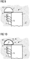
In
Wie auch in den
In
Wie auch in allen anderen Ausführungsbeispielen ist es möglich, dass die Schutzabdeckung
In
Beim Ausführungsbeispiel der
In den bisherigen Figuren ist je nur eine Maßnahme zur Verhinderung von Rückreflektionen in den Resonator der Laserdiode
Speziell bei der Gestaltung der
Durch die Reduzierung oder Eliminierung der optischen Wechselwirkung zwischen der Schutzabdeckung
Im Ausführungsbeispiel der
Durch die facettennah aufgebrauchte Schutzabdeckung
Im Übrigen gelten die Ausführungen zu den
In
Durch das Aufbringen der Antihaftbeschichtung
Das herstellen der Halbleiterbauteile etwa der
Alternativ ist es möglich, die Schutzabdeckung
In
Dazu wird, siehe
Alternativ wird eine Glasperle aufgelegt, gefolgt von einer gezielten lokalen Temperaturbehandlung zur Befestigung analog eines Laserschweißprozesses, auch als Laser Melting Process bezeichnet. Beim Laserschmelzen kann durch eine gezielte Einstellung der Energiedichteverteilung im Strahlprofil, etwa durch ein Gauß-Profil oder ein sogenanntes Top Hat-Profil, die Form des Glastropfens durch lokales Aufschmelzen beeinflusst werden.Alternatively, a glass bead is applied, followed by a targeted local temperature treatment for attachment analogous to a laser welding process, also referred to as Laser Melting Process. In the case of laser melting, the shape of the glass drop can be influenced by local melting by a targeted adjustment of the energy density distribution in the beam profile, for example by a Gaussian profile or a so-called top hat profile.
Beispiele für geeignete Glaszusammensetzungen kommen insbesondere aus der Gruppe der optischen Gläser, speziell Gläser mit einer niedrigen Glasübergangstemperatur von höchstens 400 °C oder Gläser mit einer sehr niedrigen Glasübergangstemperatur von weniger als 300 °C. Solche Gläser basieren bevorzugt auf Glasbildnern wird Telluroxid, Te2O5, Bortrioxid, B2O3, Silica, SiO2, oder Bismutoxid, Bi2O3. Geeignete Glaszusammensetzungen weisen bevorzugt einen hohen Anteil an Netzwerkunterbrechern auf, zum Beispiel ZnO und/oder CaO. Um derartige Glaszusammensetzungen zu stabilisieren oder eine Kristallisationsneigung gering zu halten, kann optional Aluminiumoxid, Al2O3, zugegeben werden.Examples of suitable glass compositions are in particular from the group of optical glasses, especially glasses with a low glass transition temperature of at most 400 ° C. or glasses with a very low glass transition temperature of less than 300 ° C. Such glasses are preferably based on glass formers is tellurium oxide, Te 2 O 5 , boron trioxide, B 2 O 3 , silica, SiO 2 , or bismuth oxide, Bi 2 O 3 . Suitable glass compositions preferably have a high proportion of network breakers, for example ZnO and / or CaO. To stabilize such glass compositions or to minimize crystallization tendency, alumina, Al 2 O 3 , may optionally be added.
Derartige Gläser können auch für das Klebemittel
Alternativ oder zusätzlich erfolgt ein Aufheizen der Laserdiode
Das Prägewerkzeug
Das Heißprägewerkzeug
Die aufgebrachte Schutzabdeckung
Das fertige Halbleiterbauteil
Beim Verfahren der
Nachfolgend, siehe
Beim Ausführungsbeispiel der
Gemäß
Der mindestens eine Leuchtstoff zur Wellenlängenkonversion kann auf eine Region des Leuchtstoffelements
Weiter ist es möglich, dass der Träger
Ebenso ist beim Ausführungsbeispiel der
Solche Leuchtstoffelemente
Auch bei den Gestaltungen der
Die in den Figuren gezeigten Komponenten folgen, sofern nicht anders kenntlich gemacht, bevorzugt in der angegebenen Reihenfolge jeweils unmittelbar aufeinander. Sich in den Figuren nicht berührende Schichten sind bevorzugt voneinander beabstandet. Soweit Linien parallel zueinander gezeichnet sind, sind die entsprechenden Flächen bevorzugt ebenso parallel zueinander ausgerichtet. Ebenfalls, soweit nicht anders kenntlich gemacht, sind die relativen Positionen der gezeichneten Komponenten zueinander in den Figuren korrekt wiedergegeben.Unless otherwise indicated, the components shown in the figures preferably each directly follow one another in the order indicated. Layers not in contact with the figures are preferably spaced apart from one another. As far as lines are drawn parallel to each other, the corresponding surfaces are preferably also aligned parallel to each other. Also, unless otherwise indicated, the relative positions of the drawn components relative to one another are correctly represented in the figures.
Die hier beschriebene Erfindung ist nicht durch die Beschreibung anhand der Ausführungsbeispiele beschränkt. Vielmehr umfasst die Erfindung jedes neue Merkmal sowie jede Kombination von Merkmalen, was insbesondere jede Kombination von Merkmalen in den Patentansprüchen beinhaltet, auch wenn dieses Merkmal oder diese Kombination selbst nicht explizit in den Patentansprüchen oder Ausführungsbeispielen angegeben ist.The invention described here is not limited by the description based on the embodiments. Rather, the invention encompasses any novel feature as well as any combination of features, including in particular any combination of features in the claims, even if this feature or combination itself is not explicitly stated in the patent claims or exemplary embodiments.
BezugszeichenlisteLIST OF REFERENCE NUMBERS
- 11
- Halbleiterlaser und optoelektronisches HalbleiterbauteilSemiconductor laser and optoelectronic semiconductor device
- 22
- Trägercarrier
- 2020
- TrägerseitenflächeCarrier face
- 33
- Laserdiode und optoelektronischer HalbleiterchipLaser diode and optoelectronic semiconductor chip
- 3030
- Facettefacet
- 3131
- StrahlungsaustrittsbereichRadiation exit area
- 3333
- aktive Zoneactive zone
- 44
- Schutzabdeckung/LinseProtective cover / lens
- 4141
- LichteintrittsseiteLight entering side
- 4242
- LichtaustrittsseiteLight output side
- 4343
- Aufrauungroughening
- 4444
- AntireflexbeschichtungAntireflection coating
- 4545
- fotokatalytische Beschichtungphotocatalytic coating
- 4646
- AntihaftbeschichtungNon-stick coating
- 4747
- BrechungsindexanpassungsschichtRefractive index matching layer
- 4848
- Linsenrohmateriallens raw material
- 4949
- HeißprägewerkzeugHot embossing tools
- 55
- Klebemitteladhesive
- 66
- Kavitätcavity
- 6565
- Seitenwand der KavitätSidewall of the cavity
- 77
- LeuchtstoffelementFluorescent element
- 7272
- Eintrittsseiteentry page
- 7373
- dichroitische Beschichtungdichroic coating
- 1010
- Anordnungarrangement
- 1111
- Wärmesenkeheat sink
- 1212
- Umgebungsluftambient air
- 1313
- Bonddrahtbonding wire
- 1414
- Verbindungsmittelconnecting means
- LL
- Laserstrahlunglaser radiation
- RR
- an der Linse reflektierte LaserstrahlungLaser radiation reflected at the lens
- □□
- Winkel zwischen der Facette und der LichteintrittsseiteAngle between the facet and the light entry side
Claims (19)
Priority Applications (10)
| Application Number | Priority Date | Filing Date | Title |
|---|---|---|---|
| DE102017123798.4A DE102017123798B4 (en) | 2017-10-12 | 2017-10-12 | Semiconductor lasers and manufacturing processes for optoelectronic semiconductor components |
| CN201880066473.8A CN111542976A (en) | 2017-10-12 | 2018-10-08 | Semiconductor laser and method for producing an optoelectronic semiconductor component |
| JP2020519069A JP7008808B2 (en) | 2017-10-12 | 2018-10-08 | Manufacturing methods for semiconductor lasers and optoelectronic semiconductor components |
| PCT/EP2018/077313 WO2019072759A1 (en) | 2017-10-12 | 2018-10-08 | Semiconductor laser and method of production for optoelectronic semiconductor parts |
| US16/754,723 US11735887B2 (en) | 2017-10-12 | 2018-10-08 | Semiconductor laser and method of production for optoelectronic semiconductor parts |
| KR1020207013145A KR102425947B1 (en) | 2017-10-12 | 2018-10-08 | Method of manufacturing semiconductor laser and optoelectronic semiconductor devices |
| JP2022002276A JP7256302B2 (en) | 2017-10-12 | 2022-01-11 | semiconductor laser |
| US17/971,156 US11870214B2 (en) | 2017-10-12 | 2022-10-21 | Semiconductor laser and method of production for optoelectronic semiconductor parts |
| JP2023055382A JP2023085409A (en) | 2017-10-12 | 2023-03-30 | semiconductor laser |
| US18/515,928 US20240088622A1 (en) | 2017-10-12 | 2023-11-21 | Semiconductor laser and method of production for optoelectronic semiconductor parts |
Applications Claiming Priority (1)
| Application Number | Priority Date | Filing Date | Title |
|---|---|---|---|
| DE102017123798.4A DE102017123798B4 (en) | 2017-10-12 | 2017-10-12 | Semiconductor lasers and manufacturing processes for optoelectronic semiconductor components |
Publications (2)
| Publication Number | Publication Date |
|---|---|
| DE102017123798A1 true DE102017123798A1 (en) | 2019-04-18 |
| DE102017123798B4 DE102017123798B4 (en) | 2022-03-03 |
Family
ID=63832414
Family Applications (1)
| Application Number | Title | Priority Date | Filing Date |
|---|---|---|---|
| DE102017123798.4A Active DE102017123798B4 (en) | 2017-10-12 | 2017-10-12 | Semiconductor lasers and manufacturing processes for optoelectronic semiconductor components |
Country Status (6)
| Country | Link |
|---|---|
| US (3) | US11735887B2 (en) |
| JP (3) | JP7008808B2 (en) |
| KR (1) | KR102425947B1 (en) |
| CN (1) | CN111542976A (en) |
| DE (1) | DE102017123798B4 (en) |
| WO (1) | WO2019072759A1 (en) |
Cited By (3)
| Publication number | Priority date | Publication date | Assignee | Title |
|---|---|---|---|---|
| DE102018113711A1 (en) | 2018-06-08 | 2019-12-12 | Osram Opto Semiconductors Gmbh | APPARATUS AND HEADLIGHTS |
| DE102020118159A1 (en) | 2020-07-09 | 2022-01-13 | OSRAM Opto Semiconductors Gesellschaft mit beschränkter Haftung | LASER DEVICE |
| DE102022103260A1 (en) | 2022-02-11 | 2023-08-17 | Ams-Osram International Gmbh | LASER COMPONENT |
Families Citing this family (4)
| Publication number | Priority date | Publication date | Assignee | Title |
|---|---|---|---|---|
| DE102018117518A1 (en) | 2018-07-19 | 2020-01-23 | Osram Opto Semiconductors Gmbh | Semiconductor laser |
| KR102344931B1 (en) * | 2020-08-14 | 2021-12-31 | 주식회사 레신저스 | Polymer rod for shaping emitting light to synmetrical light |
| DE102020127450A1 (en) * | 2020-10-19 | 2022-04-21 | OSRAM Opto Semiconductors Gesellschaft mit beschränkter Haftung | OPTOELECTRONIC DEVICE AND METHOD FOR MANUFACTURING OPTOELECTRONIC DEVICE |
| WO2024074254A1 (en) | 2022-10-05 | 2024-04-11 | Ams-Osram International Gmbh | Optoelectronic light source and data glasses |
Citations (5)
| Publication number | Priority date | Publication date | Assignee | Title |
|---|---|---|---|---|
| US5757830A (en) * | 1996-02-07 | 1998-05-26 | Massachusetts Institute Of Technology | Compact micro-optical edge-emitting semiconductor laser assembly |
| US20030007257A1 (en) * | 2001-07-06 | 2003-01-09 | Bell Bernard W. | Facial contact lens system for laser diode |
| DE102004014355A1 (en) * | 2004-03-24 | 2005-10-20 | G L I Global Light Ind Gmbh | Production method for an opto-electronic component like a luminous diode creates a component by reshaping a component's main body through prototyping |
| DE102009040834A1 (en) * | 2009-09-09 | 2011-05-19 | Jenoptik Laserdiode Gmbh | Diode laser component, has sealing device provided for sealing free space with respect to surrounding, and sealing ring sections accomplishing sealing of partial contributions between optics unit and contact bodies, respectively |
| US20130001627A1 (en) * | 2010-04-19 | 2013-01-03 | Harison Toshiba Lighting Corp. | Light emitting device |
Family Cites Families (87)
| Publication number | Priority date | Publication date | Assignee | Title |
|---|---|---|---|---|
| US4001719A (en) * | 1975-08-13 | 1977-01-04 | Bell Telephone Laboratories, Incorporated | Fabrication of a self-aligned mirror on a solid-state laser for controlling filamentation |
| JPS5923479B2 (en) * | 1978-06-22 | 1984-06-02 | 三菱電機株式会社 | Method for manufacturing semiconductor light emitting device |
| JPH0744313B2 (en) * | 1989-02-24 | 1995-05-15 | 日本電信電話株式会社 | Semiconductor laser device |
| JPH02262389A (en) * | 1989-03-31 | 1990-10-25 | Toshiba Corp | Semiconductor laser device and its manufacture |
| JPH0334387A (en) * | 1989-06-29 | 1991-02-14 | Nec Corp | Semiconductor laser device |
| JPH043989A (en) * | 1990-04-20 | 1992-01-08 | Omron Corp | Light-emitting device |
| US5226052A (en) * | 1990-05-08 | 1993-07-06 | Rohm, Ltd. | Laser diode system for cutting off the environment from the laser diode |
| WO1992006521A1 (en) * | 1990-10-01 | 1992-04-16 | United States Department Of Energy | Laser diode assembly including a cylindrical lens |
| US5081639A (en) * | 1990-10-01 | 1992-01-14 | The United States Of America As Represented By The United States Department Of Energy | Laser diode assembly including a cylindrical lens |
| US5206878A (en) * | 1991-10-11 | 1993-04-27 | At&T Bell Laboratories | Wide strip diode laser employing a lens |
| JPH05134150A (en) | 1991-11-11 | 1993-05-28 | Fujitsu Ltd | Manufacture of condenser lens for emission element |
| JP3197034B2 (en) * | 1991-12-04 | 2001-08-13 | シャープ株式会社 | Semiconductor laser device |
| US5274732A (en) * | 1992-01-06 | 1993-12-28 | Eastman Kodak Company | Mount for linear lens array |
| EP0562754A1 (en) * | 1992-03-26 | 1993-09-29 | Hewlett-Packard Company | Optical system for laser devices |
| US5465265A (en) * | 1992-06-24 | 1995-11-07 | Fuji Xerox Co., Ltd. | Multi-beam laser light source and multi-beam semiconductor laser array |
| JP3381073B2 (en) * | 1992-09-28 | 2003-02-24 | ソニー株式会社 | Semiconductor laser device and method of manufacturing the same |
| US5414293A (en) * | 1992-10-14 | 1995-05-09 | International Business Machines Corporation | Encapsulated light emitting diodes |
| ATE156275T1 (en) * | 1993-01-04 | 1997-08-15 | Philips Electronics Nv | BEAM-FORMING OPTICAL ELEMENT, RADIATION SOURCE AND SCANNING UNIT WITH THIS ELEMENT |
| JPH07115244A (en) * | 1993-10-19 | 1995-05-02 | Toyota Motor Corp | Semiconductor laser and its fabrication |
| US5420722A (en) * | 1993-10-25 | 1995-05-30 | Creo Products Inc. | Self-registering microlens for laser diodes |
| US5544184A (en) * | 1994-06-10 | 1996-08-06 | Sdl, Inc. | Semiconductor illumination system with expansion matched components |
| JPH08191172A (en) * | 1995-01-12 | 1996-07-23 | Ricoh Opt Ind Co Ltd | Light-emitting element having minute optical element and minute optical element |
| US5636059A (en) * | 1995-02-08 | 1997-06-03 | Blue Sky Research, Incorporated | Cylindrical microlens external cavity for laser diode frequency control |
| DE19640423C1 (en) | 1996-09-30 | 1998-03-26 | Siemens Ag | Optoelectronic module for bidirectional optical data transmission |
| DE19706276B4 (en) * | 1997-02-18 | 2011-01-13 | Siemens Ag | A semiconductor laser device and method of manufacturing a semiconductor laser device |
| KR100413791B1 (en) * | 1997-05-30 | 2004-02-14 | 삼성전자주식회사 | Blue semiconductor laser device having curve reflector |
| US6636538B1 (en) * | 1999-03-29 | 2003-10-21 | Cutting Edge Optronics, Inc. | Laser diode packaging |
| DE19963805B4 (en) | 1999-12-30 | 2005-01-27 | Osram Opto Semiconductors Gmbh | White light source based on non-linear optical processes |
| JP2001242357A (en) * | 2000-02-28 | 2001-09-07 | Alps Electric Co Ltd | Optical semiconductor device |
| DE10042904C2 (en) * | 2000-08-31 | 2003-03-13 | Infineon Technologies Ag | Semiconductor laser chip with integrated beam former and method for producing a semiconductor laser chip with integrated beam former |
| JP2003059087A (en) | 2001-08-15 | 2003-02-28 | Sony Corp | Optical element, semiconductor laser, optical detector, optical head and optical disk player |
| JP3975066B2 (en) * | 2001-10-12 | 2007-09-12 | 株式会社トプコン | Laser oscillator |
| JP2003207601A (en) | 2002-01-15 | 2003-07-25 | Ricoh Co Ltd | Objective lens, optical pickup module and optical disk device |
| AU2003211414A1 (en) | 2002-03-08 | 2003-09-22 | Sharp Kabushiki Kaisha | Light source apparatus and optical communication module comprising it |
| US20030219211A1 (en) * | 2002-05-22 | 2003-11-27 | Yu-Sik Kim | Method for aligning optical axis of an optical module |
| JP2004072004A (en) * | 2002-08-09 | 2004-03-04 | Keiji Tanaka | Light emitting element having micro-lens, and forming method thereof |
| US7146106B2 (en) * | 2002-08-23 | 2006-12-05 | Amkor Technology, Inc. | Optic semiconductor module and manufacturing method |
| JP4146196B2 (en) * | 2002-09-09 | 2008-09-03 | 株式会社リコー | Composite optical device and manufacturing method thereof |
| US7192199B2 (en) * | 2003-12-26 | 2007-03-20 | Kabushiki Kaisha Toshiba | Optical semiconductor module and method of manufacturing the same |
| WO2005088787A1 (en) * | 2004-03-10 | 2005-09-22 | Matsushita Electric Industrial Co., Ltd. | Coherent light source and optical system |
| CA2502266A1 (en) * | 2004-03-26 | 2005-09-26 | Kyocera Corporation | External resonator and semiconductor laser module using the same |
| US7419839B2 (en) * | 2004-11-12 | 2008-09-02 | Philips Lumileds Lighting Company, Llc | Bonding an optical element to a light emitting device |
| US7444046B2 (en) * | 2005-10-18 | 2008-10-28 | Nlight Photonics Corporation | Diode laser array coupling optic and system |
| JP4961733B2 (en) | 2005-12-05 | 2012-06-27 | ソニー株式会社 | Semiconductor laser device manufacturing method and semiconductor laser device |
| JP2008146750A (en) | 2006-12-11 | 2008-06-26 | Matsushita Electric Ind Co Ltd | Optical member sticking method for semiconductor device |
| US7764722B2 (en) * | 2007-02-26 | 2010-07-27 | Nichia Corporation | Nitride semiconductor laser element |
| JP2009088066A (en) * | 2007-09-28 | 2009-04-23 | Panasonic Corp | Semiconductor apparatus |
| WO2009041462A1 (en) * | 2007-09-28 | 2009-04-02 | Sanyo Electric Co., Ltd. | Nitride-group semiconductor light-emitting element, nitride-group semiconductor laser element, nitride-group semiconductor light emitting diode, their manufacturing method, and nitride-group semiconductor layer forming method |
| JP5228434B2 (en) * | 2007-10-15 | 2013-07-03 | 日亜化学工業株式会社 | Light emitting device |
| DE102007063438A1 (en) * | 2007-12-21 | 2009-06-25 | Eagleyard Photonics Gmbh | Laser module, has cylindrical lens mounted on heat sink in front of laser such that radiation field of high-power laser diode does not cross heat sink, and laser chip fastened downwards on sub carrier with active zone |
| JP2009251224A (en) * | 2008-04-04 | 2009-10-29 | Sumitomo Electric Ind Ltd | Optical module and method for assembling the same |
| JP2009260118A (en) * | 2008-04-18 | 2009-11-05 | Konica Minolta Opto Inc | Optical module |
| WO2010011392A2 (en) * | 2008-05-08 | 2010-01-28 | Massachusetts Institute Of Technology (Mit) | Lens coupled quantum cascade laser |
| JP5443356B2 (en) | 2008-07-10 | 2014-03-19 | 株式会社東芝 | Semiconductor laser device |
| JP4982469B2 (en) * | 2008-10-31 | 2012-07-25 | 株式会社日立製作所 | Optical module |
| JP2010147359A (en) * | 2008-12-22 | 2010-07-01 | Hitachi Ltd | Optical module |
| JP2011003889A (en) * | 2009-05-21 | 2011-01-06 | Nichia Corp | Semiconductor laser device and method for manufacturing the same |
| JP5707862B2 (en) | 2009-11-05 | 2015-04-30 | 日亜化学工業株式会社 | Semiconductor laser device and manufacturing method thereof |
| US8743917B2 (en) * | 2009-12-14 | 2014-06-03 | Panasonic Corporation | Wavelength conversion light source, optical element and image display device |
| DE102010015197A1 (en) * | 2010-04-16 | 2012-01-19 | Osram Opto Semiconductors Gmbh | Laser light source |
| JP2012212734A (en) | 2011-03-30 | 2012-11-01 | Nichia Chem Ind Ltd | Semiconductor laser device |
| JP5996215B2 (en) * | 2012-02-28 | 2016-09-21 | オリンパス株式会社 | Photoelectric conversion module and optical transmission unit |
| CN102872779B (en) | 2012-07-27 | 2014-12-17 | 深圳大学 | Method for preparing photonic crystal fiber for light-catalyzed reaction |
| DE102012106943B4 (en) * | 2012-07-30 | 2019-06-27 | Osram Opto Semiconductors Gmbh | Method for producing a semiconductor laser diode and semiconductor laser diode |
| KR20140021483A (en) | 2012-08-09 | 2014-02-20 | 한국전자통신연구원 | Optical transmitter and optical transceiver comprising optical transmitter |
| US20140044436A1 (en) | 2012-08-09 | 2014-02-13 | Electronics And Telecommunications Research Institute | Optical transmitter and optical transceiver comprising optical transmitter |
| DE102012215684A1 (en) * | 2012-09-04 | 2014-03-06 | Osram Opto Semiconductors Gmbh | Method for manufacturing laser component i.e. laser package, for surface mounting technology assembly, involves positioning laser chip on supporting substrate, where side surface of laser chip is attached with stop element |
| DE102012217652B4 (en) * | 2012-09-27 | 2021-01-21 | OSRAM Opto Semiconductors Gesellschaft mit beschränkter Haftung | Optoelectronic component |
| JP5616471B2 (en) * | 2013-03-05 | 2014-10-29 | 株式会社フジクラ | Semiconductor laser module and manufacturing method thereof |
| EP2720326A1 (en) | 2013-03-12 | 2014-04-16 | Axetris AG | Gas detection laser light source with reduced optical feedback |
| DE102013205594A1 (en) * | 2013-03-28 | 2014-10-02 | Osram Opto Semiconductors Gmbh | Laser component and method for its production |
| JP2014232790A (en) * | 2013-05-29 | 2014-12-11 | パナソニック株式会社 | Semiconductor laser device and manufacturing method thereof |
| WO2014192939A1 (en) * | 2013-05-30 | 2014-12-04 | 古河電気工業株式会社 | Optical module |
| US11646549B2 (en) * | 2014-08-27 | 2023-05-09 | Nuburu, Inc. | Multi kW class blue laser system |
| JP6843745B2 (en) * | 2014-10-14 | 2021-03-17 | ヘプタゴン・マイクロ・オプティクス・プライベート・リミテッドHeptagon Micro Optics Pte. Ltd. | Optical element stack assembly |
| JP6508466B2 (en) * | 2015-05-29 | 2019-05-08 | セイコーエプソン株式会社 | Light source device and projector |
| US10033151B2 (en) * | 2015-12-15 | 2018-07-24 | Nlight, Inc. | Laser module with meniscus collimating lens |
| JP7024410B2 (en) * | 2016-01-28 | 2022-02-24 | ソニーグループ株式会社 | Semiconductor light emitting device |
| DE102016101942B4 (en) * | 2016-02-04 | 2022-07-21 | OSRAM Opto Semiconductors Gesellschaft mit beschränkter Haftung | Method for producing an optoelectronic lighting device |
| US10048498B2 (en) * | 2016-03-25 | 2018-08-14 | Microsoft Technology Licensing, Llc | Illumination module |
| US10551596B2 (en) * | 2016-06-29 | 2020-02-04 | Ams Sensors Singapore Pte. Ltd. | Optical and optoelectronic assemblies including micro-spacers, and methods of manufacturing the same |
| EP3602703A1 (en) * | 2017-04-07 | 2020-02-05 | Huawei Technologies Co., Ltd. | Laser |
| US10404038B2 (en) * | 2017-06-22 | 2019-09-03 | Sumitomo Electric Industries, Ltd. | Quantum cascade laser |
| DE102018106959A1 (en) * | 2018-03-23 | 2019-09-26 | Osram Opto Semiconductors Gmbh | OPTOELECTRONIC COMPONENT AND METHOD FOR PRODUCING AN OPTOELECTRONIC COMPONENT |
| CN108400520B (en) * | 2018-03-28 | 2024-04-09 | 赵智亮 | Wavelength Continuously Tunable Single Longitudinal Mode Semiconductor Laser |
| DE102018117518A1 (en) * | 2018-07-19 | 2020-01-23 | Osram Opto Semiconductors Gmbh | Semiconductor laser |
| DE102018128751A1 (en) * | 2018-11-15 | 2020-05-20 | Osram Opto Semiconductors Gmbh | Semiconductor laser |
-
2017
- 2017-10-12 DE DE102017123798.4A patent/DE102017123798B4/en active Active
-
2018
- 2018-10-08 WO PCT/EP2018/077313 patent/WO2019072759A1/en active Application Filing
- 2018-10-08 US US16/754,723 patent/US11735887B2/en active Active
- 2018-10-08 CN CN201880066473.8A patent/CN111542976A/en active Pending
- 2018-10-08 KR KR1020207013145A patent/KR102425947B1/en active IP Right Grant
- 2018-10-08 JP JP2020519069A patent/JP7008808B2/en active Active
-
2022
- 2022-01-11 JP JP2022002276A patent/JP7256302B2/en active Active
- 2022-10-21 US US17/971,156 patent/US11870214B2/en active Active
-
2023
- 2023-03-30 JP JP2023055382A patent/JP2023085409A/en active Pending
- 2023-11-21 US US18/515,928 patent/US20240088622A1/en active Pending
Patent Citations (5)
| Publication number | Priority date | Publication date | Assignee | Title |
|---|---|---|---|---|
| US5757830A (en) * | 1996-02-07 | 1998-05-26 | Massachusetts Institute Of Technology | Compact micro-optical edge-emitting semiconductor laser assembly |
| US20030007257A1 (en) * | 2001-07-06 | 2003-01-09 | Bell Bernard W. | Facial contact lens system for laser diode |
| DE102004014355A1 (en) * | 2004-03-24 | 2005-10-20 | G L I Global Light Ind Gmbh | Production method for an opto-electronic component like a luminous diode creates a component by reshaping a component's main body through prototyping |
| DE102009040834A1 (en) * | 2009-09-09 | 2011-05-19 | Jenoptik Laserdiode Gmbh | Diode laser component, has sealing device provided for sealing free space with respect to surrounding, and sealing ring sections accomplishing sealing of partial contributions between optics unit and contact bodies, respectively |
| US20130001627A1 (en) * | 2010-04-19 | 2013-01-03 | Harison Toshiba Lighting Corp. | Light emitting device |
Cited By (5)
| Publication number | Priority date | Publication date | Assignee | Title |
|---|---|---|---|---|
| DE102018113711A1 (en) | 2018-06-08 | 2019-12-12 | Osram Opto Semiconductors Gmbh | APPARATUS AND HEADLIGHTS |
| WO2019234180A1 (en) | 2018-06-08 | 2019-12-12 | Osram Opto Semiconductors Gmbh | Apparatus and headlight |
| US11603031B2 (en) | 2018-06-08 | 2023-03-14 | Osram Oled Gmbh | Apparatus and headlight |
| DE102020118159A1 (en) | 2020-07-09 | 2022-01-13 | OSRAM Opto Semiconductors Gesellschaft mit beschränkter Haftung | LASER DEVICE |
| DE102022103260A1 (en) | 2022-02-11 | 2023-08-17 | Ams-Osram International Gmbh | LASER COMPONENT |
Also Published As
| Publication number | Publication date |
|---|---|
| US20200313399A1 (en) | 2020-10-01 |
| JP7256302B2 (en) | 2023-04-11 |
| WO2019072759A1 (en) | 2019-04-18 |
| KR20200103629A (en) | 2020-09-02 |
| US11735887B2 (en) | 2023-08-22 |
| JP2023085409A (en) | 2023-06-20 |
| JP2022058552A (en) | 2022-04-12 |
| JP2020537337A (en) | 2020-12-17 |
| CN111542976A (en) | 2020-08-14 |
| US20230068945A1 (en) | 2023-03-02 |
| US11870214B2 (en) | 2024-01-09 |
| DE102017123798B4 (en) | 2022-03-03 |
| JP7008808B2 (en) | 2022-01-25 |
| US20240088622A1 (en) | 2024-03-14 |
| KR102425947B1 (en) | 2022-07-27 |
Similar Documents
| Publication | Publication Date | Title |
|---|---|---|
| DE102017123798B4 (en) | Semiconductor lasers and manufacturing processes for optoelectronic semiconductor components | |
| DE112015005762B4 (en) | Light-emitting device and method for making the same | |
| EP1792351B1 (en) | Housing for an optoelectronic component, optoelectronic component and method for the production of an optoelectronic component | |
| WO2011104364A1 (en) | Radiation-emitting component comprising a semiconductor chip and a conversion element and method for producing it | |
| EP2596534B1 (en) | Radiation-emitting component and method for producing radiation-emitting components | |
| EP3084848B1 (en) | Conversion element, method for the production of a conversion element, optoelectronic component comprising a conversion element | |
| DE112014005897B4 (en) | Conversion element, component and method for producing a component | |
| WO2006089540A2 (en) | Method for producing an optical, radiation-emitting component and optical, radiation-emitting component | |
| WO2008131736A1 (en) | Optoelectronic component and method for producing a plurality of optoelectronic components | |
| WO2019179769A1 (en) | Optoelectronic component and method for producing an optoelectronic component | |
| DE102015116336B4 (en) | Semiconductor laser | |
| WO2012084451A1 (en) | Optoelectronic semiconductor component | |
| DE102013207308B4 (en) | Method for manufacturing an optoelectronic assembly and optoelectronic assembly | |
| EP2652806A1 (en) | Method for generating a luminescence conversion material layer, composition therefor and component comprising such a luminescence conversion material layer | |
| DE102013112549A1 (en) | Process for the production of optoelectronic semiconductor components and optoelectronic semiconductor component | |
| DE102007046348A1 (en) | Radiation-emitting device with glass cover and method for its production | |
| DE102016104616B4 (en) | Semiconductor light source | |
| DE102008012407A1 (en) | Radiation-emitting device | |
| DE102014117983A1 (en) | Conversion element, optoelectronic semiconductor component and method for producing conversion elements | |
| DE102016111442A1 (en) | Semiconductor light source | |
| DE112017001296B4 (en) | semiconductor light source | |
| DE102011113963A1 (en) | Optoelectronic semiconductor component e.g. LED, for generating e.g. electromagnetic infrared radiation, has conversion element performing conversion of primary radiation into secondary radiation from spectral region of infrared radiation | |
| DE102016121099A1 (en) | PREPARATION OF RADIATION-EMITTING SEMICONDUCTOR COMPONENTS | |
| WO2013041465A1 (en) | Wavelength conversion element and light-emitting semiconductor component comprising wavelength conversion element | |
| EP2586069B1 (en) | Method for producing a semiconductor component |
Legal Events
| Date | Code | Title | Description |
|---|---|---|---|
| R163 | Identified publications notified | ||
| R012 | Request for examination validly filed | ||
| R016 | Response to examination communication | ||
| R018 | Grant decision by examination section/examining division | ||
| R130 | Divisional application to |
Ref document number: 102017012409 Country of ref document: DE |
|
| R020 | Patent grant now final |